國 立 交 通 大 學
電子工程學系電子研究所
碩 士 論 文
應用於視訊系統之快速相位追蹤與高頻
率倍數全數位式鎖相迴路
A Fast Phase-Tracking ADPLL for Video
Applications with Large Frequency
Multiplication Factor
研究生 : 張琇茹
指導教授 : 李鎮宜博士
應用於視訊系統之快速相位追蹤與高頻率倍數
全數位式鎖相迴路
A Fast Phase-Tracking ADPLL for Video
Applications with Large Frequency
Multiplication Factor
研 究 生:張琇茹
Student:Shiou-Ru Jang
指導教授:李鎮宜 教授
Advisor:Prof. Chen-Yi Lee
國 立 交 通 大 學
電機學院 電子工程所碩士班
碩 士 論 文
A Thesis
Submitted to Institute of Electronics College of Electrical and Computer Engineering
National Chiao Tung University in Partial Fulfillment of the Requirements
for the Degree of Master
in
Electronics Engineering Aug. 2008
Hsinchu, Taiwan, Republic of China
應用於視訊系統之快速相位追蹤與高頻率
倍數全數位式鎖相迴路
研究生: 張琇茹 指導教授: 李鎮宜 國立交通大學 電子工程學系 電子研究所碩士班摘 要
在本論文中,我們提出一個快速相位追蹤的高頻率倍數全數位式鎖相迴路, 此電路可應用於視訊系統中的時脈產生器,其主要功能是接收顯示卡發出的水平 同步訊號,依據使用者設定的螢幕解析度,產生高頻像素時脈來擷取類比的視訊 訊號資料。取樣點和資料的相位差直接影響到顯示畫面的品質,若是像素時脈的 相位不穩定,則顯示畫面會閃爍或抖動。因此,如何在高頻率倍數下,及時的追 蹤與補償相位誤差,是此電路設計的重點。 在提出的架構中,我們使用了三角積分調變器來改進數位控制震盪器的等效 解析度,並且加入時間數位轉換器迴路來即時補償相位誤差,另外針對數位控制 震盪器中可能發生的不預期的突波作分析和預防。我們使用標準元件庫來設計整 個晶片,並利用合成軟體及自動佈局工具實現電路,最後以 0.18 微米 1P5M 標準 CMOS 製程來製作晶片。A Fast Phase-Tracking ADPLL for Video
Applications with Large Frequency
Multiplication Factor
Student: Shiou-Ru Jang Advisor: Chen-Yi Lee Department of Electronics Engineering and Institute of Electronics,
National Chiao-Tung University
Abstract
In this thesis, a fast phase-tracking all-digital phase-locked loop with large multiplication factor is presented. This circuit can be applied to the video system as a clock generator. It receives the horizontal synchronous signal from the graphics card and then generates a high frequency pixel clock according to the monitor resolution setting to acquire the video signal data. The phase error between sampling clock and video data affects the display image quality directly. If the phase of pixel clock is not stable, the display image will be glittering or jittering. Therefore, how to design a fast phase-tracking clock generator with large multiplication factor is the point of this thesis.
In the proposed architecture, a sigma-delta modulator is used to enhance the equivalent digital-controlled oscillator resolution, and a time-to-digital converter loop is applied to compensate the phase error immediately, and the glitch of DCO is also analyzed and prevented. This chip is implemented with standard cell library by synthesis and auto place-and-route tools, and realized using 0.18μm 1P5M standard CMOS process.
致謝
在SI2 實驗室的這兩年,是我有生以來最密集的吸收知識的時光。非常感謝 我的指導老師李鎮宜教授提供超完善的研究設備和環境,老師的諄諄教誨和明確 的方向感總是給我很大的啟發。並且在老師帶領下的實驗室相當和樂融融,使我 在研究的路上毫不孤單。感謝超厲害的鍾菁哲學長超有耐心不厭其煩的在我研究 的路上指引方向,每週的討論經常使我對電路的概念茅塞頓開豁然開朗,在學長 身上除了學到非常非常多的專業知識,也學習到許多解決問題的方法。感謝所有 鼓勵我和指引我的人使我能順利的完成碩士論文。最後感謝我的家人總是支持我 任何的決定,給我無限的信任。Contents
Chapter 1 Introduction ...1
1.1 Video Display System Overview ...1
1.2 Motivation...4
1.3 Thesis Organization ...5
Chapter 2 Design overview...6
2.1 Paper Survey ...6
2.1.1 A Fractural-DLL Based Clock Generator for Video Application...6
2.1.2 Video Capture PLL by Analog bits inc. ...7
2.1.3 Summary...8
2.2 Design Challenge...8
2.2.1 The Difficulty of Large Multiplication Factor ADPLL Design ...9
2.2.2 The Impact of HSYNC Jitter Injection ...10
2.2.3 Digital Controlled Oscillator glitch ...11
Chapter 3 Architecture of fast Phase-tracking ADPLL...14
3.1 Phase/Frequency Detector ...15
3.1.1 Structure...15
3.1.2 Simulation Result...16
3.2 Digital Controlled Oscillator...17
3.2.1 Structure...17
3.2.2 Solutions of Digital Controlled Oscillator Glitch ...18
3.2.3 Problem of Uniform Resolution...19
3.2.4 Simulation result ...20
3.3 Control Logic...24
3.3.1 State diagram ...24
3.3.2 Digital Loop Filter ...27
3.4 Dithering Technique...29
3.4.1 Dithering Theorem...29
3.4.2 Sigma Delta Modulator Overview ...31
3.4.3 Sigma Delta Modulator Structure and Working Principle ...33
3.4.4 Simulation Result...34
3.5 Time-to-Digital Converter Loop...35
3.5.1 Working Principle ...36
3.5.2 Structure...37
Chapter 4 Chip Implementation...46
4.1 Chip Layout View ...46
4.2 Overall Simulation...49
4.2.1 Simulations in Verilog...49
4.2.2 Simulations in AMS...51
4.2.3 Post-layout Simulation...52
Chapter 5 Conclusion and Future Work...54
Figure List
Fig. 1.1 Video display system ...1
Fig. 1.2 Video analog signal vs. sampling clock diagram...3
Fig. 1.3 Relationship between V/Hsync and pixel clock ...3
Fig. 2.1 Fractural-DLL based clock generator [5] ...6
Fig. 2.2 Video Capture PLL [3] ...7
Fig. 2.3 Jitter versus multiplication factor at fixed 240-MHz output [8]...8
Fig. 2.4 The tracking jitter design challenge of large multiplication factor...9
Fig. 2.5 The weakness of phase-tracking in ADPLL with Bang-bang PFD ...11
Fig. 2.6 Glitch in path selector...11
Fig. 2.8 Details of target-type glitch ...12
Fig. 2.9 Details of original-type glitch...13
Fig. 3.1 The block diagram of proposed ADPLL, and the main targets of each block14 Fig. 3.2 The modified 3-state PFD architecture [9] ...15
Fig. 3.3 Pulse amplifier structure [9] ...16
Fig. 3.4 Simulation result of PFD circuit...16
Fig. 3.5 A cell-based MUX type DCO structure...17
Fig. 3.6 Fine-tuning stage of DCO...18
Fig. 3.7 Modified DCO structure...19
Fig. 3.8 The difficult of uniform resolution in DCO code changing over stage...20
Fig. 3.9 Simulation of DCO period versus coarse code 0 ~ 127 ...21
Fig. 3.10 Comparison of DCO period in PVT variation...22
Fig. 3.11 Simulation of DCO period of coarse code and fine code ...23
Fig. 3.12 The finite state diagram of PLL controller ...24
Fig. 3.13 Timing diagram in Coarse SAR state ...25
Fig. 3.14 Timing diagram in Frequency Searching state ...26
Fig. 3.15 PLL Frequency and Phase Tracking Procedure...27
Fig. 3.16 Digital Loop Filter Block Diagram ...28
Fig. 3.17 Dithering technique enhances period resolution ...29
Fig. 3.18 Phase error reduction by dithering technique ...30
Fig. 3.19 First-order SDM Structure...31
Fig. 3.20 Modified first-order SDM ...33
Fig. 3.21 The working principle of SDM [11] ...33
Fig. 3.22 Simulation with different fractional code bits ...35
Fig. 3.24 TDC structure [15]...37
Fig. 3.25 Simulation the phase error of PLL with and without TDC in VGA to UXGA ...39
Fig. 3.26 Example of HSYNC jitter models...41
Fig. 3.27 Simulation without TDC ...42
Fig. 3.28 Simulation with different TDC gain and different HSYNC jitter ratio ...43
Fig. 3.29 Phase error vs. HSYNC jitter ratio with different TDC gain ...44
Fig. 3.30 Measurement of the practical HSYNC jitter ...45
Fig. 4.1 Floor plan and I/O plan...46
Fig. 4.2 Layout of proposed ADPLL ...48
Fig. 4.3 Verilog simulation with 6 bits and 8 bits fractional code ...49
Fig. 4.4 Verilog simulation with on/off TDC loop...50
Fig. 4.5 AMS simulation with 8bits fractional code and TDC loop ...52
Table List
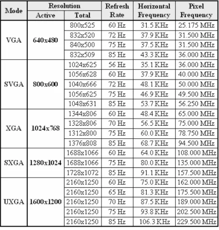
Table 1.1 Monitor timing specification...2
Table 3.1 Summary of peak-to-peak phase drift in different fractional code bits ...35
Table 3.2 Summary of the TDC performance...38
Table 3.3 Phase Error in Different Operation Modes (phase error unit: %) ...39
Table 3.4 Ideal TDC Gain for Different Operation Mode ...41
Chapter 1 Introduction
1.1 Video Display System Overview
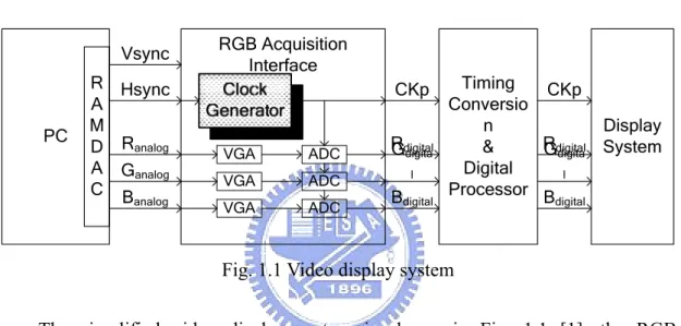
PC R A M D A C Vsync Hsync Ranalog Ganalog Banalog RGB Acquisition Interface VGA VGA VGA ADC ADC ADC Timing Conversio n & Digital Processor Display System RGdigitaldigita l Bdigital CKp CKp RGdigitaldigita l Bdigital
Fig. 1.1 Video display system
The simplified video display system is shown in Fig. 1.1 [1], the RGB (Red/Green/Blue) analog signal, Vertical Synchronous clock (Vsync), and Horizontal Synchronous clock (Hsync) are sent from Random Access Memory Digital-Analog Converter (RAMDAC) of Personal Computer (PC) to the RGB acquisition interface. The RGB signal has been converted to digital domain from Variable Gain Amplifier (VGA), Analog-to-Digital Converter (ADC) in RGB acquisition interface, and the Pixel Clock (CKp) is also generated by it. Then the digital RGB signal can be computed in the following digital processes.
The clock for ADC to sample analog data to digital is generated from a clock generator which is usually composed of a Phase-Lock Loop (PLL), and the high speed pixel clock (CKp) is produced according to the setting of display quality, and is aligned
to the Hsync. The multiplication factor between Hsync and pixel clock is proportion to the display horizontal resolution which is defined according to the display specifications in video electronics standards association (VESA). That means the display resolution has to be improved for the quality of display.
Table 1.1 Monitor timing specification
As shown in the Table 1.1, the multiplication factor of the clock generator in video system applications is very large, for example, 2160 in UXGA. The input frequency is very low, for example, 75kHz Horizontal frequency in UXGA. Besides, the range of pixel frequency is from 25MHz to 229.5MHz which is difficult for designers to realize an oscillator to cover such wide range. The stability of PLL loop is not good in this situation in traditional design, and the output jitter is also not easy to be controlled.
Fig. 1.2 Video analog signal vs. sampling clock diagram
Besides, the high speed pixel clock has to be aligned to Hsync, otherwise an ambiguous signal will be sampled. The relationship between phase of pixel clock and analog RGB signal is shown in Fig. 1.2. The edges of pixel clock have to be located in static signal region, otherwise the converted digital signals would be ambiguous which result in blurry display image.
However, the input of clock generator Hsync comes in with high noise and low frequency pulse. How to improve the loop stability in large multiplication and low input frequency, and align the phase of a highly noisy Hsync clock become the main considerations of video capture clock generator design.
Vsync Vback Vdisplay(N Hsync cycles) Vfront Vsync
Vsync Vback Vdisplay(M pixel clocks) Vfront Vsync
Vsync Hsync Video Data Hsync Pixel Clock Video Data
The relationship between Vsync, Hsync, and Pixel clock is shown in Fig. 1.3. The Hsync clock string is generated by Vsync, and the Pixel clock is generated by Hsync. The video data is sampled by pixel clock and converted to digital domain by ADC. The display resolution directly corresponds to the multiplication factor M and N.
1.2 Motivation
The main targets of the clock generator for video application are tracking the phase of a highly noisy and low frequency HSYNC from the display-card, and generating the high speed pixel clock, with large multiplication factor from 800 to 2160 times [1].
Some analog approaches are proposed to accomplish these targets. For example, an architecture which separates the frequency and phase operation into two loop filters [2] is proposed to help phase tracking and to meet the specification. The second example of PLL for video application employs 3 PLLs, an internal PLL is used to generate a 5-phase 660MHz extra high frequency clock from an additional crystal as a high precision time resolution [3], and then it utilizes a high-precision 28-bit digital frequency synthesizer to generate an output clock. The third example applies a 2-stage cascaded PLL to overcome the low-rate input clock [4]. However, those analog approaches often result in larger power consumption, long lock-in time. Furthermore, because of the small input frequency, the loop filters (LPF) of analog PLL need external RC components.
Some digital approaches are also realized for this application. A DLL-based clock generator with analog variable delay cell and charge pump is proposed to accomplish the specification [5]. Another example of a digital PVT tolerant PLL for large
multiplication frequency synthesizer employs a digital controller, DAC, and VCO [6]. Both the digital controlled clock generator designs utilize the customized analog oscillator for high resolution in frequency to overcome the difficulty of large multiplication design.
From the development of CMOS process, a cell-based all-digital PLL has become more and more popular because of high integration in SOC design, good immunity against switching noise, better portability for technology scaling, and low leakage current in advanced process.
In this thesis, a cell-based all-digital PLL circuit for video application with large multiplication is proposed. The main target is to accommodate to the current monitor timing specifications [7]. This chip is implemented in a 0.18μm 1p5m 1.8v/3.3v standard CMOS process. The chip area is 1000×1000μm2, and the power consumption
is 6.65mW at 6MHz input clock, 192MHz output clock.
1.3 Thesis Organization
This thesis is arranged as follow. In chapter 2, the surveys of video application PLL and the design challenges are described. In chapter 3, all the details of the proposed ADPLL clock generator, including the circuit architecture, functional blocks, control algorithm, and block simulation results are presented. The chip implementation and overall simulation results are reported in chapter 4. Finally, we make conclusions and discuss future work in chapter 5.
Chapter 2 Design overview
2.1 Paper Survey
2.1.1 A Fractural-DLL Based Clock Generator for Video
Application
Fig. 2.1 Fractural-DLL based clock generator [5]
The design of a fractural-DLL based clock generator for video application is shown in Fig. 2.1. A variable delay cell with analog PFD and charge pump is used in
multiplication and noisy input jitter. Amultiple-set and single-reset flip-flop is used to generate pixel clock ckout. However, it needs an initial circuit to generate a pulse
before the flip-flop, and may result in an additional phase drift. The cycle-to-cycle output jitter of this design is 17 ps rms at 210 MHz. The phase error is roughly equal to
1.6ns, which represents less than one third of a pixel length in the standard.
2.1.2 Video Capture PLL by Analog bits inc.
5 Phase Reference PLL Divider2 Hybrid PFD Control Loop Digital 10 Phase 28 bit NCO 10 Phase Interpolartor 8 Phase PLL Delay 12 bit Divider Resynchronize Reference Hsync_in Hsync_out Pixel Phase Fine Phase 660MHz 5 Phase Reference 330MHz Line
Phase is 1/8, Fine Phase is 1/32
Fig. 2.2 Video Capture PLL [3]
The other example of video capture PLL by Analog Bits Inc is illustrated in Fig. 2.2. This PLL circuit is composed of two internal PLLs inside the overall PLL. One internal PLL is used to generate a 5-phase 660MHz clock from a 14.3MHz system reference clock as a high precision time reference. The other internal PLL is used to generate an 8-phase clock. After generating a high precision time reference, a programmable all-digital loop filter and a high precision 28-bit digital frequency synthesizer are utilized to generate an output clock with less jitter. Besides, a 12-bit clock divider with programmable frequency multiplication factor, and a controllable delay line is inserted in the output path for de-skew purpose. This design is the most popular one in video application.
2.1.3 Summary
From the surveys above, high-resolution oscillators are required in clock generator designs with large multiplication. However, an analog voltage controlled oscillator is not portable, and becomes more difficult to design in advanced process.
In order to track the noisy and slow frequency input clock, an internal extra high frequency clock is introduced to overcome the challenge, but it requires more cost and power consumption, for example, 3 PLLs employing. Another solution is to utilize an analog loop filter, but it requires external RC components. In advance process, a leakage current problem will also reduce the performance of whole loop and cause additional power lost.
2.2 Design Challenge
The tracking jitter is strongly related to the multiplication factor as shown in the Fig. 2.3. The period jitter is controlled in 5%, but the tracking jitter exceed 100% when the multiplication factor is larger than 512 which means it is hard to accomplish phase tracking when ADPLL has large multiplication factor.
Secondly, Hsync is not generated by crystal oscillator in video system application, and the jitter might be up to 1ns. The stability of ADPLL loop may be destroyed by the trembling of Hsync.
2.2.1 The Difficulty of Large Multiplication Factor
ADPLL Design
Fig. 2.4 The tracking jitter design challenge of large multiplication factor Because the significant Video ADPLL multiplication factor is up to 800 ~ 2160, the minor frequency error or input jitter will lead to enormous error. As shown in Fig. 2.4, the original assumption that the closest output pixel clock period is T, the DCO resolution is Δ, and the multiplication factor is N. After a HSYNC cycle, the phase of HSOUT is slightly behind the phase of HSYNC for the amount of δ. Then the PLL controller adjusts Pixel clock period to T-Δ. After another HSYNC cycle, HSOUT substantially leads HSYNC, and the phase error becomes δ−N×Δ. Therefore, despite the pixel clock cycle only adjusts for the amount of Δ, the large multiplication factor
still result in considerable phase error. Hence, the improvement of the DCO resolution is necessary.
From this example, even one resolution have been tuned, the phase error is amplified by the high multiplication factor. For this reason, the enhancement of resolution is necessary. Nonetheless, even if the resolution is reduced to 1ps, a single tuning step of HSOUT period reaches 2.16ns after being amplified by the multiplication factor (2160). There are two solutions for this problem: the reduction of the DCO resolution of DCO architecture and the modification of the PLL architecture. However, the DCO reality resolution cannot be reduced unlimited, so we solve this problem by modifying the PLL architecture.
2.2.2 The Impact of HSYNC Jitter Injection
Unlike the conventional analog PLL Charge Pump, the All-Digital PLL with Bang-bang PFD can only get the lead or lag information, and have no phase error “quantity” information. Therefore, in the application of high multiplication factor PLL loop, it is very difficult to track phase.
Moreover, the tuning step of the DCO after lock has to keep small for the amplification of phase error by large multiplication factor. However, a small tuning step slows down the phase tracking behavior and causes a phase drift accumulation by HSYNC jitter.
Fig. 2.5 shows the problem mentioned above. The maximum value of the input HSYNC jitter is 1.2 ns, but the phase drift is accumulated to 6 ns because of the low tracking speed of HSOUT. Therefore the design of noisy input application like Video
Capture PLL must have the ability to keep up with the phase of HSYNC immediately, otherwise the accumulated phase error will be very substantial.
0 5 10 15 20 25 30 35 40 45 50 -8 -6 -4 -2 0 2 4 6 # of period jit te r (n s)
TDCnoM PhaseError(p-p)=+-7.096(ns) gain=0.0 ratio=19.7
HSYNC jitter HSOUT jitter Phase Drift Filter jitter
Fig. 2.5 The weakness of phase-tracking in ADPLL with Bang-bang PFD
2.2.3 Digital Controlled Oscillator glitch
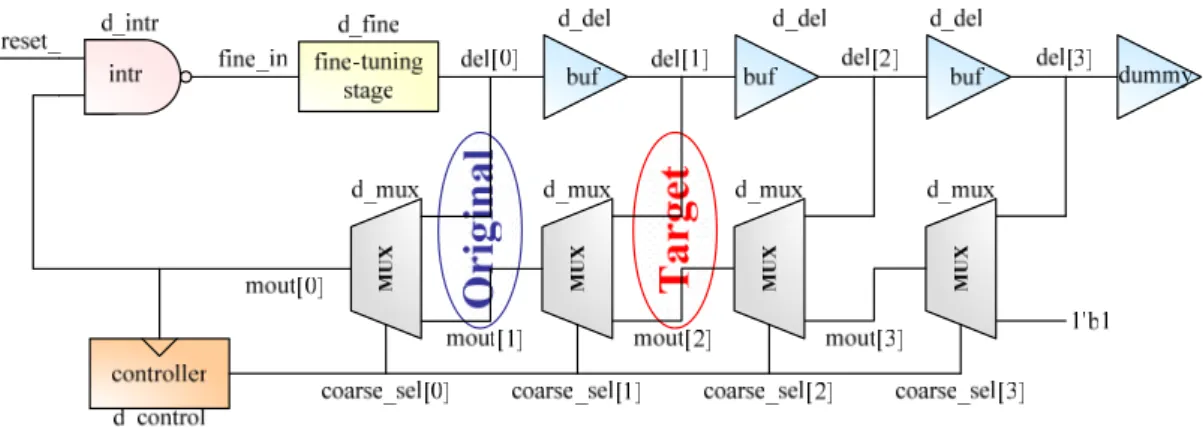
Although the cell-based MUX-type DCO and DCV fine-tuning stage can achieve a high resolution, wide operating range, and high operating frequency. There are still some problems for wide application. The most important problem of path-select-type DCO is the occurrence of glitch. A glitch generates uncertain output signal, and the frequency divider will be disordered.
Fig. 2.6 Glitch in path selector
The change of the path-select-signal when two inputs of multiplexer are inconsistent will cause a glitch as shown in Fig. 2.6. In order to clarify the timing of glitch occurrence, we define the glitch by the location where the glitch take places. Two types of the glitch discussed here are target-type and original-type, as shown in Fig. 2.7.
Fig. 2.7 Definition of glitch
Assume that mout[0] is the output of the DCO. When the coarse_sel[0:3] changes from 1000 to 0100, the target-type jitter occurs at the target path, that is, del[1] and mout[2]. A glitch will be generated when del[1] is different from mout[2], but the mout[2] has already fixed at high, so the code have to be changed when del[1] is high to avoid glitch occurrence.
Fig. 2.8 Details of target-type glitch
As shown in Fig. 2.8, in order to avoid the glitch occurrence, the delay of del[0] Æ mout[0] Æ coarse_sel has to be larger than the delay of del[0] Æ del[1]. The inference of timing limitation equation is shown below.
d_mux+d_control>d_del (posedge del[0] is origin) Lower limit: d_control>d_del-d_mux
(if d_mux is larger than d_del, d_control can be zero) →
From the equation above, the lower limitation of d_control is negative if the d_mux is larger than d_del, that is, the target-type glitch will not occur when d_mux is larger than d_del.
The other type of glitch occurs at original path, del[0] and mout[1], is called original-type glitch, as shown in Fig. 2.9. A glitch occurs when del[0] is different from mout[1], and mout[1] has fix at high when coarse_sel[0] is 1.
Fig. 2.9 Details of original-type glitch
The delay of del[0] to coarse_sel[0] must be smaller than that of del[0]Æ mout[0]Æfine_inÆdel[0] to avoid the situation that forms the glitch as the coarse_sel[0] transfers from path del[0] mout[1] to force the value of del[0] and mout[1] become 0 and 1 respectively by taking the rising edge of del[0] as the origin of the time axis. The inference of timing limitation equation is shown below.
d_mux+d_control<d_mux+d_intr+d_fine Upper limit: d_control<d_intr+d_fine →
Chapter 3 Architecture of fast
Phase-tracking ADPLL
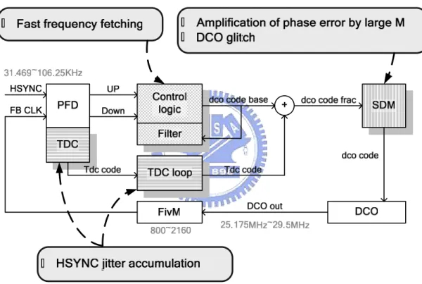
Fig. 3.1 The block diagram of proposed ADPLL, and the main targets of each block Fig. 3.1 shows the proposed Video capture phase lock loop block diagram. The Sigma-Delta Modulator (SDM), Time-to-Digital Converter (TDC), TDC loop, and digital filter are added to the basic PLL loop to solve the challenges in high multiplication factor ADPLL design. The ADPLL basic blocks contains Phase/ Frequency Detector (PFD), control logic, Digital-Controlled Oscillator (DCO), and frequency divider (FivM).
The HSYNC jitter effect is reduced by the digital filter, and the filter also speeds up the lock-time. The DCO design challenge is solved by control logic, include glitch problem and inconsistent DCO resolution problem.
The problem of large DCO resolution to track input clock phase is solved by Sigma Delta modulator (SDM). It is used to enhance the DCO equivalent resolution. The DCO glitch problem is also solved by SDM. The MUX type DCO is modified to help glitch problem and also to reduce power consumption. The additional TDC loop is applied to resolve the design challenge of the instantaneous jitter of HSYNC.
The working principle of proposed ADPLL is described as follow. UP and DOWN information is outputted from the PFD then sent into the control-logic. Subsequently, the TDC code is converted by TDC and sent into the TDC loop. The fractional DCO code is combined with the output from control-logic and the output of TDC loop and sent into SDM. The dithering is performed by SDM that produces the high rate DCO code to control the DCO. And then the FB_CLK is outputted by FivM and sent back the PFD.
3.1 Phase/Frequency Detector
3.1.1 Structure
The PFD [9] shown in Fig. 3.2 is used in our work. When the output clock (FB_CLK) leads the reference clock (REF_CLK), flagD presents a low signal and flagU keeps high. On the contrary, when FB_CLK lags REF_CLK, flagU presents a low pulse and flagD keeps high. Since the ADPLL controller only needs lead or lag signal, the digital pulse amplifier is used to minimize the dead zone of the PFD.
Fig. 3.3 Pulse amplifier structure [9]
The digital pulse amplifier [9] shown in Fig. 3.3 is applied to extend the low pulse-width of OUTU and OUTD, so the following D-flip-flops can detect it. This technique improves the dead-zone of PFD.
3.1.2 Simulation Result
Fig. 3.4 Simulation result of PFD circuit
Fig. 3.4 shows the simulation result of PFD. It is simulated by ULTRASIM S mode at SS corner. The simulation sweeps the phase error from FB_CLK leading
REF_CLK for 30ps to FB_CLK lagging REF_CLK for 40ps. The dead-zone of PFD is around 16ps. That is, when the phase error between REF_CLK and FB_CLK is less than ±16ps, flagU and flagD will both keep high and there is no leading or lagging information for ADPLL controller.
3.2 Digital Controlled Oscillator
3.2.1 Structure
In order to apply this ADPLL in all display modes (VGA, SVGA, XGA, SXGA, and UXGA), the operating period of DCO have to cover a very wide range from 6.173ns to 39.72ns. Therefore, a cell-based MUX-type DCO [14] is used in this design.
The MUX-type DCO has the advantage of minimum intrinsic delay and easy extension of the operating frequency range.
coarse-tuning stage
fine-tuning stage reset_
1'b1 coarse_sel[1] coarse_sel[2] coarse_sel[3] coarse_sel[0] MU X MU X MU X MU X
intr buf buf buf dummy
Fig. 3.5 A cell-based MUX type DCO structure
The structure of a MUX-type DCO with fine-tuning stage is shown in Fig. 3.5. This DCO contains two stages, which are coarse-tuning stage and fine-tuning stage. In coarse-tuning stage [14], one coarse-tuning delay contains a buffer delay (d_del) and a multiplexer delay (d_mux). The delay path is chose by coarse select signal (coarse_sel).
Fig. 3.6 Fine-tuning stage of DCO
In order to increase the frequency resolution of the DCO, a fine-tuning stage, as
shown in Fig.3.6, is adde fine-tuning delay cell is
composed of digitally controlled varactor
3.2.2 Solutions of Digital Controlled Oscillator Glitch
In order to produce a glitch-free-ADPLL, a modified MUX-type DCO is applied. e glitch problem
d before the coarse-tuning stage. The
(DCV) [10]. The schematic of the DCV cell is shown in top of Fig. 3.6. It utilizes the different gate capacitance of NAND gates controlled by different digital codes to build a digitally controlled varactor.
The coarse cell is modified from buffer to OR gate in order to solve the target-typ and also gain the benefit of saving power, as shown in Fig. 3.7. Since both of the target paths are always fixed at high, there is no glitch problem.
fine-tuning stage reset_ del[1] del[63] mout[2] 1'b1 mout[0] d_del d_mux d_mux d_del coarse_sel[0:63] mout[1] intr d_mux
coarse coarse dummy
en_[0] en_[62] 1'b0 dco_out del[0] del[1] mout[2] coarse_sel Safe region for changing path d_mux+d_control controller d_control No target-type glitch del[0]
Fig. 3.7 Modified DCO structure
Therefore, only original-type glitch problem has to be resolved, as long as the limitation of control delay is less than (d_fine + d_intr), the glitch will not occur.
3.2.3 Problem of Uniform Resolution
The coarse delay is determined by the number of OR gate and MUX gate. Moreover, the fine delay is determined by the number of load capacitor. Because the sources of delay are distinct, the PVT variation of delay is different. Therefore, it is difficult to design a uniform resolution DCO. Non-monotonic or large resolution would takes place and results in unstable loop tracking, as shown in Fig. 3.8.
0.5 1 1.5 4.5 5 5.5 6 coarse.fine code per iod( ns )
Non-expect large step
0.5 1 1.5 4.5 5 5.5 6 coarse.fine code per iod( ns ) Non-monotonic
Fig. 3.8 The difficult of uniform resolution in DCO code changing over stage In order to solve the monotonic issue, the delay range of fine-tuning stage is designed to be larger than one coarse-tuning step, and the special consideration of the design of the controller is describe in detail in section 3.3.
3.2.4 Simulation result
The DCO is simulated in ULTRASIM S mode. Fig. 3.9 shows the period of DCO output clock versus coarse code (0~127) when fine code is zero. The simulations in FF, TT, and SS corners are shown in (a), (b), and (c) respectively. In FF corner, the DCO period range is from 1.86ns to 40.29ns, and the DNL is ±0.158∆, the INL is ±0.103∆, where the ∆ is the ideal step. In TT corner, the DCO period range is from 2.63ns to 59.53ns, and the DNL is ±0.202∆, INL is ±0.107∆. In SS corner, DNL is ±0.019, INL is ±0.016, and DCO period range is from 4.18ns to 98.46ns.
0 20 40 60 80 100 120 140 -0.2 -0.1 0 0.1 0.2 s mode FF c: 0~127: dnl=+-0.158, inl=+-0.103 coarse code DN L(d el ta) 0 20 40 60 80 100 120 140 -0.2 -0.1 0 0.1 0.2 coarse code IN L(de lta) 0 20 40 60 80 100 120 140 0 0.5 1 1.5 2 2.5 3 3.5 4 4.5x 10 4 s mode FF c: 0~127
coarse step mean=302.64ps,max=353.00ps,min=257.40ps intr=1.86ns max period=40.29ns
coarse code
pe
rio
d(ps
)
(a) FF corner, DNL: ±0.158∆, INL: ±0.103∆, DCO period range: 1.86ns ~ 40.29ns
0 20 40 60 80 100 120 140 -0.4 -0.2 0 0.2 0.4 s mode TT c: 0~127: dnl=+-0.202, inl=+-0.107 coarse code DNL (d el ta ) 0 20 40 60 80 100 120 140 -0.1 0 0.1 0.2 0.3 coarse code IN L(del ta) 0 20 40 60 80 100 120 140 0 1 2 3 4 5 6x 10 4 s mode TT c: 0~127
coarse step mean=448.02ps,max=538.80ps,min=357.60ps intr=2.63ns max period=59.53ns
coarse code
peri
od(ps
)
(b) TT corner, DNL: ±0.202, INL: ±0.107, DCO period range: 2.63ns ~ 59.53ns
0 20 40 60 80 100 120 140 -0.02 -0.01 0 0.01 0.02 s mode SS c: 0~127: dnl=+-0.019, inl=+-0.016 coarse code DNL (d el ta ) 0 20 40 60 80 100 120 140 -0.02 -0.01 0 0.01 0.02 coarse code IN L(del ta) 0 20 40 60 80 100 120 140 0 1 2 3 4 5 6 7 8 9 10x 10 4 s mode SS c: 0~127
coarse step mean=742.35ps,max=756.80ps,min=728.60ps intr=4.18ns max period=98.46ns
coarse code
peri
od(ps
)
(c) SS corner, DNL: ±0.019, INL: ±0.016, and DCO period range: 4.18ns ~ 98.46ns Fig. 3.9 Simulation of DCO period versus coarse code 0 ~ 127
0 20 40 60 80 100 120 140 0 1 2 3 4 5 6 7 8 9 10x 10 4
s mode coarse code: 0~127
SS mean step=742.35ps,max step=756.80ps,min step=728.60ps intr=4.18ns max period=98.46ns TT mean step=448.02ps,max step=538.80ps,min step=357.60ps intr=2.63ns max period=59.53ns FF mean step=302.64ps,max step=353.00ps,min step=257.40ps intr=1.86ns max period=40.29ns
coarse code pe rio d(p s) SS TT FF
Fig. 3.10 Comparison of DCO period in PVT variation
Fig. 3.10 shows the DCO period versus coarse code in SS, TT, FF corner. The range covered in every corner is from 4.18ns to 40.29ns which can be applied from VGA to UXGA mode.
0 0.5 1 1.5 2 2.5 3 3.5 4 4.5 5 1000 2000 3000 4000 5000 6000 7000 8000 9000
s mode coarse:0~4 when coarse=0
SS fine step mean=17.20ps max=25.02ps min=5.34ps, range=1083.70ps cover=338.84ps TT fine step mean=11.48ps max=15.68ps min=4.06ps, range=723.54ps cover=272.86ps
FF fine step mean=8.68ps max=10.40ps min=2.20ps, range=546.54ps cover=244.62ps
coarse.fine code pe rio d( ps ) SS TT FF
Fig. 3.11 Simulation of DCO period of coarse code and fine code
Fig. 3.11 shows the period of DCO output clock versus coarse code (0~4) and fine code (0~63). The average step of fine stage delay is 8.68ps in FF corner, 11.48ps in TT corner, 17.20ps in SS corner. The average range of fine stage delay is 546.54ps in FF corner, 723.54ps in TT corner, 1083.70ps in SS corner. The range of fine stage is larger than one coarse delay step, and the overlap delay is 244.62ps in FF corner, 272.86ps in TT corner, and 338.84ps in SS corner.
3.3 Control Logic
3.3.1 State diagram
reset reset reset step=={1,0,0} cont=0 reset cont=0 step=={0,0,1} Frequency Searching Init cont=15 step={1,0,0} If(phase polarity) cont--; step={1,0,0}; Lock state lock=1 step={0,0,1} Coarse SAR Init step={8,0,0} SDM off TDC loop off reset If(phase polarity) step>>1; step={0,0,1} Fine&Fraction SAR Init step={0,32,0} SDM on If(phase polarity) step>>1; Phase tracking Init cont=127 TDC loop onstep={0,0,1} If(phase polarity) cont--; step={0,0,1}; Fig. 3.12 The finite state diagram of PLL controller
The state diagram of the controller is shown in Fig. 3.12. The control algorithm will influence the frequency lock time and phase tracking performance. In the design, the step code contains 7bits coarse-tuning code, 6bits fine-tuning code, and 8bits fraction-tuning code, and is expressed by {coarse code, fine code, fractional code}. The phase polarity is high as the PFD comparison result is changed.
phase clk dco code 8,0,0 4,0,0 2,0,0 1,0,0 step p_up p_down phase polarity filter ok XXXX 3d 39 3a Coarse SAR FS state A A A average code B B B C C
Fig. 3.13 Timing diagram in Coarse SAR state
The first state is Coarse SAR (successive approximation register) State. The initial step is {8,0,0} and the SDM and TDC-loop are turned off. In this state, only the coarse-tuning code will be changed. As shown in Fig. 3.13, when phase polarity (A), the step code will be divided by 2 to reduce the tuning-step (B), and the average code from filter will be reloaded to DCO control code (C) to speed up the frequency searching if the state of filter is ok.
phase clk dco code 1,0,0 step p_up p_down phase polarity 41 Frequency Searching state average code f e d c b a 9 8 7 6 5 4 3 2 1 0 38 39 40 42 43 44 42 41 40 41 40 cont
Fig. 3.14 Timing diagram in Frequency Searching state
When the step code is reduced to {1,0,0}, the control unit enters Frequency Searching State. The purpose of this state is to find the best coarse code. The step code is kept in {1,0,0} for 15 occurrences of phase polarity for filter to find an average coarse code, as shown in Fig. 3.14. After entering the Frequency Searching State, coarse code has been held to avoid the situation that coarse and fine contact with each other to cause non-monotonic or the worse resolution.
The third state is Fine & Fraction SAR State. The behavior of this stage is similar to the Coarse SAR State. The initial step code is {0,32,0}. Only fine-tuning code and fractional code will be changed in this state. After this state, the SDM is activated to dither the DCO fine code. The dithering working principle will be explained in SDM section.
When the step code is reduced to minimum step {0,0,1}, the ADPLL controller enters the Phase Tracking State. After this state, the TDC-loop is stimulated to
compensate the instant input jitter infection. After 128 times of frequency polarity in Phase Tracking State, the ADPLL is locked.
3.3.2 Digital Loop Filter
Fig. 3.15 PLL Frequency and Phase Tracking Procedure
Fig. 3.15 shows the DCO control code versus time. In Region I, the PLL controller changes the control code in large step in order to speed up frequency fetching and phase tracking. After entering Region II, the frequency of REF_CLK and FB_CLK are almost the same. The PLL controller decreases the tuning-step code to keep tracking the frequency and the phase of REF_CLK.
Owing to the HSYNC jitter, the PLL loop have to keep tracking and renewing the DCO control-code after PLL loop is locked, or the loop will be unstable and causing a noisy pixel clock. A digital loop filter is introduced to avoid the HSYNC jitter involved in the PLL loop which may cause large output jitter.
Therefore, the PLL controller sends the DCO control-code to the digital loop filter to calculate an average DCO control code (avg_dco_code). After PLL loop frequency is locked, the avg_dco_code carries the baseline frequency information. Then the DCO
control code is slightly tuned nearby avg_dco_code by PLL controller to keep the loop stable and to maintain the tracking of phase.
Filter Update FSM
T0 T1 T(M-1) TM T(M+K-1)
K New Inputs Summation
M
M: tap number of filter
avg_dco_code
K: number of new inputs dco_code
Fig. 3.16 Digital Loop Filter Block Diagram
Fig. 3.16 shows the block diagram of digital filter, K represents the number of new input DCO control code, and M is the number of wanted code of filter. The digital loop filter renews the value stored in the register according to un-ceased input DCO control code. The avg_dco_code for PLL controller will be added and calculated by T0 to T(M+1)
in registers.
When PLL is operating, 10 DCO control code will be stored in the digital loop filter registers. The maximum and minimum stored code will be replaced by new input DCO control code. The avg_dco_code is calculated by averaging the DCO control codes inside the filter except for the maximum and minimum ones, and then the avg_dco_code for baseline frequency is obtained.
When the phase polarity occurs, for example, from lead to lag, the PLL controller updates the avg_dco_code to the DCO control code to reduce the output phase error, and keep the stable PLL loop from input noise.
Moreover, the PLL loop with digital filter eases off the over-tracking situation and speed up the frequency lock speed. After the frequency is locked, it steadies output frequency by filtering the input jitter.
3.4 Dithering Technique
3.4.1 Dithering Theorem
n2 Δ P1+ n1+n2 ×Fig. 3.17 Dithering technique enhances period resolution
Fig. 3.17 shows how the use of high rate clock improves the equivalent DCO resolution [11][12]. The x axis is the DCO period and the y axis is time. Here, n1 cycles of period P1 and n2 cycles of period P1+Δ are mixed in one HSOUT period. The
equivalent pixel clock period is given by P1 n1+(P1+Δ) n1
n1+n2 × × =P1+n2 Δ n1+n2 × . The equivalent resolution is improved from Δ to
n1+n2 Δ
HSYNC Ideal Pixel clock Over-sampling Pixel clock Over-sampling Phase Error No over-sampling Pixel clock No over-sampling Phase Error M ∆/2 T+∆/2 T+∆/2 T+∆/2 T+∆/2 T+∆/2 T+∆/2 T+∆/2 T+∆/2 T T T T T T T T T T+∆ T T+∆ T T+∆ T T+∆ ∆/2 Fig. 3.18 Phase error reduction by dithering technique
Fig. 3.18 shows how to use over-sampling method to reduce the phase error. For example, the multiplication factor in the Figure is M, and DCO resolution is Δ. Assume the cycle of Ideal pixel clock is T + Δ / 2. In one HSYNC cycle, if all the periods of M pixel clock cycles are T, the phase error is accumulated to M×∆/2. If the periods of pixel clock are controlled by high-speed clock, that is, HSOUT is formed with a mix of T and T + Δ pixel clock periods, and then the phase error is controlled under Δ/2.
From the figure, another key point is that the high-speed pixel clock controller should averagely separate two kinds of different periods to minimize the pixel clock Phase error accumulation.
In order to reduce the complexity of circuits, Sigma-Delta Modulator (SDM) is applied to realize the dithering of DCO period.
3.4.2 Sigma Delta Modulator Overview
SDM is widely used in over-sampling data converter for its capability to push noise to high frequency. Then, the quantization noise can be removed by low pass filter. For ADC application, analog input is converted to digital output with enhanced resolution after passing through the sigma delta modulator. In a sufficiently long time period, the average of digital output will be much closer to the value of the analog input than that in an ADC without SDM. In Fractional-N PLL application, the multiplication factor can be considered as over-sampling a DC analog signal. For example, a non-integer multiplication factor of frequency can be generated by more than one divide ratio dithering at over-sampling rate.
In this design, a SDM is applied to dither the DCO control code to minimize the phase error in phase tracking procedure. Since the multiplication factor of Video Capture PLL is from 800~2160, this architecture intrinsically produces a clock in slow rate and a clock in high rate. This characteristic of Video Capture PLL is used to improve the DCO equivalent resolution by sampling slow rate signal by high rate clock.
Fig. 3.19 First-order SDM Structure
A first order SDM is shown in Fig. 3.19 [13]. The ∆ block is digital differential block and ∑ block is digital integration. Inside the block, Z-1 is the digital delay cell. A
delayed y signal is sent into ∆ block to generate the difference between output y and input x, then v is generated from ∑ block by integrating the difference. After v is quantified by the quantification, output y is refreshed.
From the discussion in time domain
( ) ( 1) ( 1) ( )
x n −y n− +v n− =v n
When n is substituted for 1, 2, 3, to N, the equations are generated below
(1) (0) (0) (1) (2) (1) (1) (2) (3) (2) (2) (3) ... ( ) ( 1) ( 1) ( ) x y v v x y v v x y v v x N y N v N v N − + = − + = − + = − − + − =
The equation below is generated by summing up the equations above 1 1 0 ( ) (0) ( ) ( ) N N n n v N v x n y n − = = − =
∑
−∑
From the assumption of x is a slow rate signal, and v converges all the time, the approximate equation is generated below.
1 0
( ) (0) 1
lim lim lim ( )
N N N N n v N v x y n N N − →∞ →∞ →∞ = − = −
∑
That is ( ) Average y → xSigma delta modulator improves the equivalent resolution in digital application, but it requires another high speed over-sampling clock. In the video capture ADPLL application, the large multiplication factor provides a high over-sampling ratio (OSR) and over-sampling rate in nature. The enhancement of equivalent resolution can be achieved with no penalty.
3.4.3 Sigma Delta Modulator Structure and Working
Principle
Fig. 3.20 Modified first-order SDM
In the proposed Video Capture PLL, a modified first order SDM is applied, as shown in Fig. 3.20, so that the area of SDM can be reduced in this structure and the cycle-to-cycle jitter can be minimized.
Fig. 3.21 The working principle of SDM [11]
The working principle of SDM is shown in Fig. 3.21. After Fine & Fraction SAR State, the fractional code is generated from PLL controller which is triggered by slow-rate phase clock, and then sent into the SDM which is triggered by high-rate pixel
clock. After that, SDM generates a series of high-rate changing integer codes according to the fraction code and is used to control the DCO so the non-integer DCO resolution can be performed.
3.4.4 Simulation Result
Fig. 3.22 shows the simulations of the jitter performance with the assumptions of 1ps DCO resolution and ideal input HSYNC clock (no input jitter). Simulations with 0 bits, 5 bits, 6 bits fractional codes are shown respectively.
0 200 400 600 800 1000 1200 -80 -60 -40 -20 0 20 40 60
80 UXGA HYSNC and HSOUT: Phase Drift Over Time
Time Index P ha se D rift ( ns) (a) 0 bits fractional code
0 200 400 600 800 1000 1200 -2 -1.5 -1 -0.5 0 0.5 1 1.5
2 UXGA HYSNC and HSOUT: Phase Drift Over Time
Time Index P ha se D rift ( ns)
0 200 400 600 800 1000 1200 -0.2 -0.15 -0.1 -0.05 0 0.05 0.1 0.15
0.2 UXGA HYSNC and HSOUT: Phase Drift Over Time
Time Index P ha se D rift ( ns)
(c) 6 bits fractional code
Fig. 3.22 Simulation with different fractional code bits
Table 3.1 Summary of peak-to-peak phase drift in different fractional code bits
0 bits 5 bits 6 bits
Peak-to-Peak Phase drift (ns) ±67.406 ns ±1.573 ns ±0.165 ns
From the simulation, the performance of phase drift is ±67.406 ns with 0 bits fractional code, ±1.573 ns with 5 bits, and ±0.165 ns with 6bits, as shown in Table 3.1. The phase drift is improved by adding the fractional bit counts substantially, that is, when the fractional bit counts are increased, the equivalent resolution is better.
3.5 Time-to-Digital Converter Loop
Although the proposed Video Capture ADPLL with SDM achieves the high multiplication factor and low output jitter when the HSYNC is clean. The tuning step is too small to track the phase jitter of a noisy HSYNC.
When jitter is observed in reference clock, the circuit can not track it fast enough which leads to phase error accumulation. In order to maintain the high resolution of DCO and the capability of tracking the reference clock jitter, the sigma-delta ADPLL needs an additional TDC loop to overcome this phase variation.
The TDC loop is designed to affect the present dco_code_frac without accumulation. Hence, the ADPLL can compensate the phase jitter of HSYNC rapidly and avoid the noise of reference clock from interfering the stable loop and cause false lock.
In the Fig. 3.1, the dco_code_base varies one fractional code or jumps to average code after lock-in. The property of dco_code_base is stable and varies slightly. It contains the main frequency information of reference clock. The cp_code is converted by TDC from the phase error between reference and feedback clock, which varies with the phase drift that caused by HSYNC jitter.
3.5.1 Working Principle
In TDC-loop, the phase error is quantified by TDC, and then the PLL controller tunes the DCO-code according to TDC-code for the phase error compensation caused by instant HSYNC jitter. Besides, the TDC-code is only used to influence DCO-code once, and it will not change the average frequency. Therefore, the TDC-loop compensates large HSYNC jitter at once, and avoids instability caused by input noise injection.
Fig. 3.23 shows the working principle of TDC. The phase drift is detected by PFD and quantified by TDC to TDC-code. The TDC-code is multiplied by TDC-loop-gain and sent into SDM-DCO. Then the tuning-code will be averagely scattered over the flowing pixel clock by SDM. For this reason, before the next HSYNC rising-edge, the phase error caused by HSYNC jitter this time has been compensated.
3.5.2 Structure
(a)
(b)
TDC structure is shown in Fig. 3.24. Because of the performance of input jitter compensation is strongly dependent on the TDC resolution, a traditional TDC [15] is used in the proposed ADPLL.
For the lead and lag information, two duplicate TDC is used, the advantages of this structure are small resolution and small dead zone. The simulation result is listed in the Table tdc_performance. In SS corner, the resolution is 100ps, and the dead zone of detection is 190ps.
Table 3.2 Summary of the TDC performance
resolution dead zone range
SS 100ps <190ps can’t be detected 6400ps
FF 44ps <70ps can’t be detected 2816ps
3.5.3 Simulation Result
3.5.3.1 Discussion of Time-to-Digital Converter Loop
In Fig. 3.25 left half, the x axis is the input jitter and the y axis is the phase error (ns). The simulation without TDC is shown in the left half of Fig. 3.25 (a), the phase error reaches 6ns at 1.2ns jitter. The simulation with TDC is shown in the left half of Fig. 3.25 (b), the phase error is reduced to 1.6ns at the same case.
The percentage of ideal pixel clock period versus input jitter is shown in the right half of Fig. 3.25 (a) and Fig. 3.25 (b). Since the period of ideal pixel clock in UXGA mode is only 6.173ns, the phase error have to be smaller than 33% of ideal pixel clock period. From the simulation result, the performance in UXGA mode and 1.2ns input jitter is reduced from 80% to 22 % by adding the TDC loop.
0 0.2 0.4 0.6 0.8 1 1.2 1.4 0 10 20 30 40 50 60 70 80
TDC off HYSNC and HSOUT Phase Drift over jitter
jitter(ns) P has e D rif t [ % of out put c loc k ] VGA(800) SVGA(1056) XGA(1344) SXGA(1688) UXGA(2160) 0 0.2 0.4 0.6 0.8 1 1.2 1.4 0 1 2 3 4 5
6 TDC off HYSNC and HSOUT Phase Drift over jitter
jitter(ns) Ph as e D rif t (n s) VGA(800) SVGA(1056) XGA(1344) SXGA(1688) UXGA(2160)
(a) Simulation without TDC, the maximum phase drift is 6ns (78%)
0 0.2 0.4 0.6 0.8 1 1.2 1.4 0 0.2 0.4 0.6 0.8 1 1.2 1.4 1.6
1.8 TDC on HYSNC and HSOUT Phase Drift over jitter
jitter(ns) P has e D rif t (ns ) VGA(800) SVGA(1056) XGA(1344) SXGA(1688) UXGA(2160) 0 0.2 0.4 0.6 0.8 1 1.2 1.4 0 5 10 15 20 25
TDC on HYSNC and HSOUT Phase Drift over jitter
jitter(ns) Ph as e D rift [% o f o utp ut c lo ck ] VGA(800) SVGA(1056) XGA(1344) SXGA(1688) UXGA(2160)
(b) Simulation with TDC, the maximum phase drift is 1.6ns (22%)
Fig. 3.25 Simulation the phase error of PLL with and without TDC in VGA to UXGA The detailed simulation data is listed in Table 3.3. The column represents different input jitter (0ps ~ 1.2ns) and the row represents different view modes (VGA to UXGA). The shadowed statics are simulated without TDC-loop and the unshadowed ones are simulated with TDC-loop and the unit is in percentage.
Table 3.3 Phase Error in Different Operation Modes (phase error unit: %)
% VGA SVGA XGA SXGA UXGA
0.3348 0.6242 1.5470 3.4938 2.6730 Jitter 0ps 0.1158 0.1120 0.0910 0.8262 0.9639 1.8114 2.9731 6.5422 11.0106 19.9422 Jitter 200ps 0.7527 1.4045 2.1612 3.0564 4.6656 4.7329 8.7713 12.0672 19.3752 31.0716 Jitter 500ps 1.7132 2.3729 3.6367 6.2424 9.5742
10.8077 13.2890 26.4354 34.8192 63.3744 Jitter 1000ps 3.4012 5.0859 7.2345 11.5398 18.0711 14.6494 18.3709 31.6484 53.1036 78.1002 Jitter 1200ps 4.0809 6.2163 9.2397 12.8628 21.6270
3.5.3.2 Discussion of TDC Loop Gain
The result in the above section is simulated on the basis of ideal TDC gain. However, in reality, the TDC resolution and the DCO resolution are both affected by PVT variation. The simulation below is to discuss the effect of non-ideal TDC gain.
The ideal TDC gain is calculated as follow,
IdealPixelPeriod=CoarseResolution CoarseCode+FineResolution FineCode+Epixel Epixel Multiplication=Ehsync=TdcResolution TdcCode+
Ehsync 1 TdcCode TdcResolution
TuneCode= Multiplication FineResolution M E ul tdc × × × × × × ≈ 1 tiplication FineResolution TdcResolution = TdcCode FineResolution Multiplication TdcResolution IdealTdcGain= FineResolution Multiplication × × × ×
From the equation above, Epixel is the difference between ideal pixel clock period and DCO clock period and then Ehsync is amplified from Epixel by multiplication factor. Etdc is the difference between actual phase error and TDC detected phase drift.
If the Ehsync (actual phase error) can be uniformly scattered over the flowing pixel clock period, the Ehsync can be almost eliminated (except for Etdc) before next HSYNC rising-edge.
However, the TDC delay-cell is different from DCO delay-cell so the DCO-code cannot be adjusted by TDC-code directly. The best DCO tuning-code has to be converted from TDC code. The relation between best tuning code and TDC code is calculated in the equation, and the Etdc is ignored.
The ideal TDC gain is decided by TDC-resolution, DCO-resolution and Multiplication-factor. The multiplication-factor is a constant (decided by view-mode) but the resolution of DCO and TDC are changed in PVT variation. In the following simulation, the assumptions are 4ps DCO resolution, 100ps TDC resolution, 6bits fractional code, and the ideal TDC gain being around 1~2 as listed in Table 3.4.
Table 3.4 Ideal TDC Gain for Different Operation Mode TDC resolution 100ps, fine tune resolution 4ps/64
Mode VGA(800) SVGA XGA SXGA UXGA(2160)
Ideal gain 2 1.56 1.19 0.95 0.76
In order to verify the influence of TDC-gain, a PLL model is established in MATLAB, and simulations with different jitter models and different TDC-gain are made. In the following simulations, ratio factor is defined by the variation rate of HSYNC jitter. HSYNC jitter varies fast with small ratio factor, and vice versa. The equation of ratio factor is given by
fs ratio=
fm
HSYNC Jitter=Pk-Pk Input Jitter sin(2π fm # of period)× × ×
In the equation, fs is defined as sampling frequency used in MATLAB simulation.
0 2 4 6 8 10 1.3332 1.3334 1.3336x 10 4 # of period per io d ( ns )
ratio=1.7 HSYNC period
0 2 4 6 8 10 1.3332 1.3334 1.3336x 10 4 # of period per iod ( ns ) ratio=8.7 HSYNC period
In Fig. 3.26, the x axis is the numbers of HSYNC period and the y axis is the period of HSYNC. The HSYNC period varies fast in ratio1.7 and varies slow in ratio 8.7. The peak-to-peak jitters of two conditions are the same, but the cycle-to-cycle jitter of ratio1.7 is much bigger than that of ratio 8.7.
0 5 10 15 20 25 30 35 40 45 50 -10 -5 0 5 10 # of period jit te r (n s)
TDCnoM PhaseError(p-p)=+-7.067(ns) gain=0.0 ratio=19.7
HSYNC jitter HSOUT jitter Phase Drift Filter output jitter
(a) ratio=19.7 0 5 10 15 20 25 30 35 40 45 50 -4 -2 0 2 4 # of period jit te r (n s)
TDCnoM PhaseError(p-p)=+-3.402(ns) gain=0.0 ratio=10.7
HSYNC jitter HSOUT jitter Phase Drift Filter output jitter
(b) ratio=10.7 0 5 10 15 20 25 30 35 40 45 50 -4 -2 0 2 4 # of period jit te r (n s)
TDCnoM PhaseError(p-p)=+-2.674(ns) gain=0.0 ratio=8.7
HSYNC jitter HSOUT jitter Phase Drift Filter output jitter
(c) ratio=8.7
Fig. 3.27 Simulation without TDC
Fig. 3.27 shows the simulation of ADPLL loop jitter performance without TDC-loop. The peak-to-peak value of HSYNC jitter is set to ±1.2ns in all simulations, and the ratio is set to 19.7, 10.7 and 8.7 respectively in (a), (b) and (c). In the Fig., the circle marked line is HSYNC jitter, the upward-pointing triangle marked line is
HSOUT jitter, the asterisk marked line is phase error between HSYNC and HSOUT, and the point marked line is the output jitter of digital loop filter.
The simulation results show that when the HSYNC jitter varies more slowly, the accumulated phase error is larger. The phase error is up to ±7.076ns when ratio is equal to 19.7, and phase error is ±2.674 when ratio is 8.7.
0 5 10 15 20 -2 -1 0 1 2 # of period jit te r ( ns )
TDCnoM PhaseError(p-p)=+-0.957(ns) gain=0.5 ratio=2.7
HSYNC jitter HSOUT jitter Phase Drift Filter jitter 0 5 10 15 20 -2 -1 0 1 2 # of period jit te r ( ns )
TDCnoM PhaseError(p-p)=+-1.766(ns) gain=0.5 ratio=19.7
HSYNC jitter HSOUT jitter Phase Drift Filter jitter (a) gain=0.5 0 5 10 15 20 -2 -1 0 1 2 # of period jit te r ( ns )
TDCnoM PhaseError(p-p)=+-1.309(ns) gain=1.0 ratio=2.7
HSYNC jitter HSOUT jitter Phase Drift Filter jitter 0 5 10 15 20 -2 -1 0 1 2 # of period jit te r ( ns )
TDCnoM PhaseError(p-p)=+-1.103(ns) gain=1.0 ratio=19.7
HSYNC jitter HSOUT jitter Phase Drift Filter jitter (b) gain=1.0 0 5 10 15 20 -5 0 5 # of period jit te r ( ns )
TDCnoM PhaseError(p-p)=+-1.964(ns) gain=2.0 ratio=2.7
HSYNC jitter HSOUT jitter Phase Drift Filter jitter 0 5 10 15 20 -2 -1 0 1 2 # of period jit te r ( ns )
TDCnoM PhaseError(p-p)=+-1.239(ns) gain=2.0 ratio=19.7
HSYNC jitter HSOUT jitter Phase Drift Filter jitter
(c) gain=2.0
Fig. 3.28 Simulation with different TDC gain and different HSYNC jitter ratio Fig. 3.28 shows the discussions of phase drift with different TDC gain and different HSYNC jitter ratio. The ADPLL phase error performance is simulated in different TDC gain, which are (a) 0.5 times, (b) 1 times, and (c) 2 times of ideal TDC gain respectively. The Fig.s in the left are simulated with 2.7 ratio factor (fast rate of jitter variation), and the ratio factor in the right half of the Figures are set to 19.7 (slow rate).
From the simulation result, when the HSYNC jitter varies slowly, the performance of ADPLL with larger TDC gain is better than which with the smaller ones. However, when the HSYNC jitter varies fast, the ADPLL with the smaller TDC gain is better. Hence, when the HSYNC with same direction occurs successively, the accumulation of phase drift can be restrained by TDC loop. But when the HSYNC jitter varies between plus and minus rapidly, there is no contribution for the phase error of the TDC loop. Fortunately, there is not much accumulation of phase error in this case.
0 5 10 15 20 0 1 2 3 4 5 6 7 8 pp ph as e e rror (n s) ratio
HSYNC jitter=1.20ns pp, filter tank=8 Peak to Peak Phase Error VS. ratio
gain=0.0 gain=0.5 gain=1 gain=2
Fig. 3.29 Phase error vs. HSYNC jitter ratio with different TDC gain
The Fig. 3.29 shows the peak-to-peak phase error versus ratio with different TDC gain. From the results, in the large ratio situation, the accumulation of phase error can be reduced by ADPLL loop with large TDC gain. However, in the small ratio situation, additional phase error is introduced by large TDC gain. Therefore, a suitable TDC gain is important to the performance of input jitter compensation.
0 5 10 15 20 25 30 35 40 45 50 -1 -0.5 0 0.5 1 jit te r (n s) # of period
HSYNC from computer, SXGA mode, period pp=+-0.950ns
Fig. 3.30 Measurement of the practical HSYNC jitter
In order to find a suitable TDC gain, a real HSYNC jitter is measured from PC through D-sub probe and shown in Fig. 30. We use discrete Fourier transform to find the correspond ratio, and simulate in the MATLAB ADPLL model, a better performance is achieved when TDC gain about 0.5~1.
Chapter 4 Chip Implementation
4.1 Chip Layout View
VDD P VSSP VD DC VSSC HSYN CD FBC L KD HSYN C EN _CK OUT VDD P VSSP RESET DIVM _M OD E[0] DIVM _M OD E[1] DIVM _M OD E[2] DIVM _M OD E[3] VSSP
Fig. 4.1 Floor plan and I/O plan
Fig. 4.1 shows the expected floor plan, 32 PADs is used in this chip, and the I/O PADs description is shown below
Table 4.1 I/O PAD description
input bits function
RESET 1 set chip to initial
HSYNC 1 input clock
EN_CKOUT 1 enable pixel clock to output
EN_TDC_LOOP 1 enable TDC loop to work
set the bits number of SDM fractional code
value multiplication factor
0 8 bits fractional code
1 6 bits fractional code
2 4 bits fractional code
SD_MODE 2
3 0 bits fractional code (SDM off)
set the multiplication factor of ADPLL
value multiplication factor
1 VGA 800 2 SVGA 1056 3 XGA 1344 4 SXGA 1688 5 UXGA 2160 6 32 7 64 8 128 9 256 10 512 11 1024 12 2048 13 4096 DIVM_MODE 4 14 5600
output bits function
HSYNCD 1 reference clock
FB_CLK 1 feedback clock
CKOUT 1 pixel clock
LOCK 1 phase lock signal
dcoclk
domain
phaseclk
domain
pfd
tdc
D
C
O
Fig. 4.2 Layout of proposed ADPLL
Fig. 4.2 shows the final layout view of the proposed ADPLL. The area of the core is 900 ×1000 μm . The pfdtdc block contains the Phase/Frequency detector and time-to-digital converter (TDC). The phaseclk domain block contains the PLL control-logic and TDC loop which operates at slow rate clock phase clock. The dco domain block contains the sigma-delta modulator (SDM) and the frequency divider which operates at high speed clock pixel clock. Finally, the DCO block is placed beside the dcoclk dcomain.
4.2 Overall Simulation
4.2.1 Simulations in Verilog
For verilog simulation consideration, we assume that the TDC resolution is 100ps, DCO resolution is 18ps, and the jitter model of HSYNC is normal distribution.
VGA SVGA XGA SXGA UXGA 0 0.5 1 1.5 2 2.5 3 3.5 4 mode P has e D rif t pk t o pk (ns )
notdc HSYNCjitter=0.0ns DCOresolution=18ps HYSNC and HSOUT: Phase Drift peak to peak SDM 6bits
SDM 8bits
(a) Phase error (ns) between HSYNC and HSOUT
VGA SVGA XGA SXGA UXGA 0 10 20 30 40 50 60 70 mode P has e D rif t pk t o pk (% of ideal pi xel c loc k)
notdc HSYNCjitter=0.0ns DCOresolution=18ps HYSNC and HSOUT: Phase Drift peak to peak SDM 6bits
SDM 8bits
(a) Phase error (% of ideal pixel clock period) between HSYNC and HSOUT Fig. 4.3 Verilog simulation with 6 bits and 8 bits fractional code
The phase drift performance of proposed ADPLL is simulated in 6bits and 8bits fractional code with different view mode (VGA to UXGA). The assumption of the simulation in Fig. 4.3 is no HSYNC jitter. From the Fig. 4.3, the phase drift is 3.7ns (60%) in UXGA mode in 6bits fractional code, and it is reduced to less than 1ns (15%) in 8bits fractional code.
VGA SVGA XGA SXGA UXGA 0 0.5 1 1.5 2 2.5 3 3.5 4 4.5 mode P has e D rif t pk t o pk (ns )
sd8 HSYNCjitter=1.2ns DCOresolution=18ps HYSNC and HSOUT: Phase Drift peak to peak TDC off
TDC on
(a) Phase error (ns) between HSYNC and HSOUT
VGA SVGA XGA SXGA UXGA 0 10 20 30 40 50 60 mode P has e D rif t pk t o pk (% of ideal pi xel c loc k)
sd8 HSYNCjitter=1.2ns DCOresolution=18ps HYSNC and HSOUT: Phase Drift peak to peak TDC off
TDC on
(b) Phase error (% of ideal pixel clock period) between HSYNC and HSOUT Fig. 4.4 Verilog simulation with on/off TDC loop
When the jitter of HSYNC is set to 1.2ns normal distribution, the phase drift performance of the ADPLL with 8bits fractional code is simulated with on/off TDC loop in different view mode (VGA to UXGA), as shown in Fig. 4.4. The upward-pointing triangle shows the curve with TDC off and the downward-pointing triangle shows the curve with TDC on. From the Fig., the phase drift is 3.4ns (55%) when TDC is off in UXGA mode, and it is reduced to 1.369ns (22%) by the compensation of instant HSYNC jitter when TDC is on.
4.2.2 Simulations in AMS
Because of the low rate HSYNC, for example, 75kHz in UXGA, and high switching speed of output clock, the simulation time is considerable. A mixed mode simulator AMS is used here to improve the simulation time.
VGA SVGA XGA SXGA UXGA 0
0.5 1 1.5 2
sd8bits tdc HSYNC jitter=1.2ns DCOresolution=18ps HYSNC and HSOUT: Phase Drift peak to peak
mode 1.429 1.4745 1.502 1.246 1.2775 P ha se D rift p k to p k( ns )
VGA SVGA XGA SXGA UXGA 0 5 10 15 20 25 30 35 40
sd8 tdc HSYNC jitter=1.2ns DCOresolution=18ps HYSNC and HSOUT: Phase Drift peak to peak
mode 3.5975 5.898 9.7628 13.4572 20.695 P ha se D rif t pk t o pk (% of pi xel c loc k pe riod )
(b) Phase error (% of ideal pixel clock period) between HSYNC and HSOUT Fig. 4.5 AMS simulation with 8bits fractional code and TDC loop
Fig. 4.5 shows the simulation by AMS simulator, the PFD and TDC are sourced to spice file, and the other are set to verilog. The assumption of DCO resolution is 18ps, and the TDC loop is on, SDM with 8bits fractional code, and 1.2ns HSYNC normal distribution jitter. The total performance is controlled in 1.275ns (20.695%) in UXGA mode.
4.2.3 Post-layout Simulation
A simulation of the design circuit after LPE in test mode (6MHz input, 192MHz output, 32 multiplication factor) is simulated by ULTRASIM MS mode. The result is better than the result in same condition simulated by VERILOG model.
Chapter 5 Conclusion and
Future Work
In this thesis, a fast phase-tracking cell-based ADPLL with large frequency multiplication factor for video application is proposed. It has good portability for different process, and is easily integrated in SOC because no external RC components are required.
A modified 2-stage MUX-type DCO with 13-bit control code is realized to cover the wide operating range from 25MHz to 230MHz, and eliminate the occurrence of glitch. The controller and digital loop filter speed up the frequency tracking, and avoid the instability by input jitter injection. The design problem of uniform DCO resolution is also solved by the controller.
A first order SDM is applied to enhance DCO equivalent resolution from 18ps to 70.3fs, so the difficulty for achieving large multiplication factor is overcome. The phase error is controlled under 1ns at 2160 multiplication factor.
In order to compensate the instant HSYNC jitter, a TDC loop is proposed to affect the DCO control through SDM dithering technique. The phase error is controlled under 1.3ns when assuming HSYNC jitter to be 1.2ns and normally distributed at 2160 multiplication factor.
Finally, the chip is implemented in TSMC 0.18μm 1P5M standard CMOS process. The power consumption of post-layout simulation is 6.7mW at 6MHz input and 192MHz output frequency, and the core size is 1000x1000um2.
A measure result will be demonstrated after the accomplishment of chip manufacture. One of the most important topics for further improvement of the ADPLL performance is to automate the adjustment of TDC-loop gain according to the input jitter form to immunize the system from PVT variation. Another topic of further work is to modify the TDC and DCO structure to keep the resolution and reduce the chip area. Simplification of the controller is also an important topic in the further design.
Reference
[1] H. Marie and P. Belin, “R, G, B acquisition interface with linelocked clock generator for flat panel display,” IEEE J. Solid-State Circuits, vol. 33, no. 7, pp.1009-1023, July 1998.
[2] W. E. Rodda, E. R. Campbell, D. J. Sauer, and W. T. Mayweather, “Full CMOS video line-locked phase-locked loop system”, IEEE Trans. Consumer Electronics, vol. 39, No. 3, pp.496-503, Dec. 1993.
[3] “Video Capture PLL,” Analog Bits Inc., Datasheet Datasheet.
[4] “Low Refresh Rate PLL IP core targeted at Video and Flat Panel Display,” CEVA
Inc., Datasheet.
[5] J. B. Begueret, Y. Deval, O. Mazouffre, A. Sparato, P. Fouillat, E. Benoit, and J. Mendoza, “Clock generator using factorial DLL for video applications”, Proc. of
IEEE Custom Integrated Circuits Conf. (CICC), pp. 485-488, May 2001.
[6] J. Lin, B. Haroun, and T. Foo, “A PVT tolerant 0.18 MHz to 600 MHz self-calibrated digital PLL in 90-nm CMOS process,” Tech. Dig. of IEEE
International Solid-State Circuit (ISSCC), , Feb. 2004, vol. 541, pp. 488-489.
[7] “Monitor Timing Specifications,” VESA and Industry Standards and Guidelines for Computer Display Monitor Timing VESA and Industry Standards and Guidelines

![Fig. 2.3 Jitter versus multiplication factor at fixed 240-MHz output [8]](https://thumb-ap.123doks.com/thumbv2/9libinfo/8470837.183533/18.892.160.638.551.1039/fig-jitter-versus-multiplication-factor-fixed-mhz-output.webp)

![Fig. 3.2 The modified 3-state PFD architecture [9]](https://thumb-ap.123doks.com/thumbv2/9libinfo/8470837.183533/25.892.183.718.930.1115/fig-modified-state-pfd-architecture.webp)
