國 立 交 通 大 學
電信工程學系
碩士論文
擴展式二重濾波器及三階橫斷式濾波器
The Extended Doublet and Third-Order
Transversal Filter
研究生:紀佩綾
指導教授:張志揚 博士
擴展式二重濾波器及三階橫斷式濾波器
The Extended Doublet and Third-Order Transversal
Filter
研 究 生:紀佩綾 Student:Pei-Ling Chi
指導教授:張志揚 博士 Advisor:Dr. Chi-Yang Chang
國 立 交 通 大 學
電 信 工 程 系
碩 士 論 文
A Thesis
Submitted to Department of Communication Engineering
College of Electrical and Computer Engineering
National Chiao Tung University
in partial Fulfillment of the Requirements
for the Degree of Master of Science
in
Communication Engineering
June 2006
Hsinchu, Taiwan, Republic of China
擴展式二重濾波器及三階橫斷式濾波器
學生:紀佩綾 指導教授:張志揚 博士
國立交通大學電信工程學系
摘 要
本論文基於解析濾波器的結構及針對合成、診斷濾波器的電子參數(也就是 耦合矩陣)之電腦輔助設計提出了一套快速實現濾波器的方法。這種設計過程可 以避免花費大量的時間在電路的調整上。在擴展式二重濾波器(extended doublet filter)的架構下,我們實現了二種不同 需求的濾波器電路。其中一個是為了擁有高度選擇性,而另一個則是針對在通帶 具有平坦的群延遲響應。群延遲已經被證明和訊號的失真有關。如同展示在論文 中的數據,我們成功地消除了將會使群延遲表現變差的非預期耦合,而量測的結 果更證實了讓通帶的群延遲變化小於 0.5 奈秒的可行性。 對於三階的橫斷式濾波器(transversal filter),我們建立一套快速估計相關電 路參數的法則。我們定義了一個新參數-特性阻抗的比例,並且發現了它在實現 濾波器的重要性。這個方法只需少次數的疊代計算,此歸因於它的快速收斂特 性。在數值分析及量測結果高度一致下,更驗證了這個方法的實用及有益性。 為了要配合現今通訊系統的需求,我們讓這些濾波器都設計在中心頻 2.4 千 兆赫,以便可以容易的整合在 IEEE 802.11 b/g、ISM 和藍芽的系統中。
The Extended Doublet and Third-Order
Transversal Filter
Student: Pei-Ling Chi Advisor: Dr. Chi-Yang Chang
Department of Communication Engineering
National Chiao Tung University
Abstract
This thesis presents the fast realization of filter configurations based on analytical analysis of the proposed structures and CAD method for synthesis and diagnosis of the electrical parameters of the filter, i.e., the coupling matrix. The design procedures avoid consuming large amount of time in circuit tuning.
In the extended doublet coupling scheme, we realize two categories of filter requirements. One is for high skirt selectivity. The other is for in-band flat group delay, which has been demonstrated in association with the signal distortion. As exhibited in the thesis, we successfully eliminate the unwanted coupling that would degrade the performance of in-band group delay. The measured data validate the possibility with the variation of in-band group delay less than 0.5 ns.
As for the 3rd-order transversal filter, we establish an algorithm for quick estimation of the related electrical parameters to be determined. We define a new parameter, the impedance ratio r, and observe its importance in realization of the filter. This algorithm only involves a few of iterations due to its fast convergence. Good agreement between analytical computation and measured results indicates that such approach is practical and useful.
In order to meet the requirement in nowadays communication systems, we design these filters with center frequency at 2.4 GHz for easy integration in the environments of IEEE 802.11 b/g, ISM, and Bluetooth standards.
Acknowledgment
The author especially appreciates Prof. Chang for his continuous instruction and consideration. His inspiration and guidance not only build up my foundation for microwave circuit design but also assist my completeness of this thesis. I also would like to thank the lab senior, Ching-Ku Liao, for his enthusiastic explanation and suggestion.
Finally, I am grateful to have all the support from my family. Your absolute backup and thoughtfulness have made what I am today. I would like to dedicate this work to my whole family members.
Contents
Abstract………...i Abstract in English……….ii Acknowledgment………..iii Contents……….………iv List of Figures………...vi List of Tables……….ix Chapter 1 Introduction………...1 Chapter 2 Theory………52.1 General Coupling Matrix for Coupled-Resonator Filters…………..……….5
2.1.1 Loop Equation Formulation……….………..…5
2.1.2 Mathematical Definition of the Coupling Coefficient and Its Physical Explanation……….8
2.2 Lowpass Prototype Filters and Frequency/Element Transformation…………10
2.2.1 Lowpass Prototype Filters and Elements………...10
2.2.2 Immittance Inverters………11
2.2.3 Frequency and Element Transformations………..….13
2.3 The Governing Equations of the Two-Port Network, and the Relationship between Coupling Coefficients and Resonant Frequencies/External Quality Factors………..17
2.3.1 The N+2 Extended Coupling Matrix, Network Representation, and Governing Equations of the Network Circuit with N Coupled Lossless Resonators………18
2.3.2 The Relationship between Coupling Coefficients and Resonant
Frequencies/External Quality Factors………..21
2.4 Equivalent Expressions for Parallel Coupled-Lines Using Inverter……….….22
2.5 The Provision of Design Flow Based on the Numerical Computation……….24
Chapter 3 Extended Doublet………26
3.1 Introduction of the Extended Doublet……….……….26
3.2 Introduction of an Analytical Approach for Synthesis Based on the Chosen Layout………28
3.3 Simulation and Implementation for the Extended Doublet……….32
3.3.1 The Extended Doublet for Selectivity Requirement………...32
3.3.2 The Extended Doublet for Flat-Group-Delay Requirement………35
Chapter 4 Third-Order Transversal Filter……….42
4.1 Introduction of the 3rd-Order Transversal Filter………42
4.2 Introduction of an Analytical Approach for Synthesis Based on the Chosen Layout………..43
4.3 Sensitivity Analysis of the 3rd-Order Transversal Filter………..48
4.4 Simulation and Implementation for the 3rd-Order Transversal Filter……….48
Chapter 5 Conclusions……….58
List of Figures
Figure 1.1 (a) Typical coupling structure of CQ filters. (b) Typical coupling structure of CT filters………1 Figure 1.2 The coupling and routing scheme of the extended doublet………..2 Figure 2.1.1 Equivalent circuit of n-coupled resonators for loop-equation formulation……….5 Figure 2.1.2 General coupled RF/microwave resonators where resonator 1 and 2 can be different in structure and have different resonant frequencies………..9 Figure 2.2.1 Lowpass prototype filters for all-pole filters with a ladder network structure and its dual……….11 Figure 2.2.2 Lowpass prototype filters modified to include immittance inverters…..13 Figure 2.2.3 Lowpass prototype to bandpass transformation: basic element transformation………..15 Figure 2.2.4 Bandpass filters using immittance inverters………16 Figure 2.2.5 Generalized bandpass filters (including distributed elements) using immittance inverters……….17 Figure 2.3.1 The network representation of the two-port n-coupled resonator filter..19 Figure 2.3.2 The coupling and routing scheme of the extended doublet………20 Figure 2.3.3 Typical I/O coupling structures for coupled resonator filters. Left part: tapped-line coupling. Right part: coupled-line coupling……….22 Figure 2.4.1 Parallel coupled striplines and their electric parameters……….23 Figure 2.4.2 An equivalent circuit of parallel coupled lines using a J-inverter……...23 Figure 2.5.1 The methodology of filter implementation in our thesis……….25
Figure 3.1.1 The coupling and routing scheme of the extended doublet with coupling
coefficients indicated for different filter applications……….26
Figure 3.1.2 An ideal distortionless system……….27
Figure 3.2.1 The doublet with even- and odd-mode analysis………..29
Figure 3.2.2 Configuration under odd-mode analysis for the doublet……….30
Figure 3.2.3 Configuration under even-mode analysis for the doublet………31
Figure 3.3.1 Circuit and layout of the doublet for selectivity requirement…………..33
Figure 3.3.2 Frequency response of the doublet for selectivity requirement………...34
Figure 3.3.3 The final layout and simulation results (under lossless condition) of the extended doublet for selectivity requirement………..34
Figure 3.3.4 The photograph of the extended doublet for selectivity requirement…..35
Figure 3.3.5 Measured and simulated S parameters of the extended doublet for selectivity requirement……….35
Figure 3.3.6 The layout and simulation results (under lossless condition) of the 1st proposed extended doublet for flat-group-delay requirement………..37
Figure 3.3.7 The photograph of the 1st proposed extended doublet for flat-group-delay requirement………..37
Figure 3.3.8 Measured and simulated S parameters of the 1st proposed extended doublet for flat-group-delay requirement……….38
Figure 3.3.9 Measured and simulated group delay of the 1st proposed extended doublet for flat-group-delay requirement……….38
Figure 3.3.10 The layout and simulation results (under lossless condition) of the 2nd proposed extended doublet for flat-group-delay requirement………..39
Figure 3.3.11 The photograph of the 2nd proposed extended doublet for flat-group-delay requirement………39 Figure 3.3.12 Measured and simulated S parameters of the 2nd proposed extended
doublet for flat-group-delay requirement……….40 Figure 3.3.13 Measured and simulated group delay of the 2nd proposed extended doublet for flat-group-delay requirement……….40 Figure 3.3.14 The measured data of the 2nd proposed extended doublet for flat-group-delay requirement………41 Figure 4.1.1 The coupling and routing scheme of the 3rd-order transversal filter……42 Figure 4.2.1 The 3rd-order transversal filter with even- and odd-mode analysis…….44 Figure 4.2.2 Configuration under odd-mode analysis for the 3rd-order transversal filter………..45 Figure 4.2.3 Configuration under even-mode analysis for the 3rd-order transversal filter………..46 Figure 4.4.1 The iteration flow of the impedance ratio r acquisition………..53
Figure 4.4.2 Circuit and layout of the 3rd-order transversal filter in case 1…………54 Figure 4.4.3 Frequency response of the 3rd-order transversal filter for case 1……….54 Figure 4.4.4 Circuit and layout of the 3rd-order transversal filter for case 2…………55 Figure 4.4.5 Frequency response of the 3rd-order transversal filter for case 2……….55 Figure 4.4.6 The layout and simulation results (under lossless condition) of the 3rd-oredr transversal filter……….56 Figure 4.4.7 The photograph of the 3rd-order transversal filter………56 Figure 4.4.8 Measured and simulated S parameters of the 3rd-order transversal filter.57
List of Tables
Table 2.3.1 Coupling matrix for the extended doublet……….20 Table 3.3.1 Specification and positions of finite TZs in lowpass prototype of the extended doublet for selectivity requirement………...32 Table 3.3.2 Coupling matrix of the extended doublet for selectivity requirement…...32 Table 3.3.3 Specification and positions of finite TZs in lowpass prototype of the extended doublet for flat-group-delay requirement……….36 Table 3.3.4 Coupling matrix of the extended doublet for flat-group-delay requirement………..36 Table 4.3.1 Sensitivity investigation on the coupling coefficients with respect to the variations of dimensions in the physical parameters………49 Table 4.4.1 Specification and positions of finite TZs in lowpass prototype of the 3rd-order transversal filter……….51 Table 4.4.2 Coupling matrix of the 3rd-order transversal filter………52 Table 4.4.3 The iteration process for the impedance ratio r ………..52
Chapter 1 Introduction
Although filter design theory has been well established, one systematic approach based on numerical computation, which aids to accelerate the implementation of the desired filter structure, is still far to complete. Over the last decades, many scholars and researchers have intended to diagnose the filter with numerical analysis from the coupling matrix [1]-[6]. By developing the relationship between the electrical parameters (each element in the coupling matrix) and the physical parameters in the configuration [7], it is simple to realize the filter in no time. In this thesis, we devise filter structures with the help from numerical syntheses and diagnoses, and the design flow based on that method would be described in detail.
High performance microstrip filters with high selectivity and linear in-band phase response has been investigated extensively for the demanding requirement in communication systems. Some well-known topologies such as cascade quadruplet
Figure 1.1 (a) Typical coupling structure of CQ filters. (b) Typical coupling structure of CT filters.
(CQ) and cascade trisection (CT) have been successfully realized using microstrip. Figure 1.1 illustrates typical coupling structures of CQ and CT filters, where each node represents a resonator, the solid lines indicate the main coupling path, and the broken lines denote the cross coupling. M is the coupling coefficient between the ij
resonators i and j , and Q and e1 Q are the external quality factors in association en
with the input and output coupling, respectively. However, compared with the conventional CQ topology, the coupling scheme of the extended doublet proposed in this paper has the superior properties to that one [8].
Figure 1.2 The coupling and routing scheme of the extended doublet.
Traditional quadruplet section is restricted to generate two symmetric transmission zeros (TZs) either in the real or imaginary axis [9]. The extended doublet has the flexibility of exhibiting both symmetric and asymmetric responses. Another important feature is the fact that when moving the TZs in the complex plane, the signs
of all coupling coefficients in the matrix remain unchanged. It implies that we can realize filter specification with skirt selectivity (TZs at the real frequency axis) or linear phase response (TZs at the real axis of the complex plane) [10] in the same structure by only adjusting the relative magnitudes in the corresponding coupling coefficients. In this thesis, we demonstrate that the extended doublet has better in-band phase response than that of the quadruplet. Furthermore, the extended doublet is only a 3rd-order filter and thus may result in less loss with the same number of TZs as a CQ filter. Figure 1.2 shows the coupling and routing scheme of the extended doublet.
Transversal filters are one of the simplest building blocks for generating the finite TZs, especially for the second-order case (i.e., doublet). Many papers have used these coupling schemes for filter implementations [11], [12], but not yet developed any analytical approach to systematically practice the transversal filters. We have attempted to establish one algorithm contributing to the fast realization of the 3rd-order transversal filter and successfully validate the possibility of such method from the simulation solver and experiment. Also, sensitivity analysis has been incorporated in the design procedure and that issue has attracted some researchers to pay attention to [13], [14]. Sensitivity determination is an important step regarding the manufacturing tolerance. From these sensitivities, acceptable bounds on the errors in the entries of the coupling matrix can be determined before an attempt is made to implement the network. Based on these results, the actual implementation can be either pursued or abandoned.
The operating frequency of the proposed filter configurations is chosen at 2.4 GHz for accommodating these devices to the frequency usage of nowadays communication standards, such as the ISM band, IEEE 802.11 b/g, and Bluetooth wireless technology. In consideration of the ease of fabrication and low cost, the
entire circuits were fabricated on the printed circuit board (PCB) with dielectric constant εr of 10.2 and thickness of 25 mil.
Chapter 2 Theory
2.1 General Coupling Matrix for Coupled-Resonator Filters
2.1.1
Loop Equation Formulation
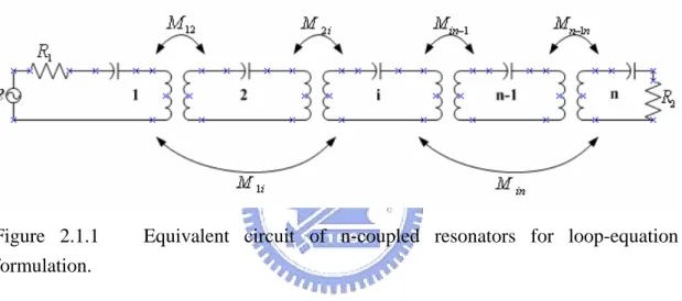
[1]Figure 2.1.1 Equivalent circuit of n-coupled resonators for loop-equation formulation.
Shown in Figure 2.1.1 is an equivalent circuit of n-coupled resonators, which includes the inductors, resistors, and capacitors. e represents the voltage source and s
ij
M (as will be explained clearly later) denotes the coupling coefficient between
resonators i and j . Using the voltage law, which is one of Kirchhoff’s two circuit laws and states that the algebraic sum of the voltage drops around any closed path in a network is zero, we can write down the loop equations for the circuit of Figure 2.1.1
1 1 1 12 2 1 1 21 1 2 2 2 2 1 1 2 2 2 1 1 0 1 0 n n s n n n n n n n R j L i j L i j L i e j C j L i j L i j L i j C j L i j L i R j L i j C ω ω ω ω ω ω ω ω ω ω ω ω ⎛ ⎞ + + − − = ⎜ ⎟ ⎝ ⎠ ⎛ ⎞ − +⎜ + ⎟ − = ⎝ ⎠ ⎛ ⎞ − − +⎜ + + ⎟ = ⎝ ⎠ L L M L (2.1)
in which Lij =Lji represents the mutual inductance between resonators i and j ,
and the all loop currents are supposed to be in the clockwise direction. This set of equations can be represented in the matrix form
1 1 12 1 1 21 2 2 2 1 1 1 n n n R j L j L j L j C j L j L j L j C j L ω ω ω ω ω ω ω ω ω + + − − − + − − L L M M M M 1 2 2 2 0 0 1 s n n n n i e i i j L R j L j C ω ω ω ⎡ ⎤ ⎢ ⎥ ⎢ ⎥ ⎡ ⎤ ⎡ ⎤ ⎢ ⎥ ⎢ ⎥ ⎢ ⎥ ⎢ ⎥ ⎢ ⎥ ⎢ ⎥= ⎢ ⎥ ⎢ ⎥ ⎢ ⎥ ⎢ ⎥ ⎢ ⎥ ⎢ ⎥ ⎢ ⎥⎣ ⎦ ⎣ ⎦ ⎢ − + + ⎥ ⎢ ⎥ ⎣ ⎦ M M L (2.2) or
where [Z] is an n n× impedance matrix.
For simplicity, let us first consider a synchronously tuned filter. In this case, all resonators resonate at the same frequency, namely the mid-band frequency of filter
0 1
LC
ω = , where L=L1 =L2 = L and Ln C =C1 =C2 = L . The impedance Cn
matrix in (2.2) can be expressed by
[ ]
Z ω0L FBW[ ]
Z−
= ⋅ ⋅ (2.3) where
0
FBW = Δωω is the fractional bandwidth of the filter, and
[ ]
Z−
is the normalized impedance matrix, which in the case of synchronously tuned filter is given by
[ ]
1 1 12 0 0 0 2 21 0 0 1 0 1 1 1 1 n n n L R L p j j L FBW L FBW L FBW L L j p j L FBW L FBW Z L j ω ω ω ω ω ω ω ω ω ω ω − + − ⋅ − ⋅ ⋅ − ⋅ − ⋅ = − L L M M M M 2 2 0 0 1 1 Ln R j p L FBW L FBW L FBW ω ω ω ⎡ ⎤ ⎢ ⎥ ⎢ ⎥ ⎢ ⎥ ⎢ ⎥ ⎢ ⎥ ⎢ ⎥ ⎢ ⎥ ⎢ ⋅ − ⋅ + ⎥ ⎢ ⋅ ⎥ ⎣ M ⎦ (2.4) with 0 0 1 p j FBW ω ω ω ω ⎛ ⎞ = ⎜ − ⎟ ⎝ ⎠the complex lowpass frequency variable. It should be noticed that
0 1 for 1, 2 i ei R i L Q ω = = (2.5) 1 e
Q and Q are the external quality factors of the input and output resonators, e2
respectively. Define the coupling coefficient as
ij ij L M L = (2.6) and assuming 0 1 ω
ω ≈ for a narrow-band approximation, we can simplify (2.6) as
[ ]
12 1 1 21 2 1 2 2 1 1 n e n n n e p jm jm q jm p jm Z jm jm p q − ⎡ + − − ⎤ ⎢ ⎥ ⎢ ⎥ − − ⎢ ⎥ = ⎢ ⎥ ⎢ ⎥ ⎢ ⎥ − − + ⎢ ⎥ ⎣ ⎦ L L M M M M L (2.7)where q and e2 q are the scaled external quality factors e2
for 1, 2
ei ei
q =Q ⋅FBW i = (2.8) and m denotes the so-called normalized coupling coefficient ij
ij ij M m FBW = (2.9) In the case that the coupled-resonator circuit of Figure 2.1.1 is asynchronously tuned, and the resonant frequency of each resonator, which may be different, is given by
0i 1 i i L C
ω = , the coupling coefficient of asynchronously tuned filter is defined as
for ij ij i j L M i j L L = ≠ (2.10)
It can be shown that (2.7) becomes
[ ]
11 12 1 1 21 22 2 1 2 2 1 1 n e n n n nn e p jm jm jm q jm p jm jm Z jm jm p jm q − ⎡ + − − − − − − = − − + − L L M M M M L ⎤ ⎢ ⎥ ⎢ ⎥ ⎢ ⎥ ⎢ ⎥ ⎢ ⎥ ⎢ ⎥ ⎢ ⎥ ⎣ ⎦ (2.11)The normalized impedance matrix of (2.11) is almost identical to (2.7) except that it has the extra entries m to account for asynchronous tuning. Finally, we could have ii
a unified formulation for a n-coupled resonator filter regardless of whether the couplings are magnetic or electric or even the combination of both. The normalized impedance matrix
[ ]
Z−
(or the normalized admittance matrix
[ ]
Y−
) may be expressed as a general one:
[ ] [ ] [ ] [ ]
A = q + p U − j m (2.12)where
[ ]
U is the n n× identity matrix,[ ]
q is an n n× matrix with all entries zero, except for 111 1 e q q = and 2 1 nn e q q
= ,
[ ]
m is the so-called general coupling matrix, which is an n n× reciprocal matrix (i.e., mij =mji) and is allowed to have nonzero diagonal entries m for an asynchronously tuned filter. ii2.1.2 Mathematical Definition of the Coupling Coefficient and Its
Physical Explanation
[1]can be different in structure and can have different self-resonant frequencies (see Figure 2.1.2), may be defined on the basis of the ratio of coupled energy to stored energy, i.e., 1 2 1 2 2 2 2 2 1 2 1 2 E E dv H H dv k E dv E dv H dv H dv ε μ ε ε μ μ − − − − − − − − • • = + × ×
∫∫∫
∫∫∫
∫∫∫
∫∫∫
∫∫∫
∫∫∫
(2.13) where E − and H −represent the electric and magnetic field vectors, respectively, and we now use the more traditional notation k instead of M for the coupling coefficient. Note that all fields are determined at resonance, and the volume integrals are over all affected regions with permittivity of ε and permeability of μ. The first
Figure 2.1.2 General coupled RF/microwave resonators where resonator 1 and 2 can be different in structure and have different resonant frequencies.
term on the right-hand side represents the electric coupling and the second term the magnetic coupling. It should be remarked that the interaction of the coupled resonators is mathematically described by the dot operation of their space vector fields, which allows the coupling to have either positive or negative sign. A positive sign would imply that the coupling enhances the stored energy of uncoupled resonators, whereas a negative sign would indicate a reduction. Therefore, the electric
and magnetic coupling could either have the same effect if they have the same sign, or have the opposite effect if their signs are opposite. Obviously, the direct evaluation of the coupling coefficient from (2.13) requires knowledge of the field distributions and performance of the space integrals.
2.2 Lowpass Prototype Filters and Frequency/Element
Transformation
2.2.1 Lowpass Prototype Filters and Elements
[1], [15], [16]A lowpass prototype filter is in general defined as the lowpass filter whose element values are normalized to make the source resistance or conductance equal to one, denoted by g0 = , and the cutoff angular frequency to be unity, denoted by 1
1
c
Ω = (rad/s). For example, Figure 2.2.1 demonstrates two possible forms of an n-pole lowpass prototype for realizing an all-pole filter response, including Butterworth, Chebyshev, and Gaussian responses. Either form may be used because both are dual from each other and give the same response. It should be noted that in Figure 2.2.1, gi for i to n represent either the inductance of a series inductor or the capacitance of a shunt capacitor; therefore, n is also the number of reactive elements. If g1 is the shunt capacitance or the series inductance, then g0 is defined as the source resistance or the source conductance. Similarly, if gn is the shunt capacitance or the series inductance, gn+1 becomes the load resistance or the load conductance. Unless otherwise specified these g-values are supposed to be the inductance in henries, capacitance in farads, resistance in ohms, and conductance in mhos.
Figure 2.2.1 Lowpass prototype filters for all-pole filters with a ladder network structure and its dual.
This type of lowpass filter can be served as a prototype for designing many practical filters with frequency and element transformations. This will be addressed in the next section.
2.2.2 Immittance Inverters
[1], [15], [16]Immittance inverters are either impedance or admittance inverters. An idealized impedance inverter is a two-port network that has a unique property at all frequencies, i.e., if it is terminated in an impedance Z2 on one port, the impedance Z1 seen looking in at the other port is
2 1 2 K Z Z = (2.14) where K is real and defined as the characteristic impedance of the inverter. As can be seen, if Z2 is inductive/conductive, Z1 will become conductive/inductive.
Impedance inverters are also known as K -inverters. The ABCD matrix of ideal impedance inverters may generally be expressed as
0 1 0 jK A B C D jK ⎡ ⎤ ⎡ ⎤ ⎢ ⎥ = ⎢ ⎥ ⎢± ⎥ ⎣ ⎦ ⎢ ⎥ ⎣ ⎦ m (2.15) Likewise, an ideal admittance inverter is a two-port network that exhibits such a property at all frequency that if an admittance Y2 is connected at one port, the admittance Y1 seen looking in the other port is
2 1 2 J Y Y = (2.16) where J is real and called the characteristic admittance of the inverter. Admittance inverters are also referred as J-inverters. In general, ideal admittance inverters have the ABCD matrix
1 0 0 A B jJ C D jJ ⎡ ± ⎤ ⎡ ⎤ ⎢ ⎥ = ⎢ ⎥ ⎢ ⎥ ⎣ ⎦ ⎢ ⎥ ⎣m ⎦ (2.17) An ideal immittance inverter is a lossless, reciprocal, frequency-independent, two-port network. As indicated, inverters have the ability to shift impedance or admittance levels depending on the choice of K or J parameters. Making use of these properties enables us to convert a filter circuit composed of the ladder network to an equivalent form with immittance inverters incorporated that would be more convenient for implementation.
For example, the two common lowpass prototype structures in Figure 2.2.1 may be converted into the forms shown in Figure 2.2.2.
Figure 2.2.2 Lowpass prototype filters modified to include immittance inverters.
2.2.3 Frequency and Element Transformations
[1], [15], [16]So far, we have only considered the lowpass prototype filters, which have a normalized source resistance/conductance g0=1 and cutoff frequency Ω =1. To c obtain frequency characteristic and element values for practical filters based on the lowpass prototype, one may apply frequency and element transformation, which will be addressed in this section.
The frequency transformation, which is referred to as frequency mapping, is required to map a response such as Chebyshev response in the lowpass prototype frequency domain Ω to that in the frequency domain ω in which a practical filters response such as lowpass, highpass, bandpass, and bandstop. The frequency transformation will have an effect on all the reactive elements accordingly, but no effect on the resistive elements.
In addition to the frequency mapping, impedance scaling is also required to accomplish the element transformation. The impedance scaling will remove the g0=1
normalization and adjust the filter to work for any value of the source impedance denoted by Z0. For our formulation, it is convenient to define an impedance scaling factor γ0 as 0 0 0 0 0 0 0
being the resistance being the conductance
for g for g Z g g Y
γ
⎧ ⎪ ⎨ ⎪ ⎩ = (2.18) where 0 0 1 Y Z= is the source admittance. In principle, applying the impedance scaling upon a filter network in such a way that
0 0 0 0 L L C C R R G G γ γ γ γ → → → → (2.19)
has no effect on the response shape.
Assume that a lowpass prototype response is to be transformed to a bandpass response having a passband ω2 − , where ω1 ω1 and ω2 indicate the passband-edge angular frequency. The required frequency transformation is
0 0 c FBW ω ω ω ω ⎛ ⎞ Ω Ω = ⎜ − ⎟ ⎝ ⎠ (2.20a) with 2 1 0 0 1 2 FBW ω ω ω ω ω ω − = = (2.20b)
where ω0 denotes the center angular frequency and FBW is defined as the fractional bandwidth. If we apply this frequency transformation to a reactive element
g of the lowpass prototype, we have
0 0 1 cg c g j g j FBW j FBW ω ω ω ω Ω Ω Ω → + (2.21)
which implies that an inductive/capacitive element g in the lowpass prototype will transform to a series/parallel LC resonant circuit in the bandpass filter. The elements for series LC resonator in the bandpass filter are
0 0 0 0 1 c s s c L g FBW FBW C g γ ω ω γ ⎛ Ω ⎞ = ⎜ ⎟ ⎝ ⎠ ⎛ ⎞ = ⎜ Ω ⎟ ⎝ ⎠
for g representing the inductance (2.22a)
where the impedance scaling has been taken into account as well. Similarly, the element for parallel LC resonator in the bandpass filter are
0 0 0 0 c p p c g C FBW FBW L g ω γ γ ω ⎛ Ω ⎞ = ⎜ ⎟ ⎝ ⎠ ⎛ ⎞ = ⎜ Ω ⎟ ⎝ ⎠
for g representing the capacitance (2.22b)
The frequency/element transformation in this case is shown in Figure 2.2.3.
Figure 2.2.3 Lowpass prototype to bandpass transformation: basic element transformation.
lowpass filter networks in Figure 2.2.2 can easily be transformed to the bandpass filter networks by applying the element transformations described in this section. For instance, Figure 2.2.4 illustrates two bandpass filters using immittance inverters.
Figure 2.2.4 Bandpass filters using immittance inverters.
Two important generalizations, shown in Figure 2.2.5, are obtained by replacing the lumped LC resonators by distributed circuits [17]. Distributed circuits can be microwave cavities, microstrip resonators, or any other suitable resonant structures. In the ideal case, the reactances or susceptances of the distributed circuits should equal those of the lumped resonators at all frequencies. In practice, they approximate the reactances or susceptances of the lumped resonators only near resonance. Nevertheless, this is sufficient for narrow band filter. For convenience, the distributed resonator reactance/susceptance and reactance/susceptance slope are made equal to their corresponding lumped-resonator values at band center. For this, two quantities, called the reactance slope parameter and susceptance slope parameter, respectively, are introduced. The reactance slope parameter for resonators having zero reactance at center frequency ω0 is defined by
( )
0 0 2 dX x d ω ω ω ω ω = = (2.23) where X( )
ω is the reactance of the distributed resonator. In the ideal case, thesusceptance slope parameter for resonators having zero susceptance at center frequency ω0 is defined by
( )
0 0 2 dB b d ω ω ω ω ω = = (2.24) where B( )
ω is the susceptance of the distributed resonator. It can be shown that thereactance slope parameter of a lumped LC series resonator is ω0L, and the susceptance slope parameter of a lumped LC parallel resonator is ω0C. Thus, replacing ω0Lsi and ω0Cpi with the general terms x and i b , as defined by (2.23) i
and (2.24), respectively, results in the corresponding values for the distributed circuits shown in Figure 2.2.5.
Figure 2.2.5 Generalized bandpass filters (including distributed elements) using immittance inverters.
2.3 The Governing Equations of the Two-Port Network, and
the Relationship between Coupling Coefficients and
Resonant Frequencies/External Quality Factors
2.3.1 The
N
+
2
Extended Coupling Matrix, Network
Representation, and Governing Equations of the Network Circuit
with
N
Coupled Lossless Resonators
[1], [2], [4]It was mentioned in [3] that, although the polynomial synthesis procedure was capable of generating N TZs for an N th-degree network, that a maximum of only
2
N− finite-position zeros could be realized by the N×N coupling matrix. This excluded some useful filtering characteristics, including those that required multiple input/output couplings, which have been finding applications recently [18].
In this section, we introduce the N +2 folded coupling matrix, which overcomes some of the shortcomings of the conventional N×N coupling matrix. The N+2 or “extended” coupling matrix has an pair of extra rows at top and bottom and an pair of extra columns at left and right. The extra rows and columns surround the “core” N×N coupling matrix, which carry the input and output couplings from the source and load terminations to resonator nodes in the core matrix. The N+2 matrix has two significant advantages, as compared with the conventional coupling matrix.
z Multiple input/output couplings may be accommodated, i.e., couplings may be made directly from the source/load to internal resonators, in addition to the main input/output couplings to the first/last resonator in the filter circuit. z Fully canonical filtering functions, i.e., Nth- degree characteristics with
N finite-position TZs may be synthesized.
[ ] [
A = Ω −U jR+M]
(2.25)where
[ ]
R is an (N+ ×2) (N+2) matrix whose nonzero entries are11 (N 2),(N 2) 1
R =R + + = ,
[ ]
U is similar to the (N+ ×2) (N + identity matrix except 2)11 (N 2),(N 2) 0
U =U + + = , and
[ ]
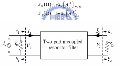
M is the (N + ×2) (N+2) symmetric coupling matrix.A network representation of two-port n-coupled resonator filter is shown in Figure 2.3.1, where V , 1 V and 2 I , 1 I are the voltage and current variables at the 2
filter ports, and the wave variables are denoted by a , 1 a , 2 b , and 1 b . After simple 2
calculation, it can be shown that the scattering parameters are given by
( )
( )
1 21 ( 2 ),1 1 11 11 2 1 2 N S j A S j A − + − ⎡ ⎤ Ω = − ⎣ ⎦ ⎡ ⎤ Ω = + ⎣ ⎦ (2.26)Figure 2.3.1 The network representation of the two-port n-coupled resonator filter.
Now, we further relate the TZs in lowpass prototype to the N +2 coupling matrix [19]. Since the transmission coefficient S is directly proportional to 21 ⎡⎣A−1⎤⎦ ,
the TZs can be found by letting 1
(N 2),1
A−
+
⎡ ⎤
⎣ ⎦ equal to zero. From Linear Algebra, we know 1 1 ( ) det( ) T A cof A A − ⎡ ⎤ = ⎣ ⎦ (2.27)
where cof A is the matrix of cofactors from ( )
[ ]
A . Therefore, the finite-position TZs are the roots of cofactor C1,(N+2) of[ ]
A .Design Example
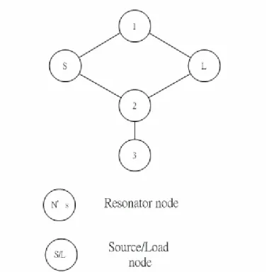
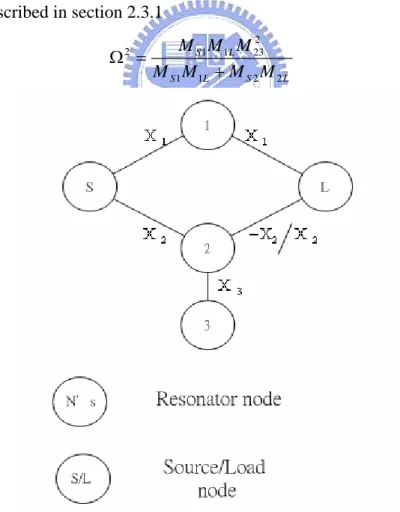
Figure 2.3.2 The coupling and routing scheme of the extended doublet.
Table 2.3.1 Coupling matrix for the extended doublet.
S 1 2 3 L S M S1 MS2 1 M S1
Ω
M 1L 2 MS2Ω
M 23 M2 L 3 M 32Ω
L M 1L M2 LSince M =23 M , we can derive the TZs in the lowpass prototype that are 32
located in the square roots of
2 2 1 1 23 1 1 2 2 S L S L S L M M M M M M M Ω = + (2.28) From (2.28), it is easy to realize that by controlling the values of coupling coefficients between resonators or source/load and resonators, the TZs could be placed as desired.
2.3.2 The Relationship between Coupling Coefficients and Resonant
Frequencies/External Quality Factors
[1], [7]The individual resonant frequency of each resonator in the circuit can also be established in association with the diagonal elements in the coupling matrix as follows: 0(1 ) for 1, , 2 ii i M FBW f = f − • i= L (2.29) n
where FBW and f are the fractional bandwidth and center frequency of the filter, 0
respectively.
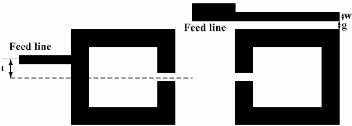
Before developing the formulation for the normalized quality factor, we first introduce the typical input/output (I/O) coupling structures used for coupled resonator filter. Two common I/O coupling structures for coupled microstrip resonator filters, namely the tapped line and the coupled line structures, are shown with the microstrip open-loop resonator, though other types of resonators may be used (see Figure 2.3.3). For the tapped line coupling, usually a 50 ohm feed line is directly tapped onto the I/O resonator, and the coupling or the external quality factor is controlled by the tapping position t , as indicated in the left part of Figure 2.3.3. For example, the smaller is the
t , the closer is the tapped line to a virtual grounding of the resonator, which results in
structure in the right part of Figure 2.3.3 can be found from the coupling gap g and the line width w. Normally, a smaller gap and a narrower line result in a stronger I/O coupling or a smaller external quality factor of the resonator.
Figure 2.3.3 Typical I/O coupling structures for coupled resonator filters. Left part: tapped-line coupling. Right part: coupled-line coupling.
For the quality factor of interest, we can derive that such formulae exist in the lowpass prototype , 2 , 2 1 1 ext S Si ext L iL q M q M = =
for resonator i coupled with source or load (2.30)
2.4 Equivalent Expressions for Parallel Coupled-Lines Using
Inverter
[20]Figure 2.4.1 shows the distributed coupling circuit applied to a stripline parallel-coupled BPF. The electric parameters of this circuit are expressed by even- and odd-mode impedance Z0e,Z , and electric coupling angle 0o θ . In the case of a
necessary to distinguish the coupling angles as θ0e and θ0o to obtain a strict analysis. However, this difference has little difference on the coupling strength, and thus here we consider θ0e =θ0o = for simplicity. θc
Figure 2.4.1 Parallel coupled striplines and their electric parameters.
For easy to directly synthesize the BPF, we introduce an equivalent circuit composed of two single lines and an admittance inverter, which we treated as an ideal coupling circuit without frequency dependency, as shown in Figure 2.4.2.
Figure 2.4.2 An equivalent circuit of parallel coupled lines using a J-inverter.
By equalizing the ABCD matrices of the parallel striplines and its equivalent circuit, we can obtain the following equations for Z and 0e Z , 0o
2 0 0 0 2 2 0 0 1 csc 1 cot c e c J J Y Y Z Z J Y θ θ ⎛ ⎞ ⎛ ⎞ +⎜ ⎟ +⎜ ⎟ ⎝ ⎠ ⎝ ⎠ = ⎛ ⎞ − ⎜ ⎟ ⎝ ⎠ (2.31) 2 0 0 0 2 2 0 0 1 csc 1 cot c o c J J Y Y Z Z J Y θ θ ⎛ ⎞ ⎛ ⎞ −⎜ ⎟ +⎜ ⎟ ⎝ ⎠ ⎝ ⎠ = ⎛ ⎞ − ⎜ ⎟ ⎝ ⎠ (2.32)
These equations are generalized expressions for parallel-coupled lines with arbitrary coupling length. For the case of a quarter-wavelength coupling, substituting
2
c π
θ = into (2.31) and (2.32) gives
2 0 0 0 0 1 e Z J J Z Y Y ⎛ ⎞ = + + ⎜ ⎟ ⎝ ⎠ (2.33) 2 0 0 0 0 1 o Z J J Z Y Y ⎛ ⎞ = − + ⎜ ⎟ ⎝ ⎠ (2.34) Equations (2.31) and (2.32) will be largely employed in the practical filter implementation in next chapters.
2.5 The Provision of Design Flow Based on the Numerical
Computation
[1]-[6]As mentioned in the beginning of chapter one, we have utilized the method of numerical analysis to help implement the filter circuits with optimization on the coupling matrix synthesis and diagnosis, it is better to provide the readers with the design flow based on this well-developed and systematic approach for clarity and further research investigation. The design flow is illustrated in the Figure 2.5.1 as following:
Chapter 3 Extended Doublet
3.1 Introduction of the Extended Doublet
[8]As illustrated in Figure 3.1.1 (only direct coupling shown), the extended doublet is a third order filter with the capability of realizing skirt selectivity or in-band linear phase response (shifting the finite-position TZs) only by adjusting the relative coupling magnitude between the corresponding resonators without sign alteration. This property can be concluded by observing the governing equation of the extended doublet, as described in section 2.3.1
2 2 1 1 23 1 1 2 2 S L S L S L M M M M M M M Ω = + (3.1)
Figure 3.1.1 The coupling and routing scheme of the extended doublet with coupling coefficients indicated for different filter applications.
Figure 3.1.1 also indicates the magnitude and sign of each main coupling path to express the following issue. In [10], it describes two classes of filters that have quite distinct applications. They are distinguished by the location of their TZs (attenuation poles), which, in the case of the first class, are at real frequencies, and in the case of the second class are at imaginary frequencies (i.e., on the real axis of the complex frequency plane). The TZs may be realized by cross coupling a pair of nonadjacent elements of the filter, negatively to give real-frequency TZs, positively to give real-axis zeros. The first type of filter gives improved skirt attenuation performance, and the second gives improved passband delay characteristics compared with the ordinary Chebyshev filter. Therefore, in this chapter, we will pay attention to implementing these two filter performances.
Figure 3.1.2 An ideal distortionless system.
Before we progress to the next step, it is necessary to point out the definition of the group delay and the importance of it to give the flat group delay (or linear phase response) in the communication systems. From communication theory, an ideal distortionless system is described as
( )
(
0)
y t = •A x t−t (3.2) where x t
( )
is the input signal to the channel and y t( )
is the output signal from the channel. A and t are the channel gain and delay, respectively. After performing 0( )
( )
j2 ft0Y f = •A X f •e− π (3.3) Thus, for an ideal distortionless communication channel, the output signal differs from the input signal in the magnitude with scale A and the phase delay 2 ftπ 0 in the frequency domain. The transfer function H f in the frequency domain of the ( ) ideal distortionless system is
( )
j2 ft0H f = Ae− π (3.4) With the definition of group delay,
( )
1( )
2 f f f δϕ τ π δ = − (3.5) where ϕ( )
f is the phase of the transfer function. Using (3.5), the group delay of the distortionless system is equal to t , which is a constant. Therefore, it is important to 0keep the in-band frequency response of the filter with flat (constant) group delay or linear phase response for minimizing the unwanted channel distortion.
3.2 Introduction of an Analytical Approach for Synthesis
Based on the Chosen Layout
After given the specification and determining the filter order, coupling routine, and positions of finite-position TZs, we have to choose the suitable filter structure for implementation. For the doublet subcircuit of the extended doublet, we take advantage of the configuration proposed in [11] with the even- and odd-mode analysis to fast realize the doublet. This structure is shown in Figure 3.2.1.
If a network is symmetrical, it is convenient for network analysis to bisect the symmetrical network into two identical halves with respect to its symmetrical interface. In this stage, the design procedure for the doublet based on the even- and
odd-mode analysis is ready to be addressed in detail.
Figure 3.2.1 The doublet with even- and odd-mode analysis.
Design Procedure for Doublet
Assuming that the resonant frequencies of the odd- and even-modes are at f1, f , 2
respectively. Please refer to Figure 3.2.2 and Figure 3.2.3 for structures and notations in discussion.
Step 1.
Given the coupling matrix M in the low-pass prototype, center frequency f and 0
fractional bandwidth FBW . Step 2. At 11 1 0 1 2 M FBW f = f ⎛⎜ − • ⎞⎟ ⎝ ⎠ (3.6) Specify θc. Step 3. Calculate 1 1 0 2 S S J FBW M Y π • = (3.7)
with 2 1 1 0 0 0 2 2 0 1 0 1 csc 1 cot S S c e S c J J Y Y Z Z J Y θ θ ⎛ ⎞ ⎛ ⎞ +⎜ ⎟ +⎜ ⎟ ⎝ ⎠ ⎝ ⎠ = ⎛ ⎞ − ⎜⎝ ⎟⎠ (3.8) 2 1 1 0 0 0 2 2 0 1 0 1 csc 1 cot S S c o S c J J Y Y Z Z J Y θ θ ⎛ ⎞ ⎛ ⎞ −⎜ ⎟ +⎜ ⎟ ⎝ ⎠ ⎝ ⎠ = ⎛ ⎞ − ⎜⎝ ⎟⎠ (3.9)
for the values of Z and 0e Z . 0o
Step 4. Then 2 u c π θ = − (3.10) θ
Figure 3.2.2 Configuration under odd-mode analysis for the doublet.
Step 5. At 22 2 0 1 2 M FBW f = f ⎛⎜ − • ⎞⎟ ⎝ ⎠ (3.11) Find out 2 0 S J Y 2 2 2 0 0 0 S S J J a b c Y Y ⎛ ⎞ + ⎛ ⎞+ = ⎜ ⎟ ⎜ ⎟ ⎝ ⎠ ⎝ ⎠ (3.12) with 2 ' 0 0 1 e cot c Z a Z θ = +
' csc c b= θ (3.13) 0 0 1 Z e c Z = − where ' 2 1 c c f f θ =θ • (3.14)
Figure 3.2.3 Configuration under even-mode analysis for the doublet.
Step 6. Calculate θ02 01 02 2 2 01 2 0 2 sin(2 ) sinc(2 ) 1 2 S S J Y FBW M θ θ θ = ⎛ ⎛ ⎞ ⎞ ⎜ − ⎜ ⎟ ⎟ ⎜ ⎝ ⎠ × ⎟ ⎝ ⎠ (3.15) with 2 01 1 2 f f π θ = (3.16) Step 7. Find out Z 2
02 01 2 0 tan( ) cot( ) 2 Z Z θ θ = − (3.17) After these steps, we have roughly obtained the physical parameters for the doublet, which will be shown later that such estimation is quite accurate.
3.3 Simulation and Implementation for the Extended
Doublet
3.3.1 The Extended Doublet for Selectivity Requirement
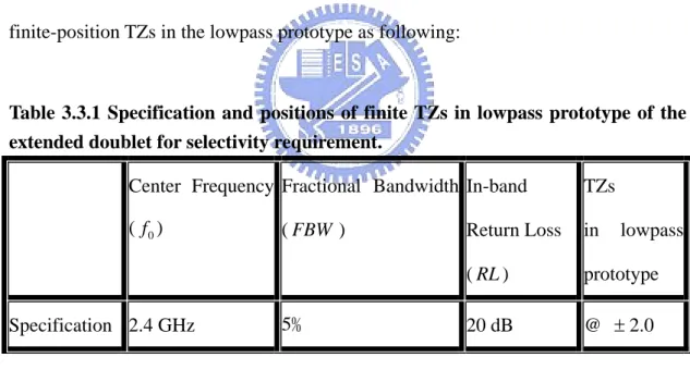
After numerical synthesis, we have the coupling matrix M with specification and finite-position TZs in the lowpass prototype as following:
Table 3.3.1 Specification and positions of finite TZs in lowpass prototype of the extended doublet for selectivity requirement.
Center Frequency ( f ) 0 Fractional Bandwidth (FBW ) In-band Return Loss (RL ) TZs in lowpass prototype Specification 2.4 GHz 5﹪ 20 dB @ ± 2.0
Table 3.3.2 Coupling matrix of the extended doublet for selectivity requirement.
S 1 2 3 L
S 0.8613 0.6202
1 0.8613 -0.8613
3 1.3878
L -0.8613 0.6202
As expressed in 3.2, we utilize those derived formulae for realizing the doublet section first. After letting the 5th row and column blank, which corresponds to the doublet section as we attempt to design right now, we find that the frequency response of the S parameters is like a notch filter in the center frequency. With the commercial simulation solver Advanced Design System (ADS) of the Agilent Inc., we have the circuit, layout, and frequency response shown in Figure 3.3.1 and Figure 3.3.2.
Figure 3.3.1 Circuit and layout of the doublet for selectivity requirement.
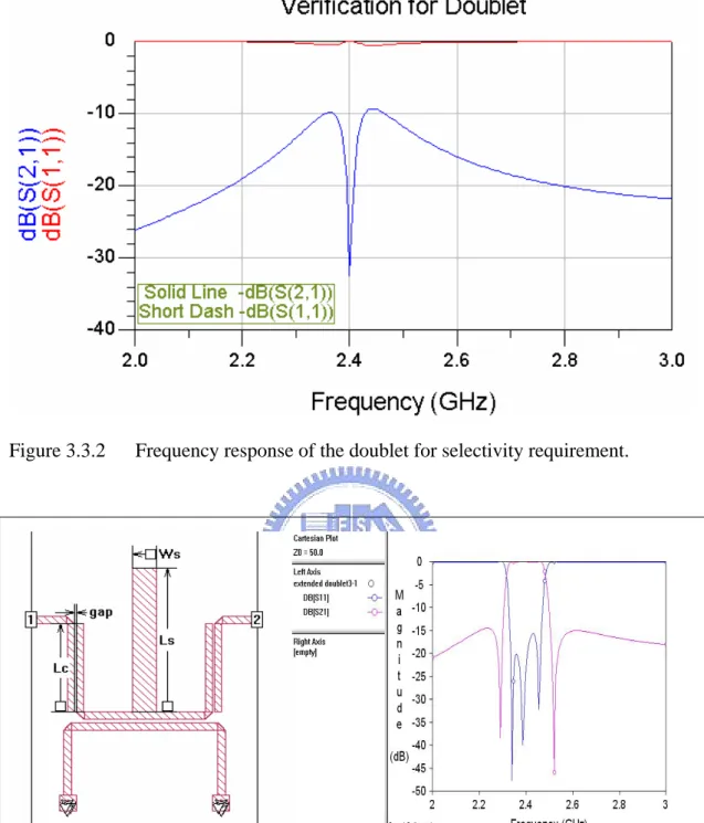
Following, attach the 3rd resonator to the aforementioned circuit and simulate the complete structure in the EM software Sonnet of Sonnet Inc. After fine tune, the physical dimensions of the extended doublet for selectivity requirement are acquired. Figure 3.3.3 indicates the final layout and simulation results under lossless condition.
Figure 3.3.2 Frequency response of the doublet for selectivity requirement.
Figure 3.3.3 The final layout and simulation results (under lossless condition) of the extended doublet for selectivity requirement. Dimension (in mils) Lc=278, gap=7, Ls=454, Ws=71.
Figure 3.3.4 illustrates the photograph of the device. The entire circuit was manufactured on a Rogers RO6010 substrate with εr=10.2 and thickness of 25 mil. Both numerical and experimental results of the frequency responses of the extended
doublet for selectivity requirement are shown in Figure 3.3.5.
Figure 3.3.4 The photograph of the extended doublet for selectivity requirement.
Extended Doublet for Selectivity Requirement
Frequency (GHz) 2.0 2.2 2.4 2.6 2.8 3.0 R e tu rn/ T ra ns m is s io n L o s s (d B ) -40 -30 -20 -10 0 Simulation result-|S11| Simulation result-|S21| Measured result-|S11| Measured result-|S21|
Figure 3.3.5 Measured and simulated S parameters of the extended doublet for selectivity requirement.
3.3.2 The Extended Doublet for Flat-Group-Delay Requirement
After numerical synthesis, we have the coupling matrix M with specification and finite-position TZs in the lowpass prototype as following:
Table 3.3.3 Specification and positions of finite TZs in lowpass prototype of the extended doublet for flat-group-delay requirement.
Center Frequency ( f ) 0 Fractional Bandwidth (FBW ) In-band Return Loss (RL ) TZs in lowpass prototype Specification 2.4 GHz 5﹪ 20 dB @ 3.0± j
Table 3.3.4 Coupling matrix of the extended doublet for flat-group-delay requirement. S 1 2 3 L S 0.7347 0.8190 1 0.7347 -0.7347 2 0.8190 1.4781 0.8190 3 1.4781 L -0.7347 0.8190 Proposed structure 1
In this configuration, we use the structure proposed in last section with some modification. Follow the same design procedure as in the case of requirement for selectivity, the extended doublet for flat-group-delay requirement is realized with ease.
Figure 3.3.6 indicates the layout and simulation results under lossless condition.
Figure 3.3.6 The layout and simulation results (under lossless condition) of the 1st proposed extended doublet for flat-group-delay requirement. Dimension (in mils) Lc=455, gap=6, Ls=288, Ws=71.
Figure 3.3.7 illustrates the photograph of the device. The entire circuit was manufactured on substrate with εr=10.2 and of thickness 25 mil. Both numerical and experimental results of the frequency responses of the extended doublet for flat-group-delay requirement are shown in Figures 3.3.8 and 3.3.9.
Figure 3.3.7 The photograph of the 1st proposed extended doublet for flat-group-delay requirement.
Extended Doublet for Flat_Group_Delay Requirem ent Frequency (GHz) 2.0 2.2 2.4 2.6 2.8 3.0 R e tu rn / In s e rt io n L o s s (d B ) -40 -30 -20 -10 0
Sim ulation result-|S11| Sim ulation result-|S21| M easured result-|S11| M easured result-|S21|
Figure 3.3.8 Measured and simulated S parameters of the 1st proposed extended doublet for flat-group-delay requirement.
Extended Doublet for Flat_Group_Delay Requirement Group Delay Response
Frequency (GHz) 2.0 2.2 2.4 2.6 2.8 3.0 G rou p D e la y (n s ) 0 5 10 15 20 Simulation result Measured result
Figure 3.3.9 Measured and simulated group delay of the 1st proposed extended doublet for flat-group-delay requirement.
As shown in the graphs, they are in good agreement. But this configuration utilized for implementing the flat-group-delay requirement has the inherent limitation of the performance on the linear phase response due to its natural property of the relative magnitude limitation in external quality factors of the odd/even modes.
Therefore, we propose the 2nd structure:
Proposed structure 2
Figure 3.3.10 shows the layout and simulation results under lossless condition.
Figure 3.3.10 The layout and simulation results (under lossless condition) of the 2nd proposed extended doublet for flat-group-delay requirement. Dimension (in mils) gap_1=3, gap_2=5.
Figure 3.3.11 The photograph of the 2nd proposed extended doublet for flat-group-delay requirement.
Figure 3.3.11 illustrates the photograph of the device. The entire circuit was manufactured on substrate with εr=10.2 and of thickness 25 mil. Both numerical and experimental results of the frequency responses of the extended doublet for flat-group-delay requirement are shown in Figures 3.3.12 and 3.3.13.
Extended Doublet for Flat_Group_Delay Requirem ent (Modified Version) Frequency (GHz) 2.0 2.2 2.4 2.6 2.8 3.0 R et u rn / I n ser ti on L o ss( dB ) -60 -50 -40 -30 -20 -10 0 Simulation result-|S11| Simulation result-|S21| Measured result-|S11| Measured result-|S21| Simulation result
without loss included-|S11| Simulation result
without loss included-|S21|
Figure 3.3.12 Measured and simulated S parameters of the 2nd proposed extended doublet for flat-group-delay requirement.
E x t e n d e d D o u b l e t f o r F l a t _ G r o u p _ D e l a y R e q u i r e m e n t ( M o d i f i e d V e r s i o n ) G r o u p D e l a y R e s p o n s e F r e q u e n c y ( G H z ) 2 . 0 2 . 2 2 . 4 2 . 6 2 . 8 3 . 0 G rou p D e la y (n s) 0 5 1 0 1 5 2 0 S i m u l a t i o n r e s u l t S i m u l a t i o n r e s u l t w i t h o u t l o s s i n c l u d e d M e a s u r e d r e s u l t
Figure 3.3.13 Measured and simulated group delay of the 2nd proposed extended doublet for flat-group-delay requirement.
As shown in Figure 3.3.13, the new proposed configuration exhibits good in-band group delay as desired. The variation of the group-delay in the passband is less than 0.5 ns in the measurement. Figure 3.3.14 shows the measured data. Furthermore, as an excellent improvement for flat group delay requirement, the 2nd proposed structure doesn’t exist the unwanted cross-coupling between resonators 1 and 2, which has been found to severely degrade the in-band linear phase response in paper [7].
Extended Doublet for Flat_Group_Delay Requirement (Modified Version) Frequency (GHz) 2.0 2.2 2.4 2.6 2.8 3.0 Re tu rn/ I n s e rt io n L o s s (d B) -30 -25 -20 -15 -10 -5 0 Gr ou p De la y (n s ) 0 5 10 15 20 Measured result-|S11| Measured result-|S21|
Measured result-Group Delay
Figure 3.3.14 The measured data of the 2nd proposed extended doublet for flat-group-delay requirement.
Chapter 4 Third-Order Transversal Filter
4.1 Introduction of the 3
rd-Order Transversal Filter
Second-order transversal filters (i.e., doublet) are the simplest building blocks for generating the finite-position TZ. In paper [11], authors have used this coupling scheme for implementing the finite-position TZ, but the T-shaped resonator was not modeled as a dual-mode resonator. Instead, the circuit was modeled as two quarter-wavelength resonators with a tapped open stub in the center plane. The open stub is considered both as a K-inverter between two quarter-wavelength resonators to control the coupling strength and as a quarter-wave open stub to generate transmission zero at desired frequency. A 3rd–order transversal filter is synthesized in [12], but not yet developed any analytical approach to systematically design the transversal filters.
In this chapter, we will establish one algorithm contributing to the fast realization of the 3rd-order transversal filter and successfully verify the possibility of such method from the simulation solver and experiment results. Figure 4.1.1 describes the routing and coupling scheme of the 3rd-order transversal filter.
As an aid for circuit tuning and investigation of the feasibility of the proposed structure, sensitivity analysis has been incorporated in the design procedure and that issue has attracted some researchers to pay attention to [13], [14]. Sensitivity determination is an important step regarding the manufacturing tolerance. From these sensitivities, acceptable bounds on the errors in the entries of the coupling matrix can be determined before an attempt is made to implement the network. Based on these results, the actual implementation can be either pursued or abandoned.
4.2 Introduction of an Analytical Approach for Synthesis
Based on the Chosen Layout
After given the specification and determining the filter order, coupling routine, and positions of finite-position TZs, we have to choose the suitable filter structure for implementation. For the 3rd-order transversal filter, we take advantage of the configuration proposed in [12] with the even- and odd-mode analysis to accelerate the synthesis of this filter. The structure is shown in Figure 4.2.1.
If a network is symmetrical, it is convenient for network analysis to bisect the symmetrical network into two identical halves with respect to its symmetrical interface. In this stage, the design procedure for the 3rd-order transversal filter based on the even- and odd-mode analysis is ready to be addressed in detail.
Assuming that the resonant frequency of the odd-mode is at f , and the 1
individual resonant frequencies of the even-modes are at f , for upper stub, 2 f for 3
lower stub, respectively. Please refer to Figure 4.2.2 and Figure 4.2.3 for structures and notations in discussion.
Figure 4.2.1 The 3rd-order transversal filter with even- and odd-mode analysis.
Step 1.
Given the coupling matrix M in the low-pass prototype, center frequency f and 0
fractional bandwidth FBW . Step 2. At 11 1 0 1 2 M FBW f = f ⎛⎜ − • ⎞⎟ ⎝ ⎠ (4.1) Specify θc. Step 3. Calculate
1 1 0 2 S S J FBW M Y π • = (4.2) with 2 1 1 0 0 0 2 2 0 1 0 1 csc 1 cot S S c e S c J J Y Y Z Z J Y θ θ ⎛ ⎞ ⎛ ⎞ +⎜ ⎟ +⎜ ⎟ ⎝ ⎠ ⎝ ⎠ = ⎛ ⎞ − ⎜⎝ ⎟⎠ (4.3) 2 1 1 0 0 0 2 2 0 1 0 1 csc 1 cot S S c o S c J J Y Y Z Z J Y θ θ ⎛ ⎞ ⎛ ⎞ −⎜ ⎟ +⎜ ⎟ ⎝ ⎠ ⎝ ⎠ = ⎛ ⎞ − ⎜⎝ ⎟⎠ (4.4)
for the values of Z and 0e Z . 0o
Step 4. Then 2 u c π θ = − (4.5) θ
Figure 4.2.2 Configuration under odd-mode analysis for the 3rd-order transversal filter. Step 5. At 22 2 0 1 2 M FBW f = f ⎛⎜ − • ⎞⎟ ⎝ ⎠ (4.6) Find out 2 0 S J Y 2 2 2 0 0 0 S S J J a b c Y Y ⎛ ⎞ + ⎛ ⎞+ = ⎜ ⎟ ⎜ ⎟ ⎝ ⎠ ⎝ ⎠ (4.7)
with 2 ' 0 0 1 e cot c Z a Z θ = + ' csc c b= θ (4.8) 0 0 1 Z e c Z = − where ' 2 1 c c f f θ =θ • (4.9)
Figure 4.2.3 Configuration under even-mode analysis for the 3rd-order transversal filter.
Step 6.
Define the impedance ratio r
3 2 Z r Z = (4.10) Calculate θ02 (initially assume the impedance ratio r = ) 1
(
)
2 2 2 03 03 02 02 2 01 2 03 01 0 2 02 sec sec 2 1 tan sin 2 tan S S J r Y M FBW r θ θ θ θ θ θ θ θ ⎡ ⎤ + ⎛ ⎞ ⎢ ⎥ = − ⎜ ⎟ • ⎢ ⎝ ⎠ • ⎥ + ⎣ ⎦ (4.11) where 2 01 1 2 f f π θ = (4.12) 2 03 01 3 f f θ = •π −θ (4.13) and 33 3 0 1 2 M FBW f = f ⎛⎜ − • ⎞⎟ ⎝ ⎠ (4.14) Step 7. At 33 3 0 1 2 M FBW f = f ⎛⎜ − • ⎞⎟ ⎝ ⎠ Find out 3 0 S J Y 2 3 3 0 0 0 S S J J a b c Y Y ⎛ ⎞ ⎛ ⎞ ′⎜ ⎟ + ′⎜ ⎟+ =′ ⎝ ⎠ ⎝ ⎠ (4.15) with 2 ' 0 0 1 e cot c Z a Z θ ′ = + ' csc c b′ = θ (4.16) 0 0 1 Z e c Z ′ = − where ' 3 1 c c f f θ =θ • (4.17) Step 8.Calculate θ03 (initially assume the impedance ratio r= ) 1
(
)
2 2 2 02 02 03 03 3 01 2 02 03 01 0 3 sec sec 2 1tan tan sin 2
S S r J r Y M FBW θ θ θ θ θ θ θ θ ⎡ ⎛ ⎞ ⎤ • + = ⎢ ⎥ − ⎜ ⎟ • + • ⎢⎣ ⎝ ⎠ • ⎥⎦ (4.18)