國
立
交
通
大
學
電子工程學系 電子研究所碩士班
碩
士
論
文
考量差動訊號及壓降避免之球閘陣列封裝針腳排列
與基板繞線
Pin Assignment and Substrate Routing on BGA Package
Considering Differential Pairs and IR Drop
研 究 生:楊尊宇
指導教授:陳宏明 博士
考量差動訊號及壓降避免之球閘陣列封裝針腳排列
與基板繞線
Pin Assignment and Substrate Routing on BGA Package
Considering Differential Pairs and IR Drop
研 究 生:楊尊宇 Student:Tsun-Yu Yang
指導教授:陳宏明 博士 Advisor:Dr. Hung-Ming Chen
國 立 交 通 大 學
電子工程學系 電子研究所碩士班
碩 士 論 文
A Thesis
Submitted to Department of Electronics Engineering & Institute of Electronics College of Electrical and Computer Engineering
National Chiao Tung University in partial Fulfillment of the Requirements
for the Degree of Master
in
Electronics Engineering September 2009
考量差動訊號及壓降避免之球閘陣列封裝針腳排列
與基板繞線
研究生:楊尊宇 指導教授:陳宏明 博士 國立交通大學 電子工程學系 電子研究所 碩士班摘 要
隨著現今超大型積體電路縮小至深次微米技術,使得晶片設計、封裝與印
刷電路板的複雜化急遽增加,造成晶片、封裝跟印刷電路板界面間之設計變得
更加費時,因此晶片封裝協同設計便成為關鍵且必要的工作。晶片封裝協同設
計分成兩個階段,第一個階段為針腳配置,另一個則為基板繞線。針腳配置階
段主要是決定訊號在晶片接點銲墊(I/O pad)、銲線(finger)、金屬球凸塊(bump ball)
的位置。另一方面,基板繞線則是在封裝基底上將銲線跟對應的金屬球凸塊訊
號連接起來。本篇論文針對晶片與封裝之協同設計而提出一個考量差動訊號及
壓降避免的針腳指定演算法,並利用修改 A*演算法之價值函數來實現基板繞線
以增加可繞度及減少繞線層數。實驗結果顯示:在合理的封裝尺寸之下,本篇
論文所提出的針腳指定及基板繞線演算法可以有效減少所需繞線層數。
關鍵字:球閘陣列封裝、針腳指定、基板繞線、電阻壓降、差動訊號、晶片封裝協同設計Pin Assignment and Substrate Routing on BGA Package Considering
Differential Pairs and IR Drop
Student: Tsun-Yu Yang Advisor: Dr. Hung-Ming Chen
Department of Electronics Engineering Institute of Electronics
National Chiao Tung University
ABSTRACT
While the advanced very large scale integration (VLSI) circuit is scaling to deep-submicrometer (DSM) technology, the complication in designing chips, packages and the communications between package and board become increasingly significant. The iterative interface design between chip, package and board has been a time-consuming process. As a result, a chip-package-board co-design flow is critical and necessary. The co-design flow contains two stages: one is pin assignment and the other is package substrate routing. The pin assignment is to determine the location of I/O signals, fingers and bump balls on ball gird array (BGA) packages. On the other hand, the package substrate routing is to connect each finger with its corresponding bump ball by wire segments. In this thesis, we have proposed a new pin assignment algorithm for the chip-package-board co-design flow considering the differential pair signals and IR-drop. We also have applied a modified A* algorithm to implement the substrate routing which increases the routability and reduces the total number of layers. The experimental results show that our methodologies can effectively reduce the number of layers while controlling package size to be a reasonable one.
誌 謝
終於結束了口試,要離開這個帶給我許多回憶的地方了,兩年一下子就過去了,轉眼間 我也即將邁入社會,脫離學生的生活。 首先,我要感謝我的家人,他們提供了我相當優渥的環境,可以在這個學校裡面充實我 的知識,不停的學習以及成長,在我心情低落的時期可以提供我心靈上的慰藉,如果沒有我 的家人,就不會有今天的楊尊宇,謝謝。 回想兩年多前剛進入陳宏明老師的歡樂 VDA 實驗室,焦頭爛額地修課寫做專題,到後來 參予 IC/CAD Contest 開始了我的研究題目,構思自己的演算法,到最後的口試,整理論文, VDA 實驗室裡面的許多學長和同學們給予了我相當多的幫助,讓我可以順利畢業。陳宏明老 師給予我們充分的自由與發展空間,包容我們,鼓勵我們,謝謝老師。 從小碩一開始,我就跟著李仁傑學長學習相關的知識,他對我的照顧以及幫助,我真的 有千言萬語也訴說不盡,真的非常謝謝你。同時,也謝謝我的夥伴們,Bug、便便、宅叡、小 胖、阿鬍還有娘扣,以及各位學長姐們,一直以來一直陪著我經歷這些風風雨雨,讓我可以 順利的畢業,非常感激你們。 最後要特別感謝我的男朋友,施經緯,在我寫論文苦悶的時候給我加油打氣,讓我可以 提起精神繼續振作。 要感謝的人太多了,陪我度過這段時間的各位們,我愛你們! P .S. 小舅,我順利從交大電子所拿到畢業證書了!Contents
中文摘要 ... i Abstract ... ii 誌謝 ... iii Contents ... iv List of Figures ... viList of Tables ... viii
Chapter 1 Introduction... 1
1.1 Package Design Flow... 2
1.2 Previous Works ... 4
1.3 Thesis Organization ... 5
Chapter 2 Preliminaries ... 6
2.1 Package Design Overview ... 6
2.2 Problem Description ... 8
2.3 Signal Type Definition and Characteristic ... 9
2.4 BGA Ball Ordering Scheme... 10
2.4.1 Definitions of BGA Ball Ordering Scheme ...11
Chapter 3 Methodology ... 14
3.1 Pin Assignment ... 14
3.1.1 Ball Assignment ... 16
3.1.2 Finger Assignment ... 21
3.2 Substrate Routing... 25
3.3 Routability Checking ... 29
Chapter 4 Experimental Results... 31
Chapter 5 Conclusions... 34
List of Figures
1.1 An illustration of PCB and BGA. ... 1
1.2 The side view of BGA package... 2
1.3 Traditional Package Design Flow. The packaging stage is on the bottom of the design flow and the locations of fingers and bump balls are determined at the physical design stage. ... 3
2.1 The Chip-Package-Board Co-design Flow. The Pin assignment considers chip, package and board information to determine pin locations. ... 6
2.2 An Illustration of BGA Region. BGA board is separated into four regions: N,E,W, and S. And the board is also separated into middle and corner regions; we prefer to assign signals to middle region instead of corner regions. ...11
2.3 The monotonic order of a BGA system. While routing in this order, the routability can become maximum. ... 12
3.1 Pin Assignment Flow. In the beginning, bump balls are assigned; and we assign corresponding fingers in monotonic order. While assigning balls, according to the importance of signal types, we first assign power/ ground signals; then, PCB signals which have to connect to PCB components are assigned; Finally, we assign BGA signals which just connect to BGA bump balls instead of PCB components. ... 15
3.2 Power Assignment Flow... 16
3.3 PCB Assignment Flow... 17
3.4 BGA Assignment Flow. ... 19
3.6 Finger Region Refinement Algorithm ... 24 3.7 Routing Order Determination ... 26 3.8 The EvaluateCost function of different routing stages. ... 29
List of Tables
4.1 Detailed information of the test cases [12]. ... 31 4.2 Experimental Results Compared with Cadb004 [12]. ... 32 4.3 Experimental Results Compared with NTHU [13] ... 32
Chapter 1
Introduction
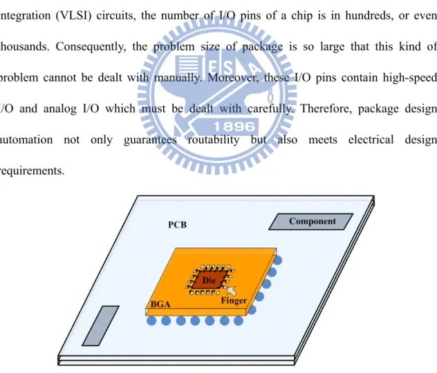
In the past, the I/O number on a package is usually less than one hundred, and therefore this kind of problem is usually achieved manually. However, with the shrinking of the technology, the functionality of one chip becomes more and more complicated such that the I/O number of a chip increases. In current very large scale integration (VLSI) circuits, the number of I/O pins of a chip is in hundreds, or even thousands. Consequently, the problem size of package is so large that this kind of problem cannot be dealt with manually. Moreover, these I/O pins contain high-speed I/O and analog I/O which must be dealt with carefully. Therefore, package design automation not only guarantees routability but also meets electrical design requirements.
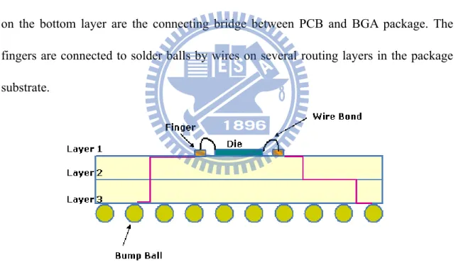
Nowadays, ball grid array (BGA) is used to realize the large number of connections between VLSI chips and Printed Circuit Boards (PCB). As Figure 1.1 shows, PCB is a board which contains components and BGA package(s) on it and acts as a connecting bridge from one signal to another by routing nets. On the other hand, wire bonding or flip-chip techniques are chosen to connect a die to the substrate. In this thesis, wire bonding is chosen. Figure 1.2 is the side view of BGA package, and this illustrates a wire bonding and BGA package model. In a BGA package, pads on a chip are connected to bonding fingers on the top layer of package substrate. The solder balls on the bottom layer are the connecting bridge between PCB and BGA package. The fingers are connected to solder balls by wires on several routing layers in the package substrate.
Figure 1.2: The side view of BGA package.
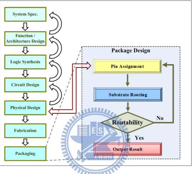
1.1 Package Design Flow
In current design methodology, package design is on the bottom of the whole VLSI design flow as Figure 1.3 shows. The package design is mainly divided into two stages:
Figure 1.3: Traditional Package Design Flow. The packaging stage is on the bottom of the design flow and the locations of fingers and bump balls are determined at the physical design stage.
z Pin assignment:
According to the input of chips, components and different signals types, the purpose of pin assignment is to optimize pin locations. The key point on package design is to shrink the package size. For this objective, we should do the pin assignment optimization in order to reduce the number of needed layers of routing, total length of routing and via numbers.
z Substrate Routing:
The purpose of substrate routing is to connect signals from a chip inside to outside components. When doing substrate routing, there are several design rules which must be met: one is the routing segments (on the same layer) should not overlap and cross. Another is the minimum space between wires or between a wire and a bump ball. The final one is the minimum wire width.
Traditionally, pin location is assigned by chip designer. Then package and PCB designers follow the chip’s pin assignment to determine the package size and the number of routing layers. But without components information, the pin assignment cannot be optimized, which might waste plenty of routing space and increase the difficulties during routing. Therefore, pin assignment optimization becomes the main issue in package design.
1.2 Previous Works
To the best of our knowledge, there is no research for pin assignment problem in package design. But there are some works in substrate routing. The package routing problem can be divided into two kinds. One is the free-assignment problem and the other is the pre-assignment problem. Free-assignment determines pin locations during routing process, which can be easily implemented by using network flow formulation [1] [2] [3]. On the other hand, pre-assignment determines fingers and ball locations before routing. This kind of problem is much harder than free-assignment, because the signal
mapping from fingers to bump balls have been fixed and cannot be changed in the routing procedure. Moreover, the pre-assignment problem is more practical since the functions of fingers and balls are typically predefined by chip and package designers.
Under the scenario that which bump ball is going to be connected to a finger is pre-assigned, the works [4] [5] [6] proposed routing algorithms for multi-layer BGA and Pin Grid Array (PGA) package. The works [7] [8] proposed routing algorithms for 2-layer BGA package and these works are applied to a given BGA package and the connection relations between fingers and bump balls are pre-assigned.
In this thesis, we propose a new pin assignment algorithm for chip-package-board co-design flow and combine pin assignment and package substrate routing to implement a package design. More than that, we also consider differential pair signal and IR drop constraints in this thesis.
1.3 Thesis Organization
The rest of this thesis is organized as follows. Chapter 2 introduces the background of package design automation flow, the problem description, types of signals and the BGA ball ordering scheme. Chapter 3 describes the methodology of pin assignment and substrate routing. Chapter 4 shows the experimental results and followed by the conclusion and the future work in Chapter 6.
Chapter 2
Preliminaries
In this chapter, we first introduce the overview of package design flow in Section 2.1. Second, in Section 2.2, we describe the problem of the package design. Then the definitions of signal types are shown in Section 2.3. Finally, in Section 2.4, the BGA ball ordering scheme of this thesis for pin assignment and substrate routing is introduced.
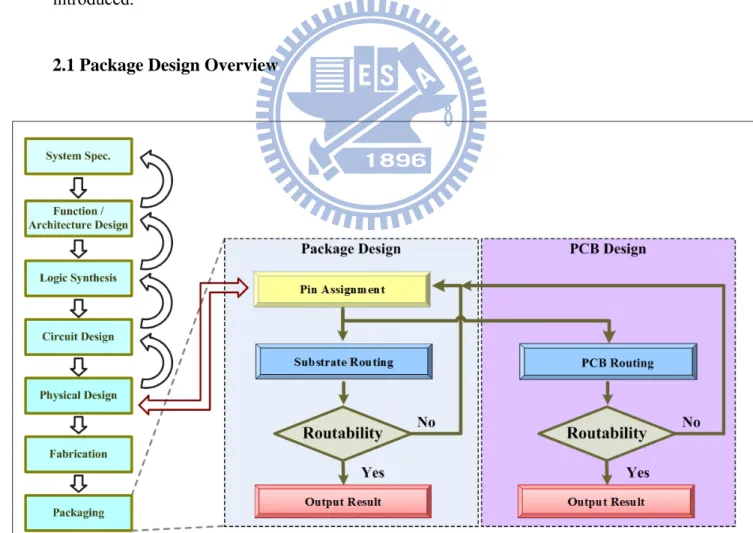
2.1 Package Design Overview
Figure 2.1: The Chip-Package-Board Co-design Flow. The Pin assignment considers chip, package and board information to determine pin locations.
In the traditional design flow, physical design stage determines the locations of I/O pads and fingers, and then generates a GDSII of one chip. According the given locations of I/O pads, packaging stage finishes substrate routing. However, if the routability of substrate routing is not 100%, the flow has to return to physical design to modify the locations of I/O pads and fingers, then do package synthesis and package design again and again until routability reaches 100%. This sequential flow is time-consuming that the chip design, the package design, and the PCB design have to be considered at the same time.
For the reason mentioned above, a concurrent design flow is proposed [9]. As Figure 2.1 shows, when at physical stage, the pin assignment arranges locations of I/O pads and fingers according to the chip information, package information, and PCB information. In other words, pin assignment considers chip design, package design, and PCB design at the same time to optimize these locations. When finishing pin assignment, chip design, package design, and PCB design can start their work concurrently. If any part of design fails, we return to pin assignment stage and adjust the pin locations. According to the modified result, the designers of chip, package, and PCB then start to modify their design concurrently. Therefore, this concurrent design flow will reduce time to market.
In this thesis, we just focus on package design. The main idea is to propose one pin assignment algorithm with the co-design consideration and combine this pin assignment and substrate routing for developing a package design flow. To simplify this problem,
the chip information is not considered in this thesis. This problem just gives us the locations of fingers, the locations of component pins, and the netlist of signals to deal with.
2.2 Problem Description
Because the pin sequences of each component are fixed on a PCB but not on an ASIC chip, we can take the optimization of routing resource as the objective to decide the pin locations on an ASIC chip and to reduce the routing between an ASIC chip and PCB components with the consideration of the relation between an ASIC chip and PCB component signals. In other words, the problem to solve is considering both the routing on an ASIC chip and the routing between an ASIC chip and a PCB component. We specify inputs, outputs and goals of this problem which are shown below:
Problem inputs:
1. The locations of components, component pins, and ASIC fingers.
2. The electrical interconnections are described in a netlist, which contains differential pair signals and power signals constraints.
3. Design rules of BGA package.
Problem outputs:
2. Routing wires connecting fingers to bump balls in BGA package. The routing segments include vertical and horizontal wire segments and vias.
Problem goals:
While meeting all design rules (especially differential pair signal and power signal constraints), we obtain optimized pin assignments from pins in PCB components to BGA package bump balls and from BGA package bump balls to fingers with objective of minimizing the package size, the number of total routing layers and total wire length.
2.3 Signal Type Definition and Characteristic
In this thesis, differential pair signals and power/ ground signals are considered due to their importance. There are three types of signals, and the following will describe their definitions and characteristics:
1. Power/ Ground signals:
This is steady and in charge of supporting power for a working chip in the whole system.
2. General purpose signals:
This is a general purpose I/O of a chip which is used for low speed or long-pause signals.
3. Differential pair signals:
Differential pair is a pair of conductors with special characteristics, used for differential signaling. These pairs are generally used to carry high-speed digital serial interfaces, or used for high quality and/or high frequency analog signals, etc. This kind signal is also an I/O of a chip but must appear in pairs, and should be near by each other no matter in assigning or in routing stages.
Moreover, the second and the third types of signals are classified into 2 kinds: a signal which just connects to a bump ball, and a signal which connects to not only a bump ball but also a component pin.
2.4 BGA Ball Ordering Scheme
The BGA board scheme of this thesis is shown in Figure 2.2. The circles, which are as the base of the BGA system, are bump balls in the bottom of the whole BGA package. The BGA package is divided into 4 regions: east(E), south(S), west(W) and north(N) for simplifying the problem when routing. Separating region can make the routing nets shorter, increase the routability, and limit searching space. And the BGA package is also separated into corner and middle regions, and we prefer to assign signals to middle regions in order to avoid routing to corner region because balls in the corner region will cause the bottleneck while routing. Next, on the top of the package, which is the rectangle in the middle of Figure 2.2, is a chip. Then, between the chip and the bump balls, there are several layers, on which the routing nets must not overlap with each
other.
Figure 2.2: An Illustration of BGA Region. BGA board is separated into four regions: N,E,W, and S. And the board is also separated into middle and corner regions; we prefer to assign signals to middle region instead of corner regions.
2.4.1 Definitions of BGA Ball Ordering Scheme
Definition 1: Track number
Track number means the maximum number of nets that can pass through between two adjacent balls without violating design rules.
Definition 2: Nring(n)
Nring(n) represents that the ball n is on which number of ring of the BGA package.
The number of ring in the most inner ring is 1, and the number of ring from the most inner to the most outer is in increasing order one after another, as shown in Figure 2.2.
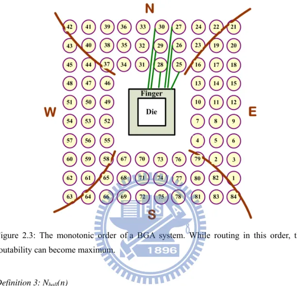
Figure 2.3: The monotonic order of a BGA system. While routing in this order, the routability can become maximum.
Definition 3: Nball(n)
In this thesis, each bump ball n has its own index, Nball(n), which represents the monotonic routing order on BGA.
Definition 4: Monotonic order
For avoiding crosses and maximizing the routability on the routing plane, we define the routing order of bump balls. The order is shown in Figure 2.3.
Definition 5: Routing cost
(2.1) ⎩ ⎨ ⎧ = otherwise. , via. a is candidate when constant Cost α β,
Definition 6: Distance function ) ( _ ) ( _ ) ( _ ) ( _ ) ( _ ) ( _ b coordinate Z a coordinate Z b coordinate Y a coordinate Y b coordinate X a coordinate X b) , Distance(a − × + − × + − × = β α α (2.2)
Chapter 3
Methodology
In this chapter, we introduce detailed pin assignment algorithm and substrate routing algorithm in Section 3.1 and Section 3.2. Finally, the routability checking procedure is presented in Section 3.3.
As soon as finish inputting one test case, classifying and analyzing the data for test case should be done. This will let the data be used efficiently when beginning our algorithm.
1. Compute the number of inner and outer fingers in each side.
2. Give initial track number and layer number to determine the BGA package size.
3. Construct BGA package data structure and set Nring(n), Nball(n).
4. Sort components in order.
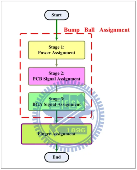
3.1 Pin Assignment
The goal for pin assignment is to assign the positions of fingers and bump balls. The procedure is shown in Figure 3.1. At first, we arrange the signal on the bump balls according to component pin location and the importance of each kind signal. After
ensuring bump ball location of each signal, we assign the corresponding finger according to monotonic order.
Figure 3.1: Pin Assignment Flow. In the beginning, bump balls are assigned; and we assign corresponding fingers in monotonic order. While assigning balls, according to the importance of signal types, we first assign power/ ground signals; then, PCB signals which have to connect to PCB components are assigned; Finally, we assign BGA signals which just connect to BGA bump balls instead of PCB components.
3.1.1 Ball Assignment
According to the importance of signal type, there are three stages in ball assignment: First, in order to avoid IR drop, let power/ground signal pairs average spread on BGA package. Second, arrange PCB signals to outer rings on BGA package. This will put them close to their belonged component pins. Finally, assign BGA signals to inner ring on BGA package to reduce wirelength of substrate routing.
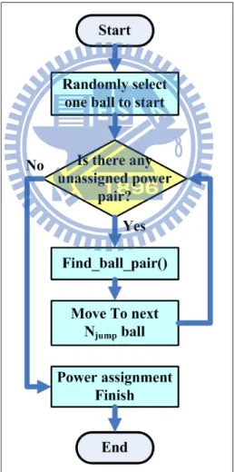
Step 1: Power Assignment
The objective of this step is to let power supply pins be averagely distributed on BGA array. As Figure 3.2 shows, in the beginning, randomly choose one ball to assign. Then assign other power pair signals every other Njump balls.
Step 2: PCB Signal Assignment
In package design, PCB signals need to connect to bump balls of BGA package and to outside components; on the other hand, BGA signals just have to connect to bump balls. Therefore, if allocating PCB signals to outer rings of BGA package and BGA signals to inner rings, the total wirelength of package and PCB routing will be reduced.
The flow of PCB assignment is shown in Figure 3.3. First, select the region of first order component to start. Second, if current signal is differential pair signal, apply Find_ball_pair function to get ball pair and then assign the signal pair at the same time. Otherwise, if it is not, apply Find_ball function to find an empty ball for allocating current signal. In the end, if the whole PCB signals are arranged, the procedure of PCB assignment is done.
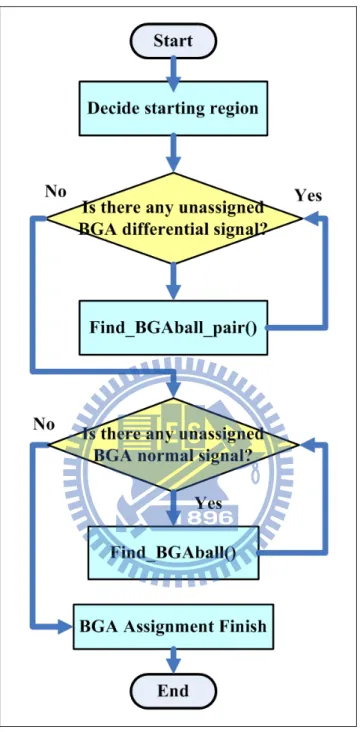
Step 3: BGA Signal Assignment
Because differential pair signals have to put next to each other and route next to each other, this will separate the routing region and increase the routing difficulty. Therefore, differential pair signals will be allocated at inner rings. And then normal BGA signals will fill other empty bump balls. But when assigning, corner region of BGA package will be the last choice to be allocated. This is because corner region will be the most crowded region while routing.
Figure 3.4: BGA Assignment Flow.
As Figure 3.4 shows, first choose the sparsest region to start BGA assignment. Second, assign BGA differential pair signals first. Find empty pair balls with Find_BGAball_pair function. After BGA differential pair signals are all assigned, start
to assign BGA normal signals. Apply Find_BGAball function to assign normal signal one by one until all signals have their own bump ball locations.
Detailed Function Description:
1. Begin with start point, find an empty ball in monotonic order to assign a signal ( Find_ball( ) ).
In this function, set the n-th ball, which means Nball is n, to be starting ball. If this ball is not be assigned yet, which means the ball is free, then the n-th ball is selected to assign a signal. Otherwise, if it is not free, then put off to the n+1-th ball and so on. If all the balls can't be free to be selected, this function fails.
2. Begin with start point, find an empty ball in monotonic order to assign a signal pair ( Find_ball_pair() ).
In this function, set the n-th ball, which means Nball is n, to be starting ball. If this ball and the ball next to it are not be assigned yet, then this ball pair are selected to assign a signal pair. Otherwise, if they are not free, then put off to the n+1-th ball and so on. If all the balls can't be free to be selected, this function fails.
3. Begin with start point, find an empty ball from inner ring to outer ring to assign a signal ( Find_BGAball() ).
In this function, set the starting ball to be Sp. If this ball is not be assigned yet, which means the ball is free, then it is selected to assign a BGA signal. Otherwise, if it is not free, then go counterclockwise to find a free ball and assign a BGA signal until meet Sp. If meet Sp, it means there is no free ball in this ring, and then go outward to
next ring. Then set Sp to be current ball and go counterclockwise to find a free ball. If there is not free ball again, go to next ring and repeat this procedure until meet the outside boundary. If meet outside boundary, it means this function fails.
4. Begin with start point, find an empty ball from inner ring to outer ring to assign a signal pair ( Find_BGAball_pair() ).
In this function, set the starting ball to be Sp. If this ball and the ball next to it, which means the Nball is next to it, are not be assigned yet, which means the ball pair are free, then they are selected to assign a BGA signal pair. Otherwise, if they are not free, then go counterclockwise to find a free ball and assign a signal until meet Sp. If meet Sp, it means there is no free ball in this ring, and then go outward to next ring. Then set Sp to be current ball and go counterclockwise to find a free ball. If there is not free ball again, go to next ring and repeat this procedure until meet the outside boundary. If meet outside boundary, it means this function fails.
3.1.2 Finger Assignment
After finishing the ball assignment, assign the fingers in the monotonic order. The finger assignment flow is described as shown in Figure 3.5. In the beginning, we do Finger Region Assignment to collect all filled balls and separate them in belonging region. Then, because the number of filled balls in each region may not be equal to the number of fingers in corresponding region, some balls may be assigned to the finger of different region. For this reason, Finger Region Refinement assigns each different region ball to one individual finger.
Figure 3.5: Finger Assignment Flow.
Step 1: Finger Region Assignment
In this thesis, there are two kinds of fingers: one is called inner ring finger and the other is called outer ring fingers. Outer fingers can start routing nets from top layer and inner fingers have to go to second layer by vias and then start routing nets. In order to save routing resource, inner fingers tend to connect with inner balls, and outer fingers tend to connect with outer balls. Therefore, we first assign inner ring balls to inner fingers and then assign left balls to outer fingers. Note that, each region has its own inner list and outer list, and we can put selected balls in to them. The flow chart is
shown in Figure 3.5, and each region goes through the flow chart alone. The following describes the method of each stage:
At the Inner Finger Assignment stage, in order to make inner routing as easy as possible, the corner regions of BGA are not chosen in this stage. We start from most inner ring, and put each assigned ball into inner list until the number of list is equal to the number of inner fingers of this region. When current assigned ball has signal pair, put this signal pair into inner list together.
Next, at Outer Finger Assignment stage, we find all assigned balls which are not in inner list and put them into outer list of this region. Then this stage is finished.
Step 2: Finger Region Refinement
In Finger Region Assignement, the filled balls of each region are sorted in monotonic order first. Then inner list of each region assign to inner fingers in counterclockwise order. Third, because the number of outer list of each region may not match with the number of outer fingers of each region, these lists have to be adjusted. The Finger Region Refinement algorithm is shown in Figure 3.6.
First, choose the region of first order component to be the base region. The number of Remain in this region means the number of unassigned fingers of this region. If the Remain number of this region is 0, then do nothing. Or, if there are unassigned fingers/
extra balls, get/ push balls from/to two adjacent region of this region to let each finger of this region has its own signal ball.
When the finger assignment of base region is done, move to the forward region. If the Remain number of this region is 0, then do nothing. Or, if there are unassigned fingers/ extra balls, get/ push balls from/to forward adjacent region of this region to let each finger of this region has its own signal ball. When finishing this region, move to next region again, and do this procedure once. Finally, Finger Region Refinement algorithm is finished.
3.2 Substrate Routing
In this thesis, we introduce a special routing order determination and apply modified A* algorithm [10] to implement substrate routing.
3.2.1 Routing Order Determination
For routing resources are limited, routing nets order is the key point to maximize the routability of each layer. The routing order flow chart is shown in Figure 3.7. Because of the way of assigning inner balls, the balls which are assigned to inner fingers are easy to be routed counterclockwise. But the order of outer finger routing has to be dealt with carefully. In the way of separating board region, the corner region is the bottleneck during routing. Therefore, first choose the middle region balls to route. Then corner region balls and the different region balls are the last two regions to be routed.
Figure 3.7: Routing Order Determination.
Note that, in middle region, each ball is routed in increasing Manhattan distance order. Manhattan distance of this algorithm is defined in Equation 3.1.
) 1 . 3 ( ) ate(target X_corordin te(node) X_coordina ) ate(target Y_corordin te(node) Y_coordina target) ode, distance(n Manhattan_
⎩⎨
⎧
− − = S region is in N, ,when node region W is in E, ,when node3.2.2 A* Algorithm and Cost Function
The concept of A* algorithm is similar to Dijkstra algorithm [11], but A* algorithm operates the paths through constructing open list and closed list and then estimates the function by the paths to decide where to move. Finally, this algorithm finds the shortest path from source to target. This cost function finds solutions more rapidly and reduces search region in compared with Dijkstra algorithm.
Estimating function: F_Cost(candidate) = G_Cost(candidate)+ H_Cost(candidate)(3.2)
First, G_Cost(candidate) means the movement cost for moving along the generated path from initial point to the candidate location. Then H_Cost(candidate) means the movement cost for moving from candidate location to target. There are a lot of ways to find this value, and the most common one is Manhattan method, which is to calculate the moving distance between 2 points. Finally, F_Cost(candidate) is the sum of
G_Cost(candidate) and H_Cost(candidate).
z Candidate Directions
In this algorithm, moving outside is the first priority on a plane. For example, the outside direction of E region is eastern one. And in order to make the routability of plane maximum, the cost of moving downward is much bigger than other direction; i.e., let α<β. But there is one special case: because the way to assign inner fingers, inner routing can be completed in one plane. So moving downward is the first priority when
doing inner finger routing; i.e., let α>β. Moreover, note that the detour routing on a plane is allowed; but the direction between two layers can not be upward in order to save the cost of via.
z Cost Function Modification
Based on A* Algorithm Routing, we modify cost function to fit our goal. Modified cost function shows in Equation 3.3~3.4. First, Equation 3.3, which means G_Cost function of current node, computes the actual shortest distance traveled from source node to current node. Then Equation 3.4, which means H_Cost function of current node, evaluates not only the estimated distance from current node to target but also other evaluated factors which are computed in EvaluateCost Function. Finally, apply Equation 3.2 to evaluate the cost of candidate node.
G_Cost(candidate) = G_Cost(Core) + α (3.3)
H_Cost(candidate) = Distance(candidate,target) + EvaluateCost(candidate) (3.4)
EvaluateCost Function has two factors which are shown below: First Factor A is the ring number of candidate, which let the priority direction to be outward of the region; then, Factor B is the difference of Nball(candidate) and Nball(target). Figure 3.8 indicates that which factor is chosen during corresponding routing stage.
Factor A= Nring(candidate)
Factor B= | Nball(candidate) - Nball(target) | mod total_ball_number
Figure 3.8: The EvaluateCost function of different routing stages.
3.3 Routability Checking
In order to control package size in a reasonable size, Trackmax means the maximum track number. And Lmax means the maximum number of layers of this problem. If substrate routing can not achieve 100% routability, we will take following stratages: First, if current track number is less than Trackmax, then increase track number. Second,
if current track number is equal to Trackmax, then increase the number of layers until it is equal to Lmax. Finally, if the number of layers is equal to Lmax, this means the package design with our constraints can not reach 100% routability.
Chapter 4
Experimental Results
Our algorithm was implemented in C++ programming language and tested on a Linux workstation with Core 4 Intel(R) Xeon(R) E5160 3.0 GHz and 32G RAM. We used five industry cases [12] to test our algorithm. The detailed information of each case is listed in TABLE 4.1. Note that, case 1 and case 5 have the same finger set, and case 2, case 3, and case 4 have the same finger set. The PCB components of all cases, however, are not identical to each other. There are at most four routing layers we can use.
Table 4.1: Detailed information of the test cases [12].
case1 case2 case3 case4 case5 # of signals 268 429 429 429 268 # of components 1 3 4 3 1
The experimental results listed in TABLE 4.2 and TABLE 4.3 are compared with the Cadb004 [12] and NTHU [13] specifically. In these tables, the package size and the number of BGA layer are used to evaluate total package cost; on the other hand, the total wirelength on BGA can represent the performance. In our algorithm, the execution time of each case is not more than 10 seconds. And all guarantee routablilty 100%.
Table 4.2: Experimental Results Compared with Cadb004 [12].
Package Size Performance
L W Improvement BGA Layer Wirelength Improvement
Cadb004 33.6 33.6 - 2 4490 - Case1 Ours 22.76 22.76 54% 3 2518.41 44% Cadb004 47 47 - 2 10169 - Case2 Ours 28.09 28.09 64% 3 4104.64 60% Cadb004 47 47 - 2 10169 - Case3 Ours 28.09 28.09 64% 3 4160.95 59% Cadb004 47 47 - 2 10169 - Case4 Ours 28.09 28.09 64% 3 4127.33 59% Cadb004 33 33 - 2 4490 - Case5 Ours 21.54 21.54 57% 3 2227.4 50%
Table 4.3: Experimental Results Compared with NTHU [13].
Package Size Performance
L W Improvement BGA Layer Wirelength Improvement
NTHU[13] 22.6 19.32 - 4 1865.96 - Case1 Ours 22.76 22.76 -19% 3 2518.41 -35% NTHU[13] 32.05 32.05 - 4 4556.08 - Case2 Ours 28.09 28.09 23% 3 4104.64 10% NTHU[13] 32.05 32.05 - 4 4556.08 - Case3 Ours 28.09 28.09 23% 3 4160.95 9% NTHU[13] 32.05 32.05 - 4 4556.08 - Case4 Ours 28.09 28.09 23% 3 4127.33 9% NTHU[13] 22.6 19.32 - 4 1865.96 - Case5 ours 21.54 21.54 -6% 3 2227.4 -19%
First, the results are compared with Cadb004. Cadb004 is the only one team that finished the five test cases of problem B3 in the 2008 IC/CAD Contest. The method of Cadb004 is sorting all signals and surrounding the chip with the signals one by one in a ring. Finally, the method applies the simple channel routing to route the signals. Although this method must be success for routing and need only 2 layers to complete, it enlarges the package size and increases the total wirelength. The result shows: although there are one more layer be used, the package size and wirelength shrink much more than a half clearly.
Second, we compare our results with NTHU. NTHU constructed a network flow model and applied the Min-Cost-Max-Flow algorithm to solve this problem which can guarantee routability. In the case2, case3, and case4, the package size reduces 23%, the number of layers decreases one, and the wirelength reduces 9%~10%. Then in case1 and case5, we reduce the number of layers one, the package size is a little larger than NTHU, the number of layers decreases one but the wirelength increase 33% and 19% respectively. In case2, case3, and case4, because the corner region of BGA is less assigned balls, the routing flow of each signal can easily go outward direction and can avoid routing to the corner region. Therefore, the results of these three cases can get better. On the other hand, the results of case1 and case5, the bump balls on BGA are almost filled; therefore, this increases the routing difficulty and cause the package size and total wirelength increase.
Chapter 5
Conclusions
In this thesis, we propose a package design flow for the chip-package-board co-design flow. At first stage, we propose a new pin assignment algorithm considering the differential pair signals and IR-drop. With this algorithm, the whole routing space can be used more efficiently. Then at second stage, the cost function of A* algorithm and routing order effectively increases the routability and reduces the total number of layers.
The experimental results show that our methodologies improve the package size, and the total wirelength to at least 50% while increasing the number of layers by one. Then while compared with NTHU, if the corner region on BGA package is sparse, our methodologies guarantee routability and effectively reduce the number of layers, total wirelength while controling the package size in a reasonable one. Otherwise, if the corner region on BGA package is dense, the wirelength and the package size do not be improved while the number of layers still reduces to three.
In this thesis, the given information is just component pins, differential pair signals, power/ ground signals and the wire segments can just be horizontal or vertical. In the future, we want to implement one any-angle substrate routing and propose a cost function which considering the issue of the pin assignment in order to make the pin assignment more convincing.
Bibliography
[1] M.-F. Yu, J. Darnauer, and W. M. Dai, “Interchangeable Pin Routing with Application to Package Layout,” In Proceedings IEEE/ACM International Conference
on Computer-Aided Design, pages 668–673, 1996.
[2] D. Wang, P. Zhang, C.-K. Chang, and A. Sen, “A Performance-driven I/O Pin Routing Algorithm,” In Proceedings IEEE Asia and South Pacific Design Automation
Conference, pages 129–132, 1999.
[3] J.-W. Fang, I.-J. Lin, P.-H. Yuh, Y.-W. Chang, and J.-H.Wang, “A Routing Algorithm for Flip-chip Design,” In Proceedings IEEE/ACM International Conference
on Computer-Aided Design, pages 753–758, 2005.
[4] C.-C. Tsai, C.-M. Wang, and S.-J. Chen, “News: A Net-Even-Wiring System for the Routing on a multilayer PGA package,” In IEEE Transactions on Computer-Aided
Design of Integrated Circuits and Systems, vol. 17, no. 2, pages 182–189, Feb. 1998.
[5] S.-S. Chen, J.-J. Chen, S.-J. Chen, and C.-C. Tsai, “An Automatic Router for the Pin Grid Array Package,” In Proceedings IEEE Asia and South Pacific Design Automation
Conference, pages 133–136, 1999.
[6] S.-S. Chen, J.-J. Chen, C.-C. Tsai, and S.-J. Chen, “An Even Wiring Approach to the Ball Grid Array Package Routing,” In Proceedings International Conference on
Computer Design, pages 303–306, 1999.
[7] Y. Kubo and A. Takahashi, “Global Routing by Iterative Improvements for Two-Layer Ball Grid Array Packages,” In IEEE Transactions on Computer-Aided
Design of Integrated Circuits and Systems, vol. 25, no. 4, pages. 725-733, April 2006.
[8] Y.-C. Lin, K.-Y. Lee and T.-C. Wang, “A Two-Layer Global Router for Ball Grid Array Packages,” In Proceedings of The Workshop on Synthesis And System Integration
of Mixed Information technologies, pages 301–306, 2009.
[9] K. Sheth, E. Sarto, and J. McGrath, “The Importance of Adopting a Package-aware Chip Design Flow,” In Proceedings ACM/IEEE Design Automation Conference, pages 853–856, 2006.
[10] P. Lester, “A* Pathfinding for Beginners,” In GameDev.net
[11] T. H. Cormen, C. E. Leiserson, and R. L. Rivest, Introduction to Algorithms. Cambridge, MA: MIT Press, 1992.
[12] 2008 MOE/CAD Contest of Taiwan. [Online]. Available: http://cad_contest.ee.ntu.edu.tw/cad08/index.htm
[13] C.-C. Wang and T.-C. Wang, “Automatic Bump Ball Allocation/Placement and Signal Assignment/Routing for Chip-Package-PCB Co-design,” Master's Thesis, NTHU, 2008.