Electrical and dielectric behavior of fluorite-like Sr
0
.8
Bi
2
.6
Ta
2
O
9
thin films pyrolyzed and thermally annealed at 450
◦
C
C.H. Huang
a, H.Y. Chou
b, C.W. Lian
a, T.Y. Tseng
a,∗aDepartment of Electronics Engineering and Institute of Electronics, National Chiao-Tung University, Hsinchu 300, Taiwan, ROC bDepartment of Applied chemistry, National Chiao Tung University, HsinChu 300, Taiwan, ROC
Received 7 August 2003; received in revised form 25 September 2003; accepted 20 October 2003
Abstract
In this paper, we present the results of the fabrication and characterization of fluorite-like Sr0.8Bi2.6Ta2O9(SBT) thin films spin-coated
on Ir (50 nm)/SiO2(100 nm)/p-type (1 0 0)Si substrates using the metal–organic decomposition (MOD) technique. The SBT films prepared
at 450◦C under various annealing times were characterized by X-ray diffraction (XRD) as fluorite phase. The polarization versus electric field (P–E) behavior of SBT thin films pyrolyzed and annealed at 450◦C for 60 min was linear with dielectric constant of 100. The 450◦C annealed films have the leakage current density of about 4× 10⁻⁸A/cm2at 200 kV/cm. The dependence of cumulative failure on dielectric
breakdown field and time-dependent dielectric breakdown studies for these paraelectric SBT films indicated that the longer the annealing time, the better the breakdown field, whereas the film with no annealing treatment had a lifetime of over 10 years on operation at the electric field of 0.8 MV/cm.
© 2003 Elsevier B.V. All rights reserved.
Keywords: Thin film; MOD; Electrical characterization; Dielectric properties
1. Introduction
Since the concept of the dynamic random access memo-ries (DRAMs) was patented by Dennard in 1968[1]and the first commercial product was introduced by Intel in 1970, the DRAM technology has progressed at a rapid pace. A DRAM capacitor is a stack of materials consisting of a dielectric film sandwiched between two electrodes. High dielectric constant and low leakage current density are two basic re-quirements for dielectric film used in DRAM capacitors, which should have high operating reliability and sufficient charge storage. Recently, it has been found that low leakage current density can be obtained in miniaturized charge stor-age devices when high-k dielectric film with a large enough thickness replaces the SiO2 dielectric with a small thick-ness. Tantalum pentoxide (Ta2O5)[2]and barium strontium titanate [3] are the most promising high-k dielectrics to maintain the required charge storage/cell for the different generations. On the other hand, in non-volatile ferroelectric random access memories (FeRAMs), various ferroelectric materials such as lead zirconium titanate[4], strontium bis-muth tantalate[5], and bismuth lanthanum titanate[6]were
∗Corresponding author.
E-mail address: [email protected] (T.Y. Tseng).
used. We have reported the ferroelectric properties (i.e., non-linear dielectric properties) of Sr0.8Bi2.6Ta2O9 (SBT) with bismuth layered structure[7,8]. In the present study, we find that the polarization versus electric field (P–E) behavior of the fluorite-like SBT films deposited by metal–organic decomposition (MOD) technique and heated at 450◦C is lin-ear, which implies that our low temperature crystallized SBT samples are linear dielectric or paraelectric phase. There-fore, the dielectric properties of the SBT film must be inves-tigated along with the leakage current density, P–E curve, and reliability in order to implement fluorite-like SBT in DRAMs. In this work, we employ the Pt/SBT/Ir/SiO2/p-type (1 0 0)Si system to study these properties as a function of varying annealing time for the SBT samples.
2. Experimental procedure
The MOD-derived SBT films were prepared using Sr(CH3COO)2, Bi(CH3COO)3, and Ta(OCH2CH3)5 as starting materials and acetic acid as solvent. The starting materials with a mole ratio of Sr:Bi:Ta = 0.8:2.6:2 was dissolved in the solution. We also added a chelating or-ganic ligand into the solution in order to help the formation of metal–organic compound. First, strontium acetate and 0254-0584/$ – see front matter © 2003 Elsevier B.V. All rights reserved.
bismuth acetate were dissolved in acetic acid at 120◦C. Tantalum pentaethoxide was added to the solution followed by the addition of chelating agent. The mixture was together refluxed for 2 h at 75◦C, to produce the precursor solution with composition of Sr0.8Bi2.6Ta2O9(SBT).
For the preparation of metal/SBT film/metal (MIM) capacitor structure, the silicon wafer was cleaned by a stan-dard RCA cleaning process. Subsequently, 100 nm thick SiO2layer was thermally grown at 1050◦C in a dry oxida-tion furnace. Then the 50 nm thick bottom electrode, Ir was deposited on SiO2 (100 nm)/Si by sputtering. The 250 nm thick SBT thin films were spin-coated on Ir (50 nm)/SiO2 (100 nm)/Si substrates at 5000 rpm for 30 s followed by drying at 150◦C for 10 min in order to evaporate the sol-vent. The dried films were pyrolyzed at 450◦C in air for 30 min to remove the organic impurities. After that, the
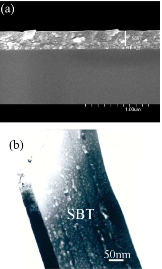
Fig. 1. (a) SEM and (b) TEM cross-section micrographs of SBT thin film pyrolyzed at 450◦C for 30 min.
SBT films were annealed at 450◦C by rapid thermal an-nealing furnace (RTA) in oxygen atmosphere for 5, 30, and 60 min, which has a very high heating and cooling rate of 100◦C/s. The surface microstructure of the SBT films was observed using atomic force microscopy (AFM, Digital Instrument Nano-Scope III). The thickness of SBT films is about 250 nm, as shown inFig. 1, which was examined by scanning electron microscopy (SEM, HITACHI-S4700) and transmission electron microscopy (TEM). The crystalline structure of SBT films was characterized by X-ray diffrac-tion (XRD). On the basis of XRD data, the average grain size can be determined by Scherrer’s formula. In order to measure the electrical properties of SBT thin films, 50 nm thick Pt top electrode with a diameter of 250m was sputter deposited using a shadow mask. The capacitance–voltage (C–V) characteristics of the MIM structure were measured
using the HP4284A LCR meter at 100 kHz as a function of a swept positive–negative voltage bias. The dielectric constant of the films was calculated from the capacitance measured at 100 kHz without bias voltage. The current density–electric field (J–E) measurements were performed by measuring the current through the sample using HP4156 with a delay time of 1 s. The P–E hysteresis loop of the films was traced using RT66A ferroelectric tester from Radiant Technologies.
3. Results and discussion
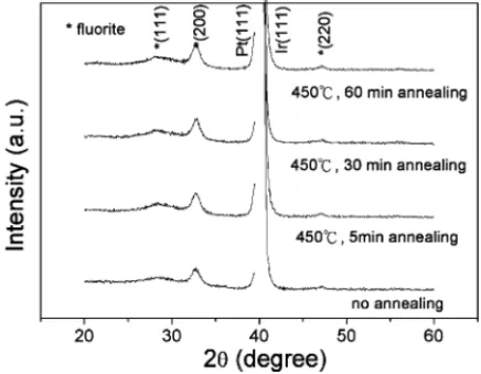
The XRD patterns of SBT-based MIM samples annealed at 450◦C for various times 0, 5, 30, and 60 min are shown inFig. 2. Clearly, the peaks are indicative of fluorite SBT phase, with (1 1 1), (2 0 0), and (2 2 0) orientations [9–11], and peaks corresponding to Ir(1 1 1, 2θ = 40.695) and Pt (1 1 1, 2θ = 39.798) phases [12]have also been observed. The effect of annealing time on the crystallinity improve-ment of the SBT films is minor. The intensity of preferred (2 0 0) peak of SBT films increases slightly with the nealing duration. The average grain size for SBT films an-nealed at 450◦C for 0, 5, 30, and 60 min are 4.6, 5.4, 5.7, and 6.0 nm, respectively. The SBT films annealed for longer annealing time have larger grain size compared with non-annealed or short time-annealed SBT.
Fig. 3 displays the AFM images of the SBT films py-rolyzed at 450◦C with and without annealing at 450◦C for 60 min. The surface roughnesses for SBT films with-out and with annealing at 450◦C for 60 min are 9.181 and 10.902 nm, respectively. Therefore, the surface rough-ness increases slightly with increasing annealing time. The surface of SBT film without annealing is smooth fluorite grains, but the surface of 60 min annealed SBT film reveals a few granular protrusions from the fluorite grain matrix. Such protrusive grains could be bismuth layered structure phase (i.e., Aurivillius grains), which were transferred from non-ferroelectric fluorite phase [13]. The larger surface
Fig. 2. XRD patterns of MIM structures based on fluorite-like SBT films.
Fig. 3. The AFM images of the MOD-derived SBT films pyrolyzed at 450◦C (a) without and (b) with annealing at 450◦C for 60 min.
roughness in the annealed SBT films is ascribed to the crystallization of Aurivillius phase and larger fluorite grain size.
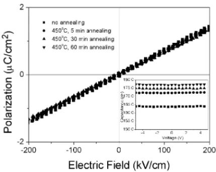
Fig. 4 illustrates the P–E curves recorded under a bias voltage of 5 V. It is indicated that the SBT films of cu-bic fluorite phase have linear dielectric property and does not have any ferroelectric characteristics, even for the sam-ples annealed for the longest duration of 60 min. As de-posited SBT films have a defective fluorite structure (Fig. 2), which have eight-fold coordination of the Ta ions, with eight nearest-neighbor oxygen ions. The actual structure has oc-tahedral six-fold coordination with two of these eight oxy-gen ions missing. Such fluorite structure possesses a center of inversion symmetry and is optically isotropic and conse-quently cannot possess polar properties or spontaneous po-larization [14]. The linear polarization of SBT films with
Fig. 4. Plots of polarization vs. electric field (P–E) of SBT films. The inset indicates capacitance–voltage (C–V) relations for SBT films annealed at various conditions.
cubic fluorite phase would be due to ionic polarizability and this polarization effects arises from the induced dipoles on both anions and cations, such as O−2, Sr+2, Bi+3, and Ta+5
[15]. The C–V plot in the inset ofFig. 4indicates that the annealing time affects the dielectric properties of the SBT films as samples annealed for longer durations exhibited bet-ter values of dielectric constant. The capacitance is inde-pendent of applied electric field as shown in inset ofFig. 4
by horizontal lines because no ferroelectric polarization and minor electrode barrier effect[16–18]. The higher dielectric constants (ε = 99, 100, and 101) of SBT films annealed for longer durations are attributed to better crystallization and larger grain size when compared with non-annealed SBT film (ε = 94).
The difference in the leakage current characteristics of the SBT films with various annealing conditions is shown in
Fig. 5. All the annealed SBT films possess current densities of 4× 10⁻⁸A/cm2 except for the non-annealed SBT film, which has a current density of 8×10⁻⁸A cm2at 200 kV cm. It is specified that the leakage current densities of annealed
Fig. 5. Leakage current density vs. electric field relations of the SBT films with various annealing conditions.
SBT films at 200 kV/cm are about double the magnitude lower than that of non-annealed SBT film. The lower leak-age current of SBT films annealed at 450◦C when compared to non-annealed SBT film may be attributed to reduction of defects of oxygen vacancies and hydrocarbon impurities of SBT films after annealing. Furthermore, the leakage current densities of SBT films annealed at 450◦C for various anneal-ing times maintain similar with increasanneal-ing annealanneal-ing time, because of the comparable values of the dielectric constant and grain size.
Fig. 6(a)shows a probability plot of approximately 20 test capacitors from four different samples to interpret the de-pendence of cumulative failure on dielectric breakdown field for 250 nm thick films annealed for various durations. This reliability test indicates that the longer the annealing time, the higher the breakdown fields in the fluorite-like SBT films possibly owing to the lower leakage current density and better crystallinity with larger dielectric constant. Lifetime extrapolation using constant voltage–stress time-dependent dielectric breakdown (TDDB) studies (Fig. 6(b)) indicates that the films with no annealing treatment have a life-time of over 10 years of operation at an electric field of 0.8 MV/cm.
Fig. 6. (a) Cumulative failure vs. breakdown field plots for non-annealed and annealed SBT film capacitors. (b) Time-dependent dielectric break-down for non-annealed SBT film.
4. Conclusions
The 450◦C low-temperature deposited non-ferroelectric fluorite-like SBT films fabricated by the MOD method in the present study have a suitable linear dielectric constant (ε ∼ 100), and very-low leakage current density of 4 × 10⁻⁸A/cm2 at 200 kV/cm. The linear polarization of SBT films would be due to ionic polarization effects arising from the induced dipoles on both anions and cations. For the fluorite-like SBT films, thermal annealing for different du-rations improves dielectric and electrical properties, but the crystallinity has minor dependence on annealing time, which have been demonstrated with the aid of property measure-ments (C–V, J–E, P–E) and XRD analysis, respectively. The dielectric constant increases from 94 to 101 and leakage cur-rent density decreases from 8× 10⁻⁸to 4× 10⁻⁸A/cm2at 200 kV/cm following the 450◦C annealing. In the reliability investigations of the cumulative failure of SBT breakdown filed and TDDB, we recognize that the SBT films possess breakdown field of 1.3 ∼ 2.1 MV/cm and lifetime of 10 years of operation at 0.8 MV/cm electric field.
Acknowledgements
The authors acknowledge the financial support from the National Science Council of the Republic of China under Project no. NSC 90-2215-E009-100.
References
[1] R.H. Dennard, Field effect transistor memory, US Patent 3,387,286 (4 June 1968).
[2] S. Ezhilvalavan, T.Y. Tseng, Appl. Phys. Lett. 74 (1999) 2477. [3] M.S. Tsai, S.C. Sun, T.Y. Tseng, J. Appl. Phys. 82 (1997) 3482. [4] Y.K. Wang, T.Y. Tseng, P. Lin, Appl. Phys. Lett. 80 (2002) 3790. [5] C.H. Huang, T.Y. Tseng, C.H. Chien, M.J. Yang, C.C. Leu, T.C.
Chang, P.T. Liu, T.Y. Huang, Thin Solid Films 420–421 (2002) 377. [6] T.Y. Tseng, S.Y. Lee, Appl. Phys. Lett. 83 (2003) 981.
[7] H.Y. Chou, T.M. Chen, T.Y. Tseng, Mater. Chem. Phys. 82 (2003) 826.
[8] H.Y. Chou, T.M. Chen, T.Y. Tseng, Key Eng. Mater. 247 (2003) 381. [9] K. Saito, M. Mitsuya, N. Nukaga, I. Yamaji, T. Akai, H. Funakubo,
Jpn. J. Appl. Phys. Part 1 (39) (2000) 5489.
[10] C.C. Leu, H.T. Lin, C.T. Hu, C.H. Chien, M.J. Yang, M.C. Yang, T.Y. Huang, J. Appl. Phys. 92 (2002) 1511.
[11] S.T. Tay, C.H.A. Huan, A.T.S. Wee, R. Liu, W.C. Goh, C.K. Ong, G.S. Cen, J. Vac. Sci. Technol. 20 (1) (2002) 125.
[12] PDF #461044(Ir) and #040802(Pt) Release 1998, JCPDS-ICDD, 1998.
[13] M. Moert, T. Mikolajick, G. Schindler, N. Nagel, W. Hartner, C. Dehm, Appl. Phys. Lett. 81 (2002) 4410.
[14] S.J. Hyun, B.H. Park, S.D. Bu, J.H. Jung, T.W. Noh, Appl. Phys. Lett. 73 (1998) 2518.
[15] M.J. Castiglione, M. Wilson, P. A Madden, J. Phys: Condens. Matter 11 (1990) 9009.
[16] S. Bhasker, S.B. Majumder, P.S. Dobal, S.B. Krupanidhi, R.S. Katiyar, Thin Solid Films 406 (2002) 30.
[17] S.M. Sze, Physics of Semiconductor Devices, second ed., Taipei, 1981, p. 555.
[18] K. Sreenivas, A. Mansingh, M. Sayer, J. Appl. Phys. 52 (11) (1987) 4475.