High quality Ge thin film grown by ultrahigh vacuum chemical vapor deposition on
GaAs substrate
Shih-Hsuan Tang, Edward Yi Chang, Mantu Hudait, Jer-Shen Maa, Chee-Wee Liu, Guang-Li Luo, Hai-Dang Trinh, and Yung-Hsuan Su
Citation: Applied Physics Letters 98, 161905 (2011); doi: 10.1063/1.3580605 View online: http://dx.doi.org/10.1063/1.3580605
View Table of Contents: http://scitation.aip.org/content/aip/journal/apl/98/16?ver=pdfcov Published by the AIP Publishing
Articles you may be interested in
Heteroepitaxy of GaAs on (001) 6° Ge substrates at high growth rates by hydride vapor phase epitaxy J. Appl. Phys. 113, 174903 (2013); 10.1063/1.4803037
Ge epitaxial films on GaAs (100), (110), and (111) substrates for applications of CMOS heterostructural integrations
J. Vac. Sci. Technol. B 31, 021203 (2013); 10.1116/1.4789427
Ultrathin low temperature SiGe buffer for the growth of high quality Ge epilayer on Si(100) by ultrahigh vacuum chemical vapor deposition
Appl. Phys. Lett. 90, 092108 (2007); 10.1063/1.2709993
Kinetics of Ge growth at low temperature on Si(001) by ultrahigh vacuum chemical vapor deposition J. Appl. Phys. 97, 064907 (2005); 10.1063/1.1854723
Growth and characterization of ultrahigh vacuum/chemical vapor deposition SiGe epitaxial layers on bulk single-crystal SiGe and Si substrates
J. Vac. Sci. Technol. A 20, 1120 (2002); 10.1116/1.1464840
This article is copyrighted as indicated in the article. Reuse of AIP content is subject to the terms at: http://scitation.aip.org/termsconditions. Downloaded to IP: 140.113.38.11 On: Wed, 30 Apr 2014 09:11:01
High quality Ge thin film grown by ultrahigh vacuum chemical vapor
deposition on GaAs substrate
Shih-Hsuan Tang,1Edward Yi Chang,1,2,a兲Mantu Hudait,3Jer-Shen Maa,1Chee-Wee Liu,4 Guang-Li Luo,5Hai-Dang Trinh,1and Yung-Hsuan Su1
1
Department of Materials Science and Engineering, National Chiao Tung University, 1001 Ta-Hsueh Rd., Hsin-chu 300, Taiwan
2
Department of Electronics Engineering, National Chiao Tung University, 1001 Ta-Hsueh Rd., Hsin-chu 300, Taiwan
3
Department of Electrical and Computer Engineering, Virginia Tech, Blacksburg, Virginia 24061, USA 4
Department of Electrical Engineering, National Taiwan University, Taipei 106, Taiwan 5
National Nano Device Laboratories, Hsin-chu 300, Taiwan
共Received 10 January 2011; accepted 28 March 2011; published online 19 April 2011兲
High-quality epitaxial Ge films were grown on GaAs substrates by ultrahigh vacuum chemical vapor deposition. High crystallinity and smooth surface were observed for these films by x-ray diffraction, transmission electron microscopy, and atomic force microscopy. Direct band gap emission共1550 nm兲 from this structure was detected by photoluminescence. Valence band offset of 0.16 eV at the Ge/GaAs interface was measured by x-ray photoelectron spectroscopy. N-type arsenic self-doping of 1018/cm−3in the grown Ge layers was determined using electrochemical capacitance voltage measurement. This structure can be used to fabricate p-channel metal-oxide-semiconductor field-effect transistor for the integration of Ge p-channel device with GaAs n-channel electronic device. © 2011 American Institute of Physics.关doi:10.1063/1.3580605兴
In the past several decades, there has been a steady step-up of device performance along with the continued re-duction in device feature sizes for silicon devices. Further-more, for small feature size silicon devices, additional gain-ing in carrier mobility can be achieved by applygain-ing a strain to the channel material.1In contrast to these Si devices, high-speed devices made from III–V materials are characterized with a high electron mobility but still suffer from low hole mobility. Therefore, it is still a challenge to find a p-channel material with high hole mobility.
The epitaxial Ge layer on GaAs substrate as the p-channel material for complementary III–V CMOS logic is studied in this letter. In the past few years, devices with Ge channel material on Si substrate have been fabricated, and a higher p-channel hole mobility has been reported.2 The in-creasing interest to pursue this Ge/GaAs approach is due to the following reasons: 共1兲 Ge has a much higher bulk hole mobility 共h= 1900 cm2/V s兲 as compared to GaAs 共h
= 400 cm2/V s兲, 共2兲 the Ge/GaAs interface has a very small
lattice mismatch 共⬃0.08%兲, therefore thicker Ge films can be grown on GaAs substrates with very low threading dislo-cation density, and 共3兲 the narrower band gap of Ge 共Eg
= 0.66 eV兲 lies within a wider band gap of GaAs 共1.42 eV兲, resulting in a good confinement of carriers in the Ge layer.3 In this work, high-quality epitaxial Ge films were depos-ited on GaAs by ultrahigh vacuum chemical vapor deposi-tion 共UHVCVD兲. In-depth characterizations of film struc-ture, optical and electrical properties, and doping conditions were carried out using methods of x-ray diffraction共XRD兲, cross-sectional transmission electron microscopy 共TEM兲, atomic force microscopy 共AFM兲, photoluminescence 共PL兲, x-ray photoelectron spectroscopy 共XPS兲, and
electrochemi-cal capacitance voltage共ECV兲 profiling. The purpose of this study is to evaluate Ge film on GaAs for potential Ge/GaAs p-channel electronic devices with high hole mobility for fu-ture integration with Si technology.
Epiready GaAs共100兲 wafers were used as substrates for Ge deposition. Ge deposition was carried out in an UH-VCVD system using GeH4as Ge source. Before deposition,
the as-received GaAs wafer was loaded into the load-lock chamber without any precleaning step. After the pressure of load-lock reached 2⫻10−6 Torr, the wafer was then trans-ferred into the deposition chamber. The wafer then went through a prebake step and the native oxide 共As2O3 and
Ga2O3兲 on the surface were removed in this step. Due to the sensitive nature of GaAs substrate surface, the prebake time without arsenic overpressure was controlled carefully to pre-vent the decomposition of GaAs. The GaAs substrate was annealed at 600 ° C for 2 min prior to GeH4flow. The GeH4 flow was fixed at 10 SCCM共SCCM denotes cubic centime-ter per minute at STP兲, the pressure was controlled at 20 mTorr, and deposition time was varied to deposit undoped Ge films to the thicknesses of 200 nm, 450 nm, and 2.75 m.
The structural and crystalline qualities of the films were analyzed by high-resolution XRD 共HRXRD兲 and cross-sectional TEM. The surface roughness was determined by AFM. PL measurement was used to determine the emission and the band gap of the material, the ECV profiler was used to determine the doping type and background concentration. XPS was used to determine the valence band offset 共⌬Ev兲
between the Ge film and the GaAs substrate.
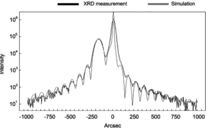
The 200 nm thick Ge film deposited at 600 ° C on GaAs substrate was used for the HRXRD measurement using a Bede D1 XRD system. The scanned result is shown in Fig.1, in which the HRXRD result is in black line and the simulated curve is in gray line, with the GaAs substrate peak at zero. The angle between the peaks of the Ge film and the GaAs
a兲Author to whom correspondence should be addressed. Electronic mail:
APPLIED PHYSICS LETTERS 98, 161905共2011兲
0003-6951/2011/98共16兲/161905/3/$30.00 98, 161905-1 © 2011 American Institute of Physics
This article is copyrighted as indicated in the article. Reuse of AIP content is subject to the terms at: http://scitation.aip.org/termsconditions. Downloaded to IP: 140.113.38.11 On: Wed, 30 Apr 2014 09:11:01
substrate is less than 200 arc sec. The HRXRD result and the simulated curve match closely with each other. The appear-ance of fringes on both sides of Ge and GaAs peaks implies a parallel and very sharp interface existed in this heterojunc-tion structure.2 AFM measurement of the same structure shows that the root mean square roughness 共rms兲 was only 0.132 nm and the mean surface roughness 共Ra兲 was about 0.104 nm. All these indicate that the Ge film grown on GaAs substrate was very uniform and can be used for the fabrica-tion of metal-oxide-semiconductor field-effect transistor 共MOSFET兲 or p-channel quantum well devices.
The crystalline quality of thicker Ge film was further characterized by cross-sectional TEM. Figure 2 is a cross-sectional TEM micrograph of 2.75 m thick Ge film depos-ited on GaAs substrate grown at 600 ° C. A few misfit dislo-cations are detected at the interface, but there is no appearance of any threading dislocation, which is expected. The lattice mismatch between these two materials is ex-tremely small, which is 0.08% at room temperature and about 0.1% at growth temperature. The distance between two misfit dislocations is about 400 nm. Since the lattice con-stants of Ge and GaAs are 5.64 613 Å and 5.65 33 Å, respec-tively, therefore at the interface there are 708 lattices of Ge to match 707 lattices of GaAs at the interface. This means that for every 400 nm, an atom from the GaAs lattice is missing
to form the string of one misfit dislocation. The high reso-lution TEM graph 共the inset of Fig. 2兲 shows very good interface quality between Ge and GaAs.
Recently, a direct band gap emission has been observed with the structure of Ge on Si.4–6To obtain this emission, it requires the application of a tensile strain of under 2% to the Ge film,7,8 a high pumping level, high temperature, and a n-type doping of Ge to compensate the 0.136 eV difference in energy between⌫ and L valleys.9In one report, in order to increase the electron fraction of ⌫ valley and to move the Fermi level upwards,6 the pump power was raised to 360 mW at room temperature. The direct radiative transition rate is about 1600 times that of the indirect transition at high power excitation.10 The PL spectrum of Ge on GaAs is shown in Fig. 3. This is a room temperature PL infrared emission with 671 nm incident. The PL peak at 1550 nm, corresponding to an energy of 0.8 eV, reveals that the elec-trons in L valley recombine with holes in the valence band, the direct band gap emission occurs in the 200 nm Ge film on GaAs substrate.
In order to understand the mechanism of PL emission from the Ge sample, a Ge film with 450 nm in thickness was prepared for accurate ECV measurement to determine the type of Ge film. The result is shown in the inset of Fig. 3. The Ge film is n-type with a donor concentration of 2.49 ⫻1018/cm3.
The reason that the direct band emission of Ge on GaAs substrate can be detected is probably related to the high qual-ity of epitaxial Ge film on GaAs and the unexpected n-type doping. By filling 2.49⫻1018/cm3 electrons into L valley,
the energy difference between ⌫ valley and L valley can be compensated mostly. The band gap of L valley and the band gap of ⌫ valley becomes almost the same because the elec-trons filled the ⌫ valley, and some electrons injected and existed in the⌫ valley. The electrons in the ⌫ valley recom-bine with holes, emitting light of direct transition at 1550 nm. The theory mentioned above is discussed in pervious study.9 The arsenic donor was from the memory doping in the chamber which was caused by the decomposition of GaAs. The memory doping was confirmed by the horizontal profile of the donor concentration in ECV curve. This n-type Ge film can be used for the fabrication of the p-channel MOSFET, the advantage is that a Ge p-channel device can be processed adjacent to a GaAs n-channel device in a simple integration process.
FIG. 1. XRD measurement of 200 nm Ge film on GaAs substrate. The fringes on both sides imply a sharp Ge/GaAs interface.
FIG. 2. 共Color online兲 Cross-sectional TEM image of Ge on GaAs. A few misfit dislocations are seen at the interface but no threading dislocation is detected. The inset is the high resolution TEM.
FIG. 3. 共Color online兲 Room temperature PL infrared emission from the structure of 200 nm Ge film on GaAs substrate. The direct band gap emis-sion occurs at 1550 nm with energy of 0.8 eV. The ECV data shows that the Ge film is n-type, and the donor concentration is about 2.49⫻1018/cm3.
161905-2 Tang et al. Appl. Phys. Lett. 98, 161905共2011兲
This article is copyrighted as indicated in the article. Reuse of AIP content is subject to the terms at: http://scitation.aip.org/termsconditions. Downloaded to IP: 140.113.38.11 On: Wed, 30 Apr 2014 09:11:01
The valence band offset共⌬Ev兲 at the Ge/GaAs interface was determined from XPS measurements of the binding en-ergy of core level and valence band maximum 共VBM兲. The valence band offset value can be determined with the equa-tion by Kraut et al.,11
⌬EV=共EAs 3d− EVBM兲 − 共EGe 2d− EVBM兲
+共EGe 2d− EAs 3d兲.
⌬EVis determined from the difference between As 3d
core level 共EAs 3d兲 and VBM 共EVBM兲 of GaAs film, As 3d
core level 共EAs 3d兲 and Ge 2d core level 共EGe 2d兲 at Ge/ GaAs interface, Ge 2d core level共EGe 2d兲 and VBM 共EVBM兲
of Ge film. In order to measure the binding energy and VBM, XPS measurements were carried out on two Ge films with thicknesses of 10 nm and 100 nm, respectively, grown on GaAs substrates together with one piece of pure GaAs wafer. Figure4shows the XPS spectra of As 3d core level共EAs 3d兲 and VBM 共EVBM兲 of GaAs film, As 3d core level 共EAs 3d兲
and Ge 2d core level共EGe 2d兲 at Ge/GaAs interface, Ge 2d
core level 共EGe 2d兲 and VBM 共EVBM兲 of Ge film. The values of EAs 3d− EVBM, EGe 2d− EVBM, and EGe 2d− EAs 3dare 41.25
eV, 29.81 eV, and ⫺11.6 eV, respectively. The value of va-lence band offset共⌬Ev兲 at the Ge/GaAs interface is 0.16 eV which is consistent with the theoretical value proposed by Kraut et al.11From these measurements, it is further proved that the Ge/GaAs structure can be used for heterojunction devices such as p-channel quantum well devices.
High quality Ge films were grown on GaAs substrate by UHVCVD, as confirmed by XRD and TEM. The film thick-ness was uniform with smooth interface, as indicated by AFM and HRXRD. A direct band gap emission共1550 nm兲 of Ge epitaxial layer/GaAs substrate was detected by PL and ECV measurement showed the grown Ge layers were n-type doped with arsenic self-doping concentration of 1018/cm−3. The valence band offset 共⌬Ev兲 at the Ge/GaAs interface is 0.16 eV which is consistent with the theoretical value. This structure studied is useful for the future integration of Ge p-channel and GaAs n-channel electronic devices on Si tem-plate.
1S. E. Thompson, M. Armstrong, C. Auth, S. Cea, R. Chau, G. Glass, T.
Hoffman, J. Klaus, M. Zhiyong, B. Mcintyre, A. Murthy, B. Obradovic, L. Shifren, S. Sivakumar, S. Tyagi, T. Ghani, K. Mistry, M. Bohr, and Y. El-Mansy,IEEE Electron Device Lett. 25, 191共2004兲.
2M. Zhu, H. C. Chin, G. S. Samudra, and Y. C. Yeo,J. Electrochem. Soc. 155, H76共2008兲.
3R. Haight and J. A. Silberman,Appl. Phys. Lett. 57, 1548共1990兲. 4M. El Kurdi, T. Kociniewski, T. P. Ngo, J. Boulmer, D. Débarre, P.
Bou-caud, J. F. Damlencourt, O. Kermarrec, and D. Bensahel,Appl. Phys. Lett. 94, 191107共2009兲.
5W. Klingenstein and H. Schweizer,Solid-State Electron. 21, 1371共1978兲. 6X. Sun, J. Liu, L. C. Kimerling, and J. Michel, Appl. Phys. Lett. 95,
011911共2009兲.
7R. Soref, J. Kouvetakis, and J. Menendez, Advances in SiGeSn/Ge Tech-nology, MRS Symposia Proceedings No. 958共Materials Research Society,
Pittsburgh, 2007兲, p. 13.
8J. Menéndez and J. Kouvetakis,Appl. Phys. Lett. 85, 1175共2004兲. 9J. Liu, X. Sun, P. Becla, L. C. Kimerling, and J. Michel, Fifth IEEE
International Conference on Group IV Photonics共IEEE, New York, 2008兲,
pp. 16–18.
10T. H. Cheng, C. Y. Ko, C. Y. Chen, K. L. Peng, G. L. Luo, C. W. Liu, and
H. H. Tseng,Appl. Phys. Lett. 96, 091105共2010兲.
11E. A. Kraut, R. W. Grant, J. R. Waldrop, and S. P. Kowalczyk,Appl. Phys. Lett. 44, 1620共1980兲.
FIG. 4. 共Color online兲 XPS spectra of 共1兲 As 3d core level 共EAs 3d兲 and
VBM共EVBM兲 of GaAs film, 共2兲 As 3d core level 共EAs 3d兲 and Ge 2d core
level共EGe 2d兲 at Ge/GaAs interface, and 共3兲 Ge 2d core level 共EGe 2d兲 and VBM共EVBM兲 of Ge film.
161905-3 Tang et al. Appl. Phys. Lett. 98, 161905共2011兲
This article is copyrighted as indicated in the article. Reuse of AIP content is subject to the terms at: http://scitation.aip.org/termsconditions. Downloaded to IP: 140.113.38.11 On: Wed, 30 Apr 2014 09:11:01