國
立
交
通
大
學
資訊科學與工程研究所
碩
士
論
文
資料位址預測以用來對第一階快取記憶體做電源
管理
Data Address Prediction for L1 Data Cache Power Mode
Management
研 究 生:莊富元
指導教授:單智君 教授
資 料 位 址 預 測 以 用 來 對 第 一 階 快 取 記 憶 體 做 電
源 管 理
Data Address Prediction for L1 Data Cache Power Mode Management
研 究 生:莊富元 Student:Fu-Yuan Chuang
指導教授:單智君 Advisor:Jean Jyh-Jiun Shann
國 立 交 通 大 學
資 訊 科 學 與 工 程 研 究 所
碩 士 論 文
A Thesis
Submitted to Institute of Computer Science and Engineering College of Computer Science
National Chiao Tung University in partial Fulfillment of the Requirements
for the Degree of Master
in
Computer Science
Sept. 2006
Hsinchu, Taiwan, Republic of China 中華民國九十五年九月
資 料 位 址 預 測 以 用 來 對 第 一 階 快 取 記 憶 體 做 電 源 管 理
學生:
莊富元指導教授
:單智君 博士國立交通大學資訊科學與工程學系﹙研究所﹚碩士班
摘 要處理器內部的快取記憶體的耗電在整顆處理器的耗電上佔了相當大
的比例。隨著製程的進步,靜態耗電的比例會逐漸上升。目前有一個
稱之為 drowsy cache 的技術(每個快取記憶體區塊都有兩種不同的電
壓可供選擇)可以有效降低在快取記憶體中的靜態耗電。然而,要喚醒
一個處於 drowsy 狀態的快取記憶體區塊需要消耗額外的時間及能量。
而且這個額外的時間會導致整個系統的靜態耗電跟著消耗。本篇論文
提出一套預測資料位址的策略,利用該策略來預先打開即將要被存取
到的資料快取記憶體。實驗結果顯示,利用我們所提出的這個策略,
並與前人的研究做相比,可更進一步地節省資料快取記憶體 3%左右的
靜態耗電。
Data Address Prediction for L1 Data Cache Power Mode Management
student:
Fu-Yuan ChuangAdvisors:Dr.
Jean Jyh-Jiun ShannDepartment﹙Institute﹚of
Computer Science and EngineeringNational Chiao Tung University
ABSTRACT
On-chip cache is a major chip power consumer. Due to nanoscale
technology, the dominant of this power loss will be leakage. The drowsy
cache scheme, where one can choose between two different supply
voltages in each cache line, is a technique that reduces the leakage energy
for cache. Yet, waking up a drowsy line needs extra time and energy, and
this extra time would result in total static power consumption. This paper
proposes one data address prediction and exploits it to preactivate
oncoming cache lines before access requests. Our experimental results
indicate that the proposed preactivation policy reduces the power
consumption by about 3% (assuming 70nm technology) with respect to
previously proposed drowsy cache policies.
誌謝
首先我要感謝我的指導老師 單智君老師,在這兩年的時間內,老
師給了我許多寶貴的建議及嚴謹的指導,讓我得以順利的完成這篇論
文。除了學業上的指導,也從老師身上學習了許多一生中受用的道理。
另外,我想感謝本實驗室另一位老師 鍾崇斌老師。鍾老師除了擔任我
的口試委員外,在我兩年碩士生活中,也給了我許多寶貴的指導。還
有另一位口試委員 謝萬雲老師,在口試時給了許多明確的指點,讓我
的碩士論文更佳的完整。
還要謝謝實驗室的學長及同學們,花了許多時間細心地和我討論,並
給了許多建議。實驗室所有成員與我一起渡過的時光以及一起討論課
業的情景,我永遠不會忘記。
最後我要感謝我的家人,長久以來毫無保留的給予我支持與鼓勵,讓
我能在你們的關心之中順利的完成學業。
謝謝你們!
莊富元
2006 年九月
Table of contents
CHAPTER 1 INTRODUCTION 1
1.1 IMPORTANCE OF LOW POWER DESIGN... 1
1.1.1 Importance of low power design ... 1
1.1.2 Main power components of CMOS circuits:... 2
1.2 IMPORTANCE OF LOW POWER DESIGN FOR DATA CACHE... 3
1.3 LEAKAGE ENERGY REDUCTION OF CACHE... 4
1.4 DATA ADDRESS PREDICTION... 6
1.5 MOTIVATION &OBJECTIVE... 6
CHAPTER 2 BACKGROUND AND RELATED WORK 8 2.1 BACKGROUND... 8
2.1.1. Researches on static power reduction ... 8
2.1.2. An effective data address predictor ... 10
2.2 RELATED WORK... 11
2.2.1. Drowsy cache ... 12
2.2.2. Compiler approach ... 14
2.2.3. A Preactivating Mechanism for a VT-CMOS Cache ... 20
2.2.4. Summary and Observation... 24
CHAPTER 3 PROPOSED DESIGN 26 3.1. DATA ADDRESS PREDICTION... 26
3.1.1. Basic Idea of data address prediction ... 26
3.1.2. Design issue ... 27
3.1.3. Block Diagram of Data Address Prediction Hardware ... 28
3.1.4. Prediction mechanism ... 29
3.1.5. The flow chart and implementation for our data address prediction... 35
3.2. PRE-ACTIVATION POLICY... 37 3.3. DE-ACTIVATION POLICY... 39 CHAPTER 4 EVALUATION 40 4.1 EXPERIMENT METHODOLOGY... 40 4.2 EVALUATION METRICS... 41 4.3 EXPERIMENT RESULTS... 43 4.3.1 Prediction result... 43
4.3.2 Leakage energy result... 49
CHAPTER 5 CONCLUSION 54 CHAPTER 6 REFERENCE 55
List of Figures
1-1 Trends in Power across Process Technologies ………...3
2-1 Block Diagram and State Transition Diagram for a Simple Stride-based Value Predictor ………...11
2-2 Implementation of the Drowsy Cache Line ………...13
2-3 Relevant Cache Lines (RCLs) for an Object in a Direct-mapped Data ………...16
2-4 An Example Code Fragment (a), and its Transformed Versions (b) and (c) ……19
2-5 Circuit of a Line in the Original DLC ………...21
2-6 Processor Organization with a Preactivating DLC Cache ………...22
2-7 Circuit of a Line in The Preactivating DLC Cache ………..22
2-8 Accesses Time of DLC and Non-DLC Caches ………24
3-1 Block Diagram of Data Address Prediction ………...29
3-2 DAST Mode Transition Diagram ……….30
3-3 Predict the Next Used Data Address When DAST Is in Match Mode …………30
3-4 Predict the Next Used Data Address When DAST Is in Verify mode ………….31
3-5 Predict the Next Used Data Address When DAST Is in Verify mode ………….32
3-6 Overview of Smart Table ………...34
3-7 Instruction Execution Path ………...35
3-8 Flow Chart of Our PreactivationPolicy ………...36
3-9 Implementation of Data Address Prediction Hardware ………...37
3-10 Implementation of Preactivation Policy ………...38
4-1 Define Ideal Case ……….42
4-2 Offset Values Percentage for Auto-Indexed Load/Store Instructions ………...43
4-3 Stride Values Percentage for Non Auto-Indexed Load/Store Instructions …...44
4-4 Instruction Percentage and Its Data Address Behavior ………45
4-5 Prediction Accuracy of Top Hit and Bottom Hit ……….46
4-6 Prediction Coverage, Accuracy, and Multiple hit for top hit ………...47
4-7 Prediction Coverage, Accuracy for DAST and VHT ………...48
4-8 Leakage Energy for Simple Policy and Noaccess Policy ………49
4-10 Normalized Leakage Energy for Each Policy ………...52 4-11 Performance Loss for Each Policy ………53
List of Tables
1-1 Circuit Techniques of Controlling Cache Leakage ………5 2-1 Impact of Activate/Deactivate Instructions on Different Cache
Line States ………....17 2-2 Summary of Related Works ……….… 25 4-1 Base Configuration Parameters and Their Values in Our Base ………...41
Chapter 1 Introduction
Reducing power consumption is important for both battery-operated
embedded/mobile devices and high-end machines. Generally, the power components of CMOS circuits can be classified into two parts: dynamic and static. The latter will exceed the former to be a major consumer as technology drops below the 65-nm feature size. Since the caches constitute a significant portion of the transistor budget of current microprocessors, static power reduction of cache is especially important. Besides, because data address has locality property, we could use this property to do data address prediction.
1.1 Importance of low power design
In this section, we will discuss the importance of low power design and review the power components of CMOS circuits.
1.1.1 Importance of low power design
Power dissipation has become a significant constraint in modern microprocessor design. In battery-operated embedded/mobile devices and high-end machines, power is already the leading design constraint. It has become one of the primary design
constraints along with performance, clock frequency, and die size. In battery-operated devices, high power consumption would mainly reduce the battery lifetime. In case of high-end machines, high power consumption would lead to thermal issues like device degradation, higher packaging cost, and reduced chip lifetime. Consequently, overall product quality is highly dependent on techniques for minimizing system power consumption. These techniques can be applied on various design abstraction levels,
from circuit level to system architecture. Circuit-level power minimization techniques have played the predominant role in designing energy efficient ICs. However,
architecture-level approaches are starting to attain popularity in recent years, thus resulting in even greater power optimizations.
1.1.2 Main power components of CMOS circuits:
Total power is growing exponentially with each process generation. Generally, the power components of CMOS circuits include both dynamic and static power. Dynamic, or active, power is consumed while the device is in operation. Static, or leakage, power is consumed by leakage current in non-ideal transistor operations, i.e., incomplete turning off. Dynamic power could be classified into two parts: switch power and short-circuit power. Switch power is the power dissipated by charging and discharging the load capacitances in circuits. Short-circuit power is the power dissipated by
momentary short circuit at a gate’s output whenever the gate switches, and this power is relatively small.
In the previous generation of CMOS technology, dynamic power had large impact on total chip power. However, with the increasing number of transistors employed in a chip and the continued reduction in threshold voltages of these transistors, leakage power has become a major concern. Figure 1-1 shows the trends in power across process technologies. We can see that static power will exceed dynamic power as technology drops below the 65-nm feature size.
1.2 Importance of low power design for data cache
The instruction/data cache subsystem is an important microarchitecture component serving to bridge the ever growing gap between memory access time and processor execution speed. Not only the increasing variance between processor speed and memory access time, but also application complexity constitute driving forces toward larger caches implemented on the same die as the microprocessor core. Both tag and data arrays are placed on the processor’s die and typically account for a significant part of the transistor budget and hence of the total power consumption. For example, the Intel Pentium Pro dissipates 33% [2] and the StrongARM-110 dissipates 42% [3] of its total power in on-chip caches. The instruction cache is under heavy utilization in every processor cycle; the data cache exhibits similar high utilization especially in the case of data intensive multimedia applications and very long instruction word processor
architectures, which exploit a high amount of instruction level parallelism.
Since the caches constitute a significant portion of the transistor budget of current microprocessors, leakage energy reduction for cache is especially important. For
instance, in the case of a 0.07μ process technology, it has been estimated that leakage m energy of cache accounts for 70% of total cache energy [4]. Since the size of data cache is about the half of total cache in many systems, reducing leakage energy of data cache is important.
1.3 Leakage energy reduction of cache
Cache access has locality property. In other words, the activity in a cache is only centered on a small subset of the lines during a fixed period time. If we can use some techniques (such as decreasing supply voltage or increasing threshold voltage) for those unused cache lines, we can reduce leakage energy of cache.
Two broad categories of circuit techniques aim to reduce leakage: state-destructive and state-preserving:
State-destructive techniques use ground gating, also called gated-Vdd. Ground
gating adds an NMOS (n-channel metal-oxide semiconductor) sleep transistor to connect the memory storage cell and the power supply’s ground [5][6][7]. Turing a cache line off saves maximum leakage power, but the loss of state exposes the system to incorrect turn-off decisions. Such decisions can in turn induce significant power and performance overhead by causing additional cache misses that off-chip memories must satisfy.
State-preserving techniques have two. One is drowsy cache [8], the other is DLC
(dynamic leakage cut-off) cache [9]. Drowsy caches multiplex supply voltages according to the state of each cache line or block. The caches use a low-retention voltage level for drowsy mode, retaining the data in a cache region and requiring a high voltage level to access it. Waking up the drowsy cache line is treated as a pseudo cache miss and incurs one additional cycle overhead. DLC cache saves leakage energy by
controlling transistors’ threshold voltage by the line on demand. In other words, the threshold voltages of transistors in a cache line are high to suppress leakage current. When one cache line needs to be activated, the threshold voltage of transistors in that line changes to a low voltage.
The above two techniques reduce leakage less than turning a cache line off completely, but accessing the low-leakage state incurs much less penalty. Moreover, while state-preserving techniques can only reduce leakage by about a factor 10,
compared to more than a factor a 1,000 for destructive techniques, the net difference in power consumed by the two is less than 10 percent. When the reduced wake-up time is factored into overall program runtime, state-preserving techniques usually perform better. They have the additional benefit of not requiring an L2 cache.
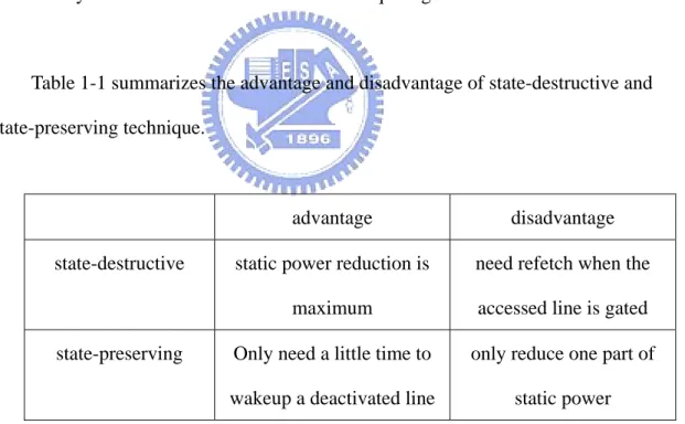
Table 1-1 summarizes the advantage and disadvantage of state-destructive and state-preserving technique.
advantage disadvantage
state-destructive static power reduction is maximum
need refetch when the accessed line is gated state-preserving Only need a little time to
wakeup a deactivated line
only reduce one part of static power
In this paper, we adopt one state-preserving circuit technique - drowsy cache (change supply voltage). The reason why we do not adopt DLC cache (change threshold voltage) is that the time of waking up a deactivated line is longer than drowsy cache.
1.4 Data address prediction
In this section, we briefly introduce the concept of how data address is predicted. In section 2.1.2, we will introduce an effective data address predictor.
Many load/store instructions are used to access array elements and scalar data, and this phenomenon is more obvious in embedded applications. That is, data address has locality property because of loop induction variables and programs stepping through arrays in a regular fashion. Data address locality is captured by monitoring the stride by which the data address of consecutive instances of an instruction change. If the data addresses vary by a constant stride, then it is easy to predict the results of future instances of that instruction.
The essence of data address prediction is to predict the effective address of load/store instructions based on their past behavior. Exploiting the above data address locality, we could easily predict the data address of next execution of one load/store instruction.
1.5 Motivation & Objective
Since waking up a drowsy data cache line needs extra time, propose a pre-activation mechanism for data cache to suppress this penalty. To propose a
pre-activation mechanism for data cache, data address prediction is essential. Since data address has locality property, that is, the data address difference between two
consecutive executions of one load/store instruction is often a constant value. Exploiting the data address locality, we could predict the data address of next execution of one load/store instruction. In addition, reserve predicted data address sequence, and when data address generated by one load/store instruction could be found in this sequence, we would pre-activate the next used cache line if it is a low-powered line.
So, our objective is to propose a pre-activation mechanism to co-work with drowsy data cache to decrease static power dissipation and performance loss.
Chapter 2 Background and Related Work
In section 2.1, we will review some backgrounds on how to reduce static power from the view of equation and an effective data address prediction. In section 2.2, we will introduce three researches on reducing data cache leakage energy.
2.1 Background
Now, we briefly introduce static power equation and researches on static power reduction. Besides, we also introduce an effective mechanism on data address prediction.
2.1.1. Researches on static power reduction
The following equation defines static power consumption. Static power loss is due to leakage current, Ileak.
s leak
P =VI (1) (Ps: static power; V: transistor’s supply voltage; Ileak: leakage current)
As noted, leakage current, the source of static power consumption, is a combination of subthreshold and gate-oxide leakage: Ileak =Isub+Iox.
Subthreshold power leakage
th
V / nV V / V
sub 1
I =K We− θ(1 e− − θ) (2)
1
the thermal voltage. At room temperature, Vθis about 25mV; it increases linearly as temperature increases. If Isubgrows enough to build up heat, Vθwill also start to rise, further increasing Isuband possibly causing thermal runaway.
Equation 2 suggests two ways to reduceIsub. First, we could turn off the supply voltage-that is, set V to zero so that the factor in parentheses also becomes zero. Second, we could increase the threshold voltage, which-because it appears as a negative exponent-can have a dramatic effect in even small increments.
Equation 3 shows the dependency of operating frequency on supply voltage and threshold voltage.
th
f ∞ (V−V ) / Vα (3)
We know from equation 3 that increasingV will reduce speed. The problem with th the first approach is loss of state; the problem with the second approach is the loss of performance.
Gate width W is the other contributor to subthreshold leakage in a particular
transistor. Designers often use the combined widths of all the processor’s transistors as a convenient measure of total subthreshold leakage.
Gate-oxide power leakage
ox T / V 2 ox 2 ox V I K W( ) e T −α = (4) 2
K andαare experimentally derived. The term of interest is oxide thickness, T . ox Clearly, increasingT will reduce gate leakage. Unfortunately, it also degrades the ox transistor’s effectiveness becauseT must decrease proportionally with process scaling ox
to avoid channel effects. Therefore, increasingT is not an option. The research ox community is instead pursuing the development of high-k dielectric gate insulators.
As with subthreshold leakage, a die’s combined gate width is a convenient measure of total oxide leakage.
2.1.2. An effective data address predictor
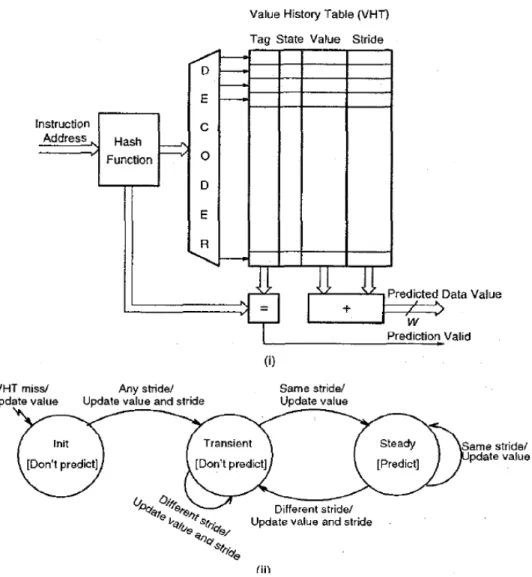
A stride-based predictor is proposed by K. Wang et al [10]. The essence of data address prediction is to predict the result of load/store instructions based on their past behavior; just like predicting the outcome of conditional branches. A good heuristic to use is to record the recent results produced by previous instances of an instruction, and predict the result of the instruction’s next instance based on past results.
Figure 2-1(i) gives a block diagram of a simple stride-based value predictor. Its VHT entry has 4 fields-Tag, State, Value, and Stride. The state can have one of 3 states-Init, Transient, and Steady. The state transition diagram is given in Figure 2-1(ii). The basic step in a stride-based predictor is the stride detection phase, which aims at detecting a stride sequence. The first time an instruction is encountered (as evident from a miss in the VHT), no prediction is made. When the instruction produces its result, an entry is allocated in the VHT, and the following actions take place: (i) the result is stored in the Value field of that entry, and (ii) the State of that entry is set to Init. While in the Init state, if another instance of the same instruction is encountered, no prediction is made. However, when that instance produces a result (D1), that is potentially the beginning of a stride sequence, and the following actions take place: (i) the stride is calculated as S1 = D1 – Value in VHT entry, (ii) D1 and S1 are entered in the Value and
Stride fields of the VHT entry, and (iii) the State is set to Transient. While in Transient state, if another instance of the same instruction is encountered, no prediction is made.
When that instance produces a result (D2), the following actions take place: (i) the stride is calculated as S2 = D2 – Value in VHT entry, (ii) D2 is entered in the Value field of the VHT entry, and (iii) if S2 is same as previous stride, the State is set to Steady, else S2 is entered in the Stride field. While in the Steady state, predictions are made by adding together the Value and Stride fields; if a different stride appears, then the State is set to Transient. This simple 3-state scheme can detect most strides.
2.2 Related work
Figure 2-1: Block Diagram and State Transition Diagram for a Simple Stride-based Value Predictor
of first paper could also be applied for instruction cache. The methodologies of the last two papers are dedicated for data cache. The second proposes a pre-activation
mechanism based on drowsy cache. The third proposes a pre-activation mechanism based on DLC cache.
2.2.1. Drowsy cache
K. Flautner [8] et al. propose a simple technique for reducing leakage power called drowsy cache, where one can choose between two different supply voltages in each cache line. Their idea is put those unused cache lines into low-power drowsy mode to reduce leakage energy of cache.
2.2.1.1. Power control scheme
Approaches for reducing static power consumption of caches by turning off cache lines using the gated-Vdd technique [5] has been described in [6]. These approaches
reduce leakage power by selectively turning off cache lines that contain data that is not likely to be reused. The drawback of this approach is that the state of the cache line is lost when it is turned off and reloading it from the level 2 cache has the potential to negate any energy savings and have a significant impact on performance. To avoid these pitfalls, it is necessary to use complex adaptive algorithms and be conservative about which lines are turned off.
Turning off cache lines is not the only way that leakage energy can be reduced. Significant leakage reduction can also be achieved by putting a cache line into a low-power drowsy mode. When in drowsy mode, the information in the cache line is preserved; however, the line must be reinstated to a high-power mode before its contents can be accessed. To be this purpose, propose a simpler and more effective
circuit technique for implementing drowsy caches, where one can choose between two different supply voltages in each cache line. That is, exploiting voltage scaling to reduce static power consumption. Due to short-channel effects in deep-submicron processes, leakage current reduces significantly with voltage scaling. The combined effect of reduced leakage current and voltage yields a dramatic reduction in leakage power. Moreover, the penalty for waking up a drowsy line is relatively small (it requires little energy and only 1 or 2 cycles, depending on circuit parameters).
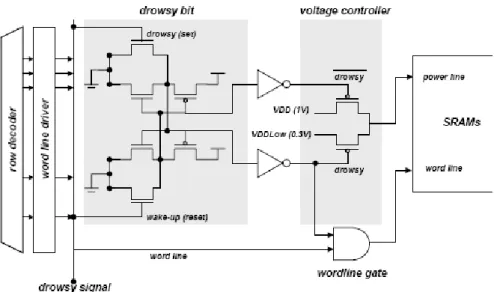
Figure 2-2 shows the changes necessary for implementing a cache line that
supports a drowsy mode. There are few additions required to a standard cache line. The main additions are a drowsy bit, a mechanism for controlling the voltage to the memory cells, and a word line gating circuit. In order to support the drowsy mode, the cache line circuit includes two more transistors than the traditional memory circuit. The operating voltage of an array of memory cells in the cache line is determined by the voltage controller, which switches the array voltage between the high (active) and low (drowsy)
accessed, the drowsy bit is cleared, and consequently the supply voltage is switched to high VDD. The wordline gating circuit is used to prevent accesses when in drowsy mode,
since the supply voltage of the drowsy cache line is lower than the bitline precharge voltage; unchecked accesses to a drowsy line could destroy the memory’s contents.
Whenever a cache line is accessed, the cache controller monitors the condition of the voltage of the cache line by reading the drowsy bit. If the accessed line is in normal mode, we can read the contents of the cache line without losing any performance. No performance penalty is incurred, because the power mode of the line can be checked by reading the drowsy bit concurrently with the read and comparison of the tag. However, if the memory array is in drowsy mode, we need to prevent the discharge the bitlines of the memory array because it may read out incorrect data. The line is woken up
automatically during the next cycle, and the data can be accessed during consecutive cycles.
2.2.1.2. Leakage control policy
One line’s status is decided by window size (such as 2000 cycles or 4000 cycles) which specifies in cycles how frequently decisions are made about which lines to put into drowsy mode.
There are two policies to decide one line’s status. The first policy uses no perline access history is referred to as the simple policy. In this case, all lines in the cache are put into drowsy mode periodically (the period is the window size).
The second policy, Noaccess policy, means that only lines that have not been accessed in a window are put into drowsy mode.
W. Zhang et al. [11] present code restructuring techniques for array-based
applications for reducing drowsy data cache leakage energy consumption. The idea is to let the compiler analyze the application code and insert instructions that turn-off cache lines that keep variables not used by the current computation. This turning-off does not destroy contents of a cache line and waking up the cache line (when it is accessed later) does not incur much overhead.
2.2.2.1. Abstraction to the compiler
The compiler-based strategy can have an important advantage over the pure hardware-based techniques. The hardware techniques are mostly application-intensive, meaning that a hardware mechanism attached to the individual cache lines (or a block of lines, or maybe to the entire cache) turns off the lines according to a fixed policy it implements. In comparison, the compiler-based scheme can track the program data access pattern, and tune the cache line leakage management policy based on the locality of data accesses. That is, it is expected to adapt the leakage control strategy to the application execution behavior better.
Leakage-control strategy has two different flavors: state-preserving mechanism and the state-destroying mechanism. The state-destroying mechanism can be implemented by gating the supply voltage to the cache line [5], whereas the state-preserving
mechanism can be implemented by scaling-down the supply voltage [8]. Besides, leakage-control strategy also requires some ISA (instruction set architecture) support. Basically, we assume the existence of an instruction, called deactivate, that takes as parameter a memory address, a length, and a bit. The memory address is typically the starting address for the object (or the array element) whose cache line(s) will be turned off; the length is the size of the object in bytes (or words) and the bit indicates whether
line(s). When executed, this instruction turns off the cache line(s) that the object is mapped using the indicated leakage-saving mechanism. We also assume the existence of a corresponding instruction, referred to as activate, that turns on the cache lines. This instruction takes the same parameters as the previous one.
It should be noted that the implementation of activate and deactivate instructions turns on/off several cache lines, which the object (or array element) in question is mapped to. That is, the scheme works on a cache line granularity, i.e., a cache line is the smallest unit we can turn off. When a deactivate instruction is invoked, we find the cache lines occupied by the object and turn them off. As an example, consider the object-to-cache line mapping depicted in Figure 2-3. The object here occupies three cache lines and we turn off all of them when we execute a deactivate instruction using this object as parameter. The set of cache lines that are occupied by a given object is called Relevant Cache Lines (RCLs).
There are two important issues here that need to be clarified. First, sometimes, a given cache line can contain multiple objects and turning off such a cache line leads to a (re-)activation overhead if the other object in the line is later accessed. For example, in Figure 1-4, if the third cache line that holds the part of our object and holds some other object, deactivating this cache line will lead to extra access latency for this other object
if it is accessed in a subsequent computation. The second issue is what happens if the object whose cache lines we want to turn off/on is not in the cache. If this happens, we do not turn off/on the cache lines as otherwise we would be targeting wrong objects. Consequently, our deactivate/activate instructions operate just like normal cache accesses, except that instead of retrieving/updating data, they turn off/on the cache line that hold the object.
Based on the circuit and instruction support explained, the main task of compiler is to insert activate/deactivate instructions in appropriate places in the code. It should be noticed, however, that placement of activate/deactivate instructions in the code may not be 100% accurate in every case. Specifically, in some case, it might be possible to invoke an instruction for a cache line whose state is not a proper one. As an example, in Figure 4, deactivating the RCLs of the object shown will lead to unnecessary
deactivation of the words. Later, for some other object that occupies these words, deactivating the same cache line would be unnecessary. However, as long as we use only the state-preserving mechanism, such misuse of these instructions does not affect the correctness of the application being executed; it can only cost performance and/or energy loss (since the state-preserving leakage mode does not destroy the cache contents).
Table 2-1 summarizes the functionality of activate/deactivate instructions when they are invoked for different cache line states. In this table, “line state” indicates the
Table 2-1: Impact of Activate/Deactivate Instructions on Different Cache Line States
state of the cache line at the time of execution of the instruction. In particular, invoking activate (deactivate) instruction on an already-activated (deactivated) cache line has no effect. Invoking a normal read/write instruction on a deactivated cache line leads to the activation of the cache line before the read/write can take place (which, obviously, incurs a performance penalty).
For the sake of clarity in the presentation, this paper specifies an instruction that turns off (on) the RCLs that hold an object denoted by U as deactivate(&U)
(activate(&U)); that is, we omit the length and leakage mode parameters. Similarly, to turn off (on) the RCLs that hold an array element V[i], we use deactivate(&V[i]) (activate(&V[i])).
2.2.2.2. Code Transformation
The approach for inserting activate/deactivate instructions in an array-based
application is based on a compiler analysis that predicts future data accesses in the code. Initially, we assume that all cache lines are turned off. Once a future data address is identified, the compiler inserts an activate instruction for the RCLs of the data in question (before the data is accessed). The compiler analysis also determines when the access to the data is completed and inserts the appropriate deactivate instruction in the code. The baseline implementation uses only the state-preserving leakage control
mechanism, and we assume that arrays are aligned across cache line boundaries (i.e., the first element of an array always resides in the first location in a cache line).
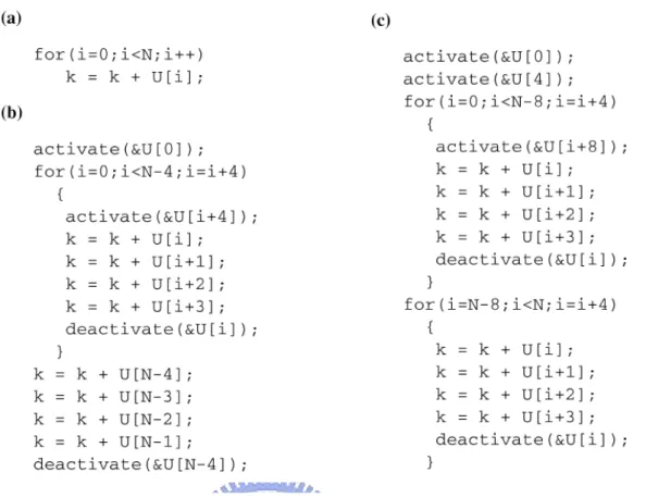
Let us focus on the code fragment in Figure 2-4a to illustrate this approach. In this code, a one-dimension array U is accessed sequentially with perfect spatial locality (suppose that k is stored in a register). Assuming that each line holds four array elements, Figure 2-4b shows the high-level code generated by this approach. In this transformed code, activate(&U[i+4]) preenergizes the next cache line (actually, the RCLs) to be accessed, whereas deactivate(&U[i]) deactivates the current cache line (actually, the RCLs) after its use. It should be noted that we implicitly assume that the time it takes to preactivate (preenergize) the next cache line is shorter than the time it takes to process the elements in the current cache line. In fact, one might even delay the activation of the next cache line further (e.g., just before the statement k = k + U[i+3] in Figure 1-5b), since it takes only 1 cycle to activate it. On the other hand, even if a particular leakage-control mechanism employed takes more time to effect, we can easily
accommodate it by inserting the activate instruction a bit earlier. Returning to the example in Figure 2-4a, let us assume an average cache line activation time of 8 cycles (for a hypothetical leakage-control) and a loop iteration of 4 cycles, we need to schedule the activate instructions two iterations ahead. This is illustrated in Figure 2-4c.
The compiler analysis needed to identify the program points to insert
activate/deactivate instructions involves a data reuse analysis. Specifically, the compiler needs to identify the array access patterns. Since trying to determine all loop iterations that reuse a given array element (or cache line) is costly, the implementation of W. Zhang et al. employs the data reuse framework given by Wolf and Lam [12]. This analysis tells us for each array reference what type of data reuse (temporal or spatial), if any, it exhibits. If a reference within the innermost loop exhibits temporal reuse, we insert the activate instruction just above the innermost loop, and insert the deactivate instruction after the innermost loop (i.e., the corresponding RCLs will be active only during the loop it is used). On the other hand, if the reference exhibits spatial reuse in the innermost loop, we first unroll the loop to make the references that access the same the same cache line explicit, insert the activate instruction ahead of time depending on the time it takes to activate cache lines (as in the example given in Figure 1-5), and insert the deactivate instruction only after all the references (in the loop body after the unrolling) that accesses the same cache line are touched. If, on the other hand, the reference in question does not exhibit any reuse in the innermost loop, we find the next (outer) loop level where it exhibits some form of reuse and insert the activate/deactivate instructions there.
2.2.3. A Preactivating Mechanism for a VT-CMOS Cache
performance degradation by preactivating cache lines using address prediction before access requests.
2.2.3.1. Power control scheme
Figure 2-5 shows the circuit of a line in the original DLC cache [9]. In DLC, each SRAM cell is composed of Variable-threshold CMOS (VT-CMOS) [14]. Any SRAM cells of any unselected lines are initially deactivated. In other words, the threshold voltages of transistors in a cell are high to suppress leakage current. When a reference address is applied and a line is selected after the address is decoded, all cells in the selected line are activated by changing the threshold voltages of transistors to a low voltage. This is done by the n-well and p-well drivers. Soon after being activated, the word line of the selected lines rises. Since the threshold voltages of the accessed cells are low, the delay of the bit line is as short as in a normal cache. Although the activated line consumes significant static power, it is negligibly small in a large cache. Note that the activation is triggered after the address is decoded and the activation time is
significant long (it is estimated in Section 2.2.2.3). As a result, the access time becomes
2.2.3.2. Leakage control policy
Figure 2-6 shows proposed processor organization (note that the figure does not present a precise pipeline organization; it depends on implementation). Although the organization is basically similar to the usual superscalar processor, it is differentiated by having an address predictor and a D-cache with three address inputs (reference, cancel, and reservation) per memory instruction. The address predictor predicts the address of a location which a memory instruction will access before the address is calculated. R. Fujioka et al. use a stride-based predictor to predict addresses because it gives the best cost/performance as an address predictor. The details of this predictor have been introduced in section 2.1.2.
Figure 2-7: Circuit of a line in the preactivating DLC cache Figure 2-6: Processor organization with a preactivating DLC cache
Figure 2-7 shows the organization of a line of our DLC cache. The differences from a conventional DLC cache are the two extra address decoders per memory
instruction, and an up/down counter we call the reservation counter per cache line. The counter indicates the number of the reservation for line accesses.
As shown in Figure 2-6, while instructions are decoded, the addresses of locations which will be accessed by decoding instructions are predicted using the address
predictor. The predicted addresses are written into an entry for the corresponding instruction in the instruction window. At the same time, they are sent to the D-cache as reservation addresses, and the reservation counter in each line is increased by one. If the counter value changes from zero to one, the corresponding line is activated to prepare for later actual references. When the counter value is non-zero, the line is continuously activated.
At some cycles later, a memory instruction is issued from the instruction window with the prior-written predicted address. An effective address is then calculated. The effective address is sent to the D-cache as a reference, and the predicted address as a cancel addresses. The reference address is used to access D-cache data in a usual cache. If the predicted address is correct, the selected cache line is already activated. Thus, delay due to DLC is not incurred; if not correct, a delay may be incurred. Meanwhile, the reservation counter in the selected line accessed by the cancel address is decreased by one. If the counter value becomes zero, the corresponding line is deactivated. Note that when a branch is found to be mispredicted, all reservation counters are reset.
2.2.3.3. Estimation of DLC cache delay
non-DLC cache for various capacities. Associativity for both caches are two (associativity has only a small impact according to the simulation, except for
direct-mapped). Two lines for each cache present the cases of 32B and 64B lines. As shown in Figure 1-9, the access time of a DLC cache is much larger than that of the non-DLC cache. As a line size becomes larger, the access time is longer. For example, the 32KB DLC cache with 32B or 64B lines has a 2.7or 3.9 times longer access time, respectively, than the non-DLC cache.
2.2.4. Summary and Observation
Table 1-3 summarizes the above three related works. As shown the “circuit technique” row in Table 1-3, drowsy cache, compared with DLC, has little wakeup latency. In addition, implementing a cache line is very few additions. The main
additions required to a standard cache line are a drowsy bit, a mechanism for controlling the voltage to the memory cells, and a word line gating circuit. Consequently, our cache architecture is based on drowsy cache.
Compiler approach has two disadvantages. First, program portability is restricted because it needs preprocessing. Second, it is only targeted to array-based applications, not to all applications. To avoid these two restrictions, propose a hardware preactivation mechanism applied for all applications based on drowsy data cache architecture is essential.
Although the third related work proposes a hardware preactivation mechanism, the address predictor overhead is too large (10KB SRAM). Our objective is to propose a hardware preactivation mechanism whose effectiveness is good and overhead is little.
Chapter 3 Proposed Design
In this chapter, we divide our design into three parts. First, we propose one data address prediction to predict the next data address sent by processor. Second, using our proposed data address prediction to preactivate oncoming accessed data cache line. Third, we introduce our de-activation policy for drowsy data cache.
3.1. Data address prediction
In this section, we will introduce our data address prediction. First, we introduce the basic idea of our prediction and list some design issues for this prediction. Then we show our block diagram of prediction hardware and our prediction mechanism and the implementation of data address prediction hardware.
3.1.1. Basic Idea of data address prediction
The goal of our data address prediction is to predict the next data address sent by processor. To achieve this goal, there are two works that we should do. First, we must have the ability to predict the next generated data address for one load/store instruction. Second, reserving each predicted data address in the order of instruction execution when each load/store instruction is executed. If we are able to do these two works, whenever executing the same instruction sequence, data address sent by processor would have high chance to be found in this prior reserved sequence. Thus the predicted next data address sent by processor is just it’s the data address next to founding data address.
However, there is one important problem is how to predict the next generated data address for one load/store instruction. The essence of this prediction relies on current data address and predicted stride value for this instruction. Noted that the term “stride value” means two prior consecutive data address for one load/store instruction. In this
paper, we take ARM ISA (instruction set architecture) as example. Because load/store instructions are implemented through base register plus offset addressing mode and base register plus index addressing mode and the percentage of former is much larger than latter (about 93% in MiBench). In base register plus offset addressing mode, this offset is invariable. Consequently, we divide load/store instructions into two types (auto-indexed and non auto-indexed) depending on base register behavior and decide its predicted stride value, respectively. For auto-indexed instruction type, which is often used to access array data, since the base register would be modified as original base register value plus offset after data access, so the next generated data address for this instruction type is predicted as the sum of current data address and offset field value (this offset value is our predicted “stride value” for this instruction type). For non auto-indexed instruction type, which is often used to access scalar data, since the base register would not be modified after its execution, so the next generated data address for this instruction type is predicted as the current data address (zero is our predicted stride value for this instruction type).
3.1.2. Design issue
There are two design issues before proposing our data address prediction. Issue 1 is about the size of table which is used to store predicted data address sequence. Since instruction execution has temporal locality, instructions that are executed recently are probably executed soon, we have not to reserve all predicted data addresses and just reserve recent predicted data addresses. Issue 2 is about how the predicted stride value is transferred. Since our goal in this paper is to reduce static power of data cache, the energy of additional hardware should not be too large. If one predicted stride value need to be completely transferred from processor to data cache, we should offer one
additional bus called stride bus and its length is equal to data bus. This cost is too large. Thus, our solution to this issue is collect the common predicted stride values, encode them, need one narrow bus (maybe 2-bit) to transfer them, and decode them in data cache.
3.1.3. Block Diagram of Data Address Prediction Hardware
Figure 3-1 shows the block diagram of data address prediction hardware. The additional components added to conventional drowsy data cache are a 4/2 encoder, 2 bit stride bus, 2/4 decoder, and DAST (Data Address Sequence Table) which is used to store predicted data address sequence. The four possible inputs for this encoder are our predicted stride value for load/store instructions, including three common offset values for auto-indexed load/store instructions and zero for non auto-indexed instructions. However, if its offset value for one auto-indexed instruction is not in these common offset values, we take zero as predicted stride value for this instruction. The output of encoder is sent to DAST through 2-bit stride bus. The value sent through stride bus is decoded by 2/4 decoder. DAST stores our predicted data address sequence. Each entry of DAST has two fields called PDA (predicted data address) and Stride. PDA stores the next generated data address for one load/store instruction, and Stride stores predicted stride value for one load/store instruction. DAST needs two pointers. One is called I_pointer which is used to indicate the insertion location when one predicted data address is stored into DAST. The other is called P_pointer which is used to indicate the location which predicted next data address sent by processor resides in.
3.1.4. Prediction mechanism
In this section, we describe our prediction algorithm in detail. First, we introduce when to predict data address and this is determined by DAST behavior. Second, we introduce how the predicted next data address sent by processor is generated. Third, we introduce how to maintain and update DAST.
3.1.4.1. DAST mode
Our prediction mechanism is implemented through DAST. DAST has two possible modes which decide its behavior when data address is sent to data cache. One is match mode, the other is verify mode. Figure 3-2 shows DAST mode transition diagram. When DAST is in match mode, data address sent to data cache would lookup DAST (fully search). If hitting, DAST changes to verify mode and one predicted data address is generated. This predicted data address means our predicted next data address sent by processor. When DAST is in verify mode, data address sent to data cache would check if it is the same as prior predicted data address. If yes, it means that our prior prediction is correct and another predicted next data address sent by processor is generated. If no, it means that our prior prediction is wrong, stopping prediction, and DAST returns to match mode.
3.1.4.2. How to predict the next data address sent by processor
In our data address prediction, the prediction time is when one data address could be found in reserved predicted data address sequence and the predicted next data address sent by processor is that address next to founding address in reserved sequence. Depending on DAST behavior, there are two cases for predicting the next used data address.
Case1: DAST is in match mode and lookup hit
In this case, it means one data address is found in the predicted data address sequence, so the predicted next used data address is the PDA field of the entry next to the hitting entry. Consequently, we pre-activate the corresponding data cache line.
PDA Stride
DA
P
DAST (match mode) hitting entry
As shown in Figure 3-3, the predicted next used data address is just as the PDA
Figure 3-2: DAST mode transition diagram
field indicated by P pointer.
Case2: DAST is in verify mode and predict correctly
In this case, it means we have predicted the current used data address. Consequently, we keep predicting the next used data address. The predicted next used data address is the PDA field of the entry next to the correct prediction entry. Consequently, we pre-activate the corresponding data cache line.
PDA Stride
P
DAST (verify mode) correct prediction entry DA
As shown in Figure 3-4, the predicted next used data address is just as the PDA field indicated by P pointer.
3.1.4.3. DAST maintenance
Depending on DAST behavior, we have three cases for updating DAST. For the sake of reserving predicted data address sequence, whatever the result of looking up DAST or predicting, we should do this action, delete one entry and insert one entry to the last of DAST.
Case 1: Lookup DAST hit or Correct prediction
When looking up DAST hit or predicting correctly, it means that we have the right stride value for this load/store instruction. Thus, fill the result of adding PDA field value
and Stride field value of current entry as well as Stride field value of current entry into the last entry of DAST. At the same time, we delete the current entry of DAST to reserved predicted data address sequence.
Case 2: Lookup DAST miss
When looking up DAST miss, it means that we have no information about the predicted data address of this instruction in DAST. Thus, fill the result of adding current data address in data address bus and the value in the stride bus as well as the value in the stride bus into the last of DAST.
Case 3: Wrong prediction
When wrong prediction occurs, it possibly means that we have the wrong predicted stride value for this load/store instruction. However, we could fix the right stride value through this wrong prediction. The right stride value should be: current data address sent by processor – the last generated data address of this load/store instruction. It is noted as: the last generated data address of this load/store instruction could be obtained from the wrong predicted data address and the wrong predicted stride value.
3.1.4.4. Handle multiple hit
When we use the current data address to index DAST, multiple hit may happen. This is because there are more than two instructions whose predicted data addresses are the same and the same data addresses are put into DAST. Figure 3-5 shows the original of multiple hit.
I DA
Hitting entry
Hitting entry
There are two solutions to multiple hit, called “top hit”, and “bottom hit”,
respectively. The appropriate situation using top hit: When one execution path would be executed continuously and there are more than two instructions whose predicted data addresses are the same. On the other hand, the appropriate situation using bottom hit: When one execution path would be executed continuously and there are no the same predicted data addresses for those instructions in this execution path.
These two solutions to multiple hit maybe not suitable solutions. However, after considering hardware cost, these solutions are candidates for handling multiple hit. In fact, we have another solution if we don’t consider hardware cost, and we call this solution is “best hit”. When there are more than two hitting entries, the PDA fields of next entry of hitting entries are all our predicted data address sent by processor. For instance, if entry 1 and entry 4 are hitting entries, the PDA fields of entry 2 and entry 5 are all our predicted data address sent by processor.
3.1.4.5. Handle wrong prediction
Before handing wrong prediction, we have to analyze and classify wrong prediction. We use one smart table to help us classify wrong prediction into “PC wrong” and “PDA wrong”. Figure 3-6 shows this smart table. Each entry of this table has three fields called PC, PDA, Stride. The operation of this table is similar to DAST. It is
now virtually analyze wrong prediction, so the assumption of sending PC to data cache is allowed.
PC PDA Stride
Smart table is indexed by data address just like DAST. When wrong prediction happens, we check if the PC field of this entry is the same as the current input PC. If it is not the same, we call this wrong prediction is PC wrong. If it is the same, we call this wrong prediction is PDA wrong. The cause of PC wrong may be changed instruction execution path, multiple hit, and etc. The cause of PDA wrong is due to wrong predicted data address for one load/store instruction.
Whatever the wrong prediction is PC wrong or PDA wrong, the handle of wrong prediction is not different. Recover the last generated data address, fix stride value, and calculate the predicted next generated data address. Obviously, this handle is aimed at PDA wrong. However, there is one problem is whether this handle is appropriate if wrong prediction is incurred by PC wrong. Our answer to this problem is yes if wrong prediction is incurred by changed instruction execution path. Our explanation is as follows. Figure 3-7 shows the different instruction execution path. If path 1 is executed consecutively and at one time path1 changes to path 2, there would be wrong prediction.
This is because the predicted data addresses on DAST are belonged to load/store instructions in path1, not path2. However, if path2 are also executed consecutively afterwards, we could predict the data address of load/store instructions in new path.
3.1.5. The flow chart and implementation for our data address
prediction
Figure 3-8 shows our flow chart of preactivation policy. In this figure, DA means the current data address sent by processor.
Figure 3-9 shows our implementation of data address prediction hardware. In this figure, lookup control is used to decide the search behavior (search all entries or just one entry) for the input address; write control is used to decide whether the output of
decoder is written into DAST or not; priority encoder is responsible for choosing one predicted data address when multiple hit happens.
state machine decoder DA PDA Stride priority encoder +/-+ + mux mux predicted data address I_pointer lookup control V P_pointer
3.2. Pre-activation policy
We use proposed data address prediction to preactivate oncoming data cache line. Figure 3-10 shows the implementation of preacitvation policy for drowsy data cache. To apply on pre-activation, we extra index decoder, n comparators (n: way numbers in data cache) to select the corresponding cache line.
tag index offset
V Tag Data V Tag Data
= = preactivate this line preactivate this line index decoder state machine decoder DA PDA Stride priority encoder +/-+ + mux mux I_pointer enco ded pr ed icted strid e value lookup control Mo di fied CA M V P_pointer w rite control
3.3. De-activation policy
Data cache access has locality property. In other words, the activity in data cache is only centered on a small subset of the lines during a fixed period of time. If we can put those unused cache lines into drowsy mode, we can reduce leakage energy of data cache. To implement this idea, we adopt the similar cache decay policy [8] proposed by
Kaxiras et al. A binary counter associates with each cache line. Whenever one cache line is accessed, its counter is reset to initial value (zero). The counter is incremented
periodically at fixed time intervals. If one counter saturates to its maximum value, this cache line switches to drowsy mode.
Chapter 4 Evaluation
In this section, we will show our simulation results. First, we will introduce our experiment methodology. Second, we give our evaluation metrics. Third, we show our experiment results.
4.1 Experiment methodology
To implement our proposed data address prediction, we used SimpelScalar/ARM. It allows detailed simulation of programs on a range of modern architectures using execution-driven simulation. Table 4-1 gives the default values of the parameters used in our base configuration. The energy values listed in the table are for 70nm technology. Note that leakage energy consumption is very critical in 70nm and below process technologies. Energy Parameters and drowsy transition time are obtained from [8] and [15].
Configuration Parameter Value Processor
Functional Units 4 Integer ALUs
1 integer multiplier/divider 4 FP ALUs
1 FP multiplier/divider
Decode/issue width 1 instruction/cycle
Commit width 1 instruction/cycle
In-order issue true
Cache and Memory hierarchy
L1 Instruction Cache 32 KB, 4 way, 32 byte blocks
L1 Data Cache 32 KB, 4 way, 32 byte blocks
Instruction TLB 16 entries, full-associative
Data TLB 16 entries, full -associative
L1 cache miss penalty 8 cycles
Branch Logic
Predictor bimodal (2-bit predictor)
BTB 128 sets, 4 way
Misprediction penalty 3 cycles
Energy Parameters
L1 dynamic energy per access 294 pJ
Leakage energy per cache line 0.417 pJ/cycle
Drowsy leakage energy per cache line 0.066304 pJ/cycle
Transition energy (low to high) 25.6 pJ/transition
Transition energy (high to low) 8.53 pJ/transition
Transition latency from drowsy mode 1 cycle
Transition latency from active mode 1 cycle
In order to evaluate the effectiveness of our methodology, we use MiBench to be our benchmark. It is a free, commercially representative embedded benchmark suite. MiBench consists of six categories including: Automotive and Industrial Control, Network, Security, Consumer Devices, Office Automation, and Telecommunications. The detail information about MiBench is in [16].
4.2 Evaluation metrics
First, we define ideal case for drowsy cache. This ideal case means that how many
4-1 shows our calculation for this ideal case. We could obtain that we would save the leakage energy of data cache if one cache line has not been used for 97 cycles.
off active drowsy mode_transition
mode_transition off
active drowsy
off
mode_transition
interval (leakage -leakage )=energy energy interval = leakage -leakage 25.6pJ+8.63pJ interval = 97 cycle 0.417pJ-0.066304pJ energy : e × ⇒ = active drowsy
nergy of power mode transition, including low to high and high to low leakage : leakage energy of active cache line per cycle
leakage : leakage energy of drowsy cache line per cycle
Next, we show our evaluation metrics. There are four metrics we would evaluate including: prediction coverage, prediction accuracy, energy saving, and performance loss.
number of prediction times 1. prediction coverage =
number of load/store instructions executed
number of correct prediction times 2. prediction accuracy =
number of total prediction times
SE Static energy consumption before applying preactivation
o
SE Static energy consumption after applying preactivation
n
3. Energy saving (SE - SE ) / SE 100% o n
SE active cycles active pow
o e o = = = × = × D D
E number of transitions transition e
overhead
r cycle time (k=total number of lines) 0 ~ k -1
drowsy cycles drowsy power
SE cycle time E
n active cycles active power overhead 0 ~ k -1 = × × ∑ × + ⎛ ⎞ = ∑ ⎜ ⎟× + × ⎝ ⎠ nergy
SP extra execution cycles cycle time E
system extraHW
E energy consumed by those HW needed by my preactivation policy
extraHW
+
× × +
=
CL*TP
4. performance loss = 100% ET
CL: cycle losses due to mode transition for total cache lines TP: transition penalty
ET: original exeuction time ×
4.3 Experiment results
In this section, we classify experiment results into prediction accuracy and leakage energy.
4.3.1 Prediction result
First, we want to know how many bits of stride bus are suitable. This needs to be analyzed from the common stride values for auto-indexed load/store instructions and the percentage of stride value=0 for non auto-indexed load/store instructions. Figure 4-2 shows the common offset value for auto-indexed load/store instructions. We would see that the percentage of offset value is equal to 1, 4, -4 is over 92% of total offset values.
offset percentage for auto-index instructions
0.720356107 0.179590453
0.052213513 0.047839927
offset=1 offset=4 offset=-4 others
Figure 4-3 shows the percentage of stride value=0 for non auto-indexed load/store instructions. We would see that the percentage of stride value=0 is about 50% for non auto-indexed load/store instructions.
stride value percentage for non auto-indexed instructions
0 0.1 0.2 0.3 0.4 0.5 0.6 0.7 0.8 0.9 1 stride=-32 stride=-8 stride=24 stride=13 stride=16 stride=3 stride=-3 stride=-1 stride=-2 stride=8 stride=-4 stride=1 stride=2 stride=4 stride=32 stride=0 Figure 4-3: stride value percentage for non auto-indexed load/store instructions
Then we collect the percentage of auto-indexed load/store instructions and non auto-indexed load/store instructions. Besides, we also collect the prediction accuracy if we take offset field value as its predicted stride value for auto-indexed load/store instructions and take 0 as its predicted stride value for non auto-indexed load/store instructions, and this collection we call data address behavior in Figure 4-4.
As shown in Figure 4-4, we see that the instruction percentage is 4:6 for
auto-indexed and non auto-indexed load/store instructions. Besides, the data address behavior is over 70% for auto-indexed load/store instructions, and over 50% for non auto-indexed load/store instructions.
0% 10% 20% 30% 40% 50% 60% 70% 80%
Auto-indexed Non Auto-indexed load/store instruction type
perc
enta
ge
instruction percentage data address behavior
0% 10% 20% 30% 40% 50% 60% 70%
size=8 size=16 size=32 size=64
DAST size
perc
en
tag
e
top hit bottom hit best hit
After analyzing the instructions of MiBench benchmark, now we evaluate the prediction accuracy for top hit, bottom hit, best hit From Figure 4-5, we could see that multiple hit seems have no effective solution because the accuracy of best hit is close top hit and bottom. From this figure, we could see top hit has better performance for our benchmark.
In this figure, best hit means that when multiple hit happens, we would use all multiple hit entries to predict the next data address sent by processor. Noted that the implementation of best hit is not practical, because its hardware cost would be larger than top hit and bottom hit.
Figure 4-6 shows the prediction coverage, accuracy, and multiple hit ratio of DAST. We see that DAST size=16 would have about 40% prediction coverage and about 55% prediction accuracy, and its multiple hit ratio is less than 5%. As the size of DAST increases, the gained performance is not obvious.
0.00% 10.00% 20.00% 30.00% 40.00% 50.00% 60.00% 70.00%
size=8 size=16 size=32 size=64 DAST size
pe
rce
nt
age
prediction coverage prediction accuracy multiple hit
Figure 4-7 shows that the performance for DAST and VHT. In this figure, DAST effect and VHT effect is calculated from DAST coverage * DAST accuracy and VHT coverage * VHT accuracy, respectively.
0% 10% 20% 30% 40% 50% 60% 70%
size=8 size=16 size=32 size=64 Table size pe rc en ta ge
DAST coverage VHT coverage DAST accuracy VHT accuracy DAST effect VHT effect
4.3.2 Leakage energy result
Figure 4-8 shows the leakage energy for the policies proposed in Section 2.2.1. We see that simple policy with 256 cycles decay interval and noaccess policy with 512 cycles decay interval have the best leakage energy reduction.
Compared with simple policy, noaccess policy has to add one counter for each cache line to monitor each cache line access. However, simple policy implementation just only needs one counter. Our simulation result shows that the benefit gained from simple policy would be better than noaccess policy.
20.00% 20.50% 21.00% 21.50% 22.00% 22.50% 23.00% 23.50%
DI=128 DI=256 DI=512 DI=1024 DI=2048 DI=4096
Decay Interval
Normalized Leakage Energy
simple policy noaccess policy
0% 5% 10% 15% 20% 25% 30%
size=8 size=16 size=32 size=64 size=128 size=256
VHT size
Normalized
Leakage Ener
gy
High_Leakage Low_Leakage Overhead
Figure 4-9 shows the leakage energy for the policy proposed in Section 2.2.3. In this figure, high leakage means that the energy which all cache lines consumed in active mode; low leakage means that the energy which all cache lines consumed in drowsy mode; overhead means the energy due to mode transition and extra hardware cost. We see that the VHT with 64 entries has the best leakage energy reduction. As table size increases, the energy consumed in overhead would be larger.
Figure 4-9 shows the leakage energy reduction for our proposed design. The bar named as “Line” and “Set” in this figure means the turn on/off unit: line or set. On the average, line is much better than set for leakage energy reduction. The X-axis means that how many entries DAST needs and how many cycles decay interval is. We see S16_I128 has the best leakage energy reduction, in other words, DAST size=16 entry with decay interval=128 cycles has the best leakage energy benefit.
Noted that 256 cycles, 512 cycles, 128 cycles are the best decay interval for simple policy, noaccess policy, DAST policy respectively. This means our policy put those unused cache lines into drowsy mode more aggressively than simple and noaccess policy. 15% 17% 19% 21% 23% 25% 27%
S8I64 S8I128 S8I256 S8I512 S8I1024 S8I2048 S16I64 S16I128 S16I256 S16I512 S16I1024 S16I2048 S32I64 S32I128 S32I256 S32I512 S32I1024 S32I2048 S64I64 S64I128 S64I256 S64I512 S64I1024 S64I2048
Size and decay interval
Normalized Leakage Energy
Line Set
![Figure 1-1: Trends in power across process technologies [1]](https://thumb-ap.123doks.com/thumbv2/9libinfo/8736082.203115/17.892.266.668.107.447/figure-trends-power-process-technologies.webp)
![Figure 2-5 shows the circuit of a line in the original DLC cache [9]. In DLC, each SRAM cell is composed of Variable-threshold CMOS (VT-CMOS) [14]](https://thumb-ap.123doks.com/thumbv2/9libinfo/8736082.203115/35.892.204.774.312.704/figure-circuit-original-composed-variable-threshold-cmos-cmos.webp)