Characterization of Si
ÕSiGe Heterostructures on Si Formed
by Solid Phase Reaction
C. H. Huang,a Albert Chin,a, zand W. J. Chenb a
Department of Electronics Engineering, National Chiao Tung University, Hsinchu, Taiwan
bDepartment of Materials Science and Engineering, National Huwei Institute of Technology, Huwei, Taiwan
We have characterized the Si/Si0.6Ge0.4 heterostructure formed by two-step solid-phase reaction. Single crystalline behavior is evidenced by X-ray diffraction. In sharp contrast to conventional strain-relaxed SiGe, an extremely smooth surface close to the Si substrate is measured by cross-sectional transmission electron microscopy and atomic force microscopy. Good material quality is further evidenced from the near identical current-voltage characteristics for thermal oxide grown on Si/Si0.6Ge0.4and on the Si control sample.
© 2002 The Electrochemical Society. 关DOI: 10.1149/1.1450618兴 All rights reserved.
Manuscript submitted June 4, 2001; revised manuscript received October 23, 2001. Available electronically February 7, 2002.
Although silicon-germanium共SiGe兲 heterostructures1-11 on sili-con 共Si兲 have been studied extensively, one difficult challenge to integration of strained SiGe into current Si complementary metal-oxide-semiconductor field-effect transistor共CMOSFET兲 processes is the low temperature (T⬍ 800°C)12required to avoid strain relax-ation and defect generrelax-ation. This is because SiGe is generally grown by a low pressure chemical vapor deposition共LPCVD兲 at low tem-perature but current CMOS process must use a high tempera-ture annealing for dopant activation after source-drain ion implantation.12Unfortunately, strain will be relaxed at high tempera-tures and may degrade the device performance by forming rough surface and pinholes.4-8In addition to low dopant activation, the low temperature restriction for strained SiGe also degrades gate oxide integrity, increases source-drain junction leakage, and is incompat-ible to modern high dielectric constant gate dielectrics.13-14 There-fore, strain-relaxed SiGe has attracted much attention recently, but the strain relaxation related rough surface still prohibits further ap-plication of SiGe to current Si CMOS technology.9-11Recently, we have developed a strain-relaxed SiGe using a new high temperature solid phase reaction method; good integrity of p-MOSFET is obtained.15-16In this paper, we have characterized the Si/SiGe het-erostructures on Si substrate by two-step solid-phase reaction. Good material quality is revealed by X-ray diffraction共XRD兲 and cross-sectional transmission electron microscopy 共XTEM兲. The primary advantage of this simple method is the full compatibility to the existing Si ultralarge-scale integration 共ULSI兲 technology without the constraint of low temperature processing or alternating the per-formance of Si CMOS devices.
Experimental
Standard Si wafers of 10⍀ cm resistivity were used in this study. After a standard RCA clean, HF vapor passivation is used to sup-press the native oxide formation before Ge deposition.14-18An amor-phous Ge layer of 120 Å is selectively deposited by lithography in active region to form a single crystalline Si0.3Ge0.7layer15by rapid
thermal annealing共RTA兲 at 900°C for 60 s. More detailed material characterization can be found in our previous study.15Then Si/SiGe heterostructure is formed by a 150 or 300 Å amorphous Si deposi-tion and subsequent RTA, while the thicker Si is used for material analysis and the thinner one is for device characterization.
MOS capacitors were fabricated by growing a 30 Å thermal ox-ide at 900°C, a 3000 Å poly-Si deposition, phosphorus doping, Al metallization, and patterning. XRD, cross-sectional TEM, secondary ion-mass spectroscopy 共SIMS兲, capacitor leakage current, and capacitance-voltage 共C-V兲 measurements are used to characterize the material property Si/SiGe heterostructure.
Results and Discussion
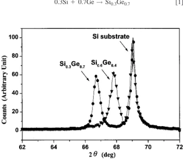
Figure 1 shows the XRD spectra of one-step formed Si0.3Ge0.7
and two-step formed Si/SiGe heterostructure by solid-phase reac-tion. The comparable sharp and strong XRD peaks for Si0.3Ge0.7and
Si0.6Ge0.4with Si substrate indicates a single crystalline and high
quality Si0.6Ge0.4, where the single crystalline Si0.3Ge0.7 is
previ-ously demonstrated.15A Ge composition of 0.4 was obtained in Si/SiGe heterostructure from the relative XRD peak position to Si substrate. The composition change from Si0.3Ge0.7to Si/Si0.6Ge0.4
may be due to additional Si supplied from top Si layer that dilutes the Ge content.
We have used XTEM to further characterize the top Si layer of the Si/Si0.6Ge0.4heterostructure. As shown in Fig. 2, two uniform
layers are observed on Si substrate and form the Si/Si0.6Ge0.4
het-erostructure. No polycrystalline grain can be observed in XTEM that is consistent with the narrow and sharp XRD peak shown in Fig. 1. Good material quality is evidenced by the smooth surface, smooth interface, and almost defect free Si/Si0.6Ge0.4 heterostructure. In
combination of smaller thickness of Si top layer with Ge composi-tion decreasing after solid-phase reaccomposi-tion, the mechanism of second-step reaction is due to the intermixing of top Si with underneath SiGe. Further, TEM, shows that the formed Si0.6Ge0.4and the
re-maining top Si layers are⬃300 and ⬃160 Å that are in close agree-ment with the calculated data from the following reaction equations 0.3Si⫹ 0.7Ge → Si0.3Ge0.7 关1兴
zE-mail: achin@cc.nctu.edu.tw
Figure 1. XRD spectra of one-step formed Si0.3Ge0.7and two-step formed
Si/Si0.6Ge0.4heterostructure by solid-phase reaction.
Journal of The Electrochemical Society, 149共3兲 G209-G211 共2002兲
0013-4651/2002/149共3兲/G209/3/$7.00 © The Electrochemical Society, Inc.
G209
) unless CC License in place (see abstract).
ecsdl.org/site/terms_use
address. Redistribution subject to ECS terms of use (see
140.113.38.11
0.43Si⫹ 0.57Si0.3Ge0.7→ Si0.6Ge0.4 关2兴
According to Eq. 1, a 120 Å deposited Ge will form a 170 Å Si0.3Ge0.7. From Eq. 2, the Si0.3Ge0.7in turn gives a 300 Å Si0.6Ge0.4
and a remaining top 170 Å Si layer. The good agreement between calculated and transmission electron microscopy共TEM兲 measured data again suggests that the top Si layer is the main source of Si for Si0.6Ge0.4. This is reasonable because the top amorphous Si layer
has weaker bonding than bottom single crystalline Si or Si0.3Ge0.7
layers.
We have further measured the composition profile of Si/Si0.6Ge0.4
heterostructure. As shown in Fig. 3, a uniform composition of SiGe measured by SIMS is consistent with the sharp XRD peak in Fig. 1. A thin Si layer at top surface with very low Ge is also observed that suggests the composition transition from Si0.3Ge0.7 to Si/Si0.6Ge0.4
originated from top Si. The long graded Ge composition tail adja-cent to uniform Si0.6Ge0.4may be due to Ge diffusion into Si
sub-strate. Because the graded Ge profile is naturally formed during the solid-phase reaction, it is important for strain relaxation of the uni-form Si0.6Ge0.4layer and achieving a smooth Si/Si0.6Ge0.4interface
in Fig. 2.
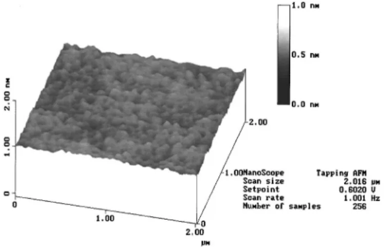
Because the device performance of the MOSFET is directly re-lated to the surface roughness before and after oxidation,14,18 we have used atomic force microscopy共AFM兲 to further measure the surface roughness of Si/SiGe heterostructure. The top Si layer cal-culated from above equations is about 20 Å. As shown in Fig. 4, a root-mean-square共rms兲 value of 1.5 Å is measured that is close to the original Si surface value of 1.2 Å. The small rms roughness is
also consistent with the smooth surface observed by TEM. To our best knowledge, this is the smoothest surface of strain relaxed Si/ SiGe that can be used for further device application.
We have further characterized the Si/Si0.6Ge0.4heterostructure by
measuring the capacitor leakage current. As shown in Fig. 5, almost identical I-V characteristics are obtained for 30 Å thermal oxides grown on both Si/Si0.6Ge0.4and Si that suggests the excellent quality
of oxide grown on Si/Si0.6Ge0.4 heterostructure. The comparable
electrical characteristics with Si control sample is because the ther-mal oxide is grown on top Si instead of on SiGe that avoids the weak GeOx inside the SiO2matrix.1-2
The quality of oxide grown on Si/Si0.6Ge0.4 heterostructure is
further examined by the C-V characteristics. Figures 6a and b show the measured high and low frequency C-V curves and interface trap density (Dit) plot, respectively. The Ditas a function of energy is
obtained directly from measured C-V data. The close match between high and low frequency capacitance values indicates the high oxide quality with low bulk and interface defects. This is further evidenced from the low minimum interface trap density of 6
⫻ 1010 eV⫺1/cm2, which is already good enough for MOSFET
applications.14
Conclusions
We have demonstrated a simple method to fabricate Si/SiGe het-erostructure with good material quality, which is fully compatible
Figure 2. Cross-sectional TEM of the Si/Si0.6Ge0.4heterostructure.
Figure 3. SIMS profile of the Si/Si0.6Ge0.4heterostructure.
Figure 4. AFM surface topography of the Si/Si0.6Ge0.4heterostructure.
Figure 5. I-V characteristics of 30 Å thermal oxide grown on Si and Si/Si0.6Ge0.4.
Journal of The Electrochemical Society, 149共3兲 G209-G211 共2002兲
G210
) unless CC License in place (see abstract).
ecsdl.org/site/terms_use
address. Redistribution subject to ECS terms of use (see
140.113.38.11
to the existing Si CMOS technology. The excellent oxide quality grown on Si/SiGe is evidenced from the almost identical oxide
leak-age current with control thermal SiO2, which can be further used for
p-MOSFET application.
Acknowledgments
The authors would like to thank Professor K. C. Hsieh at the Department of Electrical Engineering, University of Illinois. The work was supported by NSC共89-2215-E-009-099兲 of Taiwan.
National Chiao Tung University assisted in meeting the publication costs of this article.
References
1. D. K. Nayak, K. Kamjoo, J. S. Park, J. C. S. Woo, and K. L. Wang, Appl. Phys.
Lett., 57, 369共1990兲.
2. H. K. Kiou, P. Mei, U. Gennser, and E. S. Yang, Appl. Phys. Lett., 59, 1200共1991兲. 3. P. W. Li, E. S. Yang, Y. F. Yang, J. O. Chu, and B. S. Meyson, IEEE Electron
Device Lett., 15, 402共1994兲.
4. S. Verdonckt-Vandebroek, E. F. Crabbe, B. S. Meyerson, D. L. Harame, P. J. Restle, J. M. C. Stork, and J. B. Johnson, IEEE Trans. Electron Devices, 41, 90共1994兲. 5. R. S. Prassad, T. J. Thornton, S. Kanjanachuchai, J. Fernandez, and A. Matsumura,
Electron. Lett., 31, 1876共1995兲.
6. G. Ternent, A. Asenov, I. G. Thayne, D. S. MacIntyre, S. Thoms, C. D. W. Wilkin-son, E. H. C. Parker, and A. M. Gundlach, Electron. Lett., 35, 430共1999兲. 7. P. K. Swain, S. Madapur, and D. Misra, Appl. Phys. Lett., 74, 3173共1999兲. 8. T. E. Jackman, J. M. Baribeau, and D. J. Lockwood, Phys. Rev. B, 45, 13591
共1992兲.
9. J. L. Liu, C. D. Moore, G. D. U’Ren, Y. H. Luo, Y. Lu, G. Jin, S. G. Thomas, M. S. Goorsky, and K. L. Wang, Appl. Phys. Lett., 75, 1586共1999兲.
10. T. Bryskiewicz, Appl. Phys. Lett., 66, 1237共1995兲.
11. A. Sakai, T. Tatsumi, and K. Aoyama, Appl. Phys. Lett., 71, 3510共1997兲. 12. Y. Taur and T. K. Ning, Fundamental Modern VLSI Devices, p. 286, Cambridge
University Press, New York共1998兲.
13. S. C. Song, H. F. Luan, C. H. Lee, A. Y. Mao, S. J. Lee, J. Gelpey, S. Marcus, and D. L. Kwong, in Proceedings of the Symposium on VLSI Technology, IEEE, p. 137
共June 1999兲.
14. A. Chin C. C. Liao, C. H. Lu, W. J. Chen, and C. Tsai, in Proceedings of the
Symposium on VLSI Technology, IEEE, p. 135共June 1999兲.
15. Y. H. Wu, W. J. Chen, A. Chin, and C. Tsai, Appl. Phys. Lett., 74, 528共1999兲. 16. Y. H. Wu, A. Chin, and C. Tsai, IEEE Electron Device Lett., 21, 350共1999兲. 17. Y. H. Wu, W. J. Chen, S. L. Chang, A. Chin, S. Gwo, and C. Tsai, IEEE Electron
Device Lett., 20, 200共1999兲.
18. A. Chin, B. C. Lin, W. J. Chen, Y. B. Lin, and C. Tsai, IEEE Electron Device Lett.,
19, 426共1998兲.
Figure 6.共a, top兲 C-V characteristics and 共b, bottom兲 interface trap density plot of 30 Å thermal oxide grown on Si and Si/Si0.6Ge0.4.
Journal of The Electrochemical Society, 149共3兲 G209-G211 共2002兲 G211
) unless CC License in place (see abstract).
ecsdl.org/site/terms_use
address. Redistribution subject to ECS terms of use (see
140.113.38.11