Conductivity and tunneling density of states in granular Cr films
Yu-Chen Sun,1Sheng-Shiuan Yeh,2 and Juhn-Jong Lin1,2,*
1Department of Electrophysics, National Chiao Tung University, Hsinchu 30010, Taiwan 2Institute of Physics, National Chiao Tung University, Hsinchu 30010, Taiwan 共Received 12 April 2010; revised manuscript received 14 July 2010; published 12 August 2010兲 We have measured the tunneling differential conductances, G共V兲, of four Al/AlOx/Cr planar tunnel junc-tions as well as the conductivities,共T兲, of the Cr electrodes at liquid-helium temperatures. The Cr electrodes were made to be granular with dimensionless intergrain tunneling conductance spanning from g⯝1 to gⰇ1, and the dimensionality of the granular array d = 3. For the samples with gⰇ1, we found that the measured G共V兲 curves display large zero-bias singularities which obey a ln V law at low bias voltages共ⱗ a few millielectron volt兲 while crossing over to a
冑
V law at high bias voltages. Simultaneously, the conductivities of the Cr electrodes reveal ln T dependence below a characteristic temperature. These results are explained in terms of the recent theory of granular metals. In a sample with g⯝1, in addition to the conductivity dependence ⬀ln T, we observed a universal scaling behavior of the normalized differential conductance 关G共V,T兲 − G共0,T兲兴/冑
T with the combined parameter冑
e兩V兩/kBT in a wide temperature interval of 2.5–32 K. This result is not yet understood.DOI:10.1103/PhysRevB.82.054203 PACS number共s兲: 73.20.⫺r, 73.40.Gk, 73.40.Rw, 72.80.Ng I. INTRODUCTION
Granular conductors, which are composite materials of metallic granules and dielectric components, have recently attracted much renewed theoretical attention as tunable sys-tems for addressing mesoscopic physics problems.1,2In con-trast to disordered “homogeneous systems,” the electronic-transport properties of granular conductors are largely governed by the strength of the intergrain tunneling.1 Theo-retically, a granular conductor is characterized by a number of physical quantities: the mean energy-level spacing in a single granule, ␦, the dimensionless tunneling conductance between neighboring granules, g 共i.e., the average tunneling conductance between neighboring grains expressed in units of 2e2/h兲, and the single-grain Coulomb charging energy, Ec.
For strong intergrain coupling共gⰇ1兲 and in the not-too-low temperature interval g␦ⰆkBTⰆEc 共where kB is the
Boltz-mann constant兲, charging effects are important yet the quantum-interference weak-localization 共WL兲 effects are suppressed. This unique regime provides a tempting oppor-tunity to probe the electronic conduction properties due to the many-body Coulomb interaction effects in the presence of granularity. The electrical conductivity is predicted to obey the law,2,3
共T兲 =0
冋
1 − 1 2gdln冉
gEc kBT冊
册
, 共1兲where d is the dimensionality of the granular array and 0 = 2共e2/h兲ga2−dis the classical conductivity without the Cou-lomb interaction 共i.e., the system conductivity at tempera-tures kBTⰇEc兲, and a is the radius of the 共spherical兲 grain. It
is important to note that, unlike that due to the WL and electron-electron interaction 共EEI兲 effects in weakly disor-dered homogeneous systems,4this⬀ln T law in Eq. 共1兲 is predicted to hold for all dimensions since the dimensionality
d only enters the prefactor of the logarithmic correction term.
On contrary, the functional form of the tunneling electronic density of states 共DOS兲 is predicted to depend critically on
sample dimensionality. For d = 3 共which is pertinent to the present experiment兲,2,3 3共⑀兲 =0
冋
1 − A 4gln冉
gEc max共kBT,⑀兲冊
册
, 共2兲where⑀is the tunneling electron energy measured from the Fermi level EF, 0 is the DOS in the absence of Coulomb interaction, and A is a numerical prefactor. The underlying physics which leads to the conductivity and DOS corrections given in Eqs.共1兲 and 共2兲, respectively, is due to the presence of local voltage fluctuations between neighboring granules.
Experimentally, it is intriguing that electrical-transport measurements on systems with strong intergrain coupling of-ten revealed ln T dependence of resistivity,5,6rather than of conductivity.7,8 Therefore, the prediction of Eq. 共1兲 still awaits convincing experimental test. Moreover, there is still no experimental observation in three-dimensional 共3D兲 granular films concerning the electronic DOS predicted by Eq. 共2兲. In the opposite limit of weak intergrain coupling 共gⰆ1兲, the conductivity at low temperatures is theoretically and experimentally established to possess the Efros-Shklovskii-type dependence, i.e.,共T兲⬀exp共−
冑
T0/T兲, where T0is a characteristic temperature.5,7,9–11In this work, we have studied four Al/AlOx/Cr planar
tunnel junctions comprising of granular Cr electrodes with intergrain tunneling conductance spanning from g⯝1 to g Ⰷ1. Moreover, the dimensionality of the granular arrays 共the Cr electrodes兲 was made to have d=3, insofar as the electronic-transport properties are concerned. Our measured conductivities of the Cr electrodes obey the ⬀ln T law, as predicted by Eq. 共1兲. Furthermore, our measured tunneling DOS reveals the ln⑀ law, as predicted by Eq. 共2兲. These results not only verified the recent theory of granular metals1,2,12 but also clarified the nonmagnetic nature of the “giant” zero-bias conductance dips previously found in many Cr composed tunnel junctions.13,14 We mention in passing that, previously, the Efros-Shklovskii-type temperature de-pendence had been found in our nanocontacts formed with
granular Cr films, where the ⬀exp共−
冑
T0/T兲 behavior wasobserved in the broad temperature interval of 1–100 K.15 In that case, we experimentally realized the regime gⰆ1.16
This paper is organized as follows. In Sec.II, we discuss our experimental consideration and method for sample fab-rication of granular Cr electrodes and Al/AlOx/Cr tunnel
junctions as well as our measurement procedure. Section III contains our experimental results and discussion. We inter-pret our measured conductivity and tunneling DOS in terms of the theory of granular metals, and rule out the WL and EEI effects developed for weakly disordered homogeneous conductors to be the origins of our observations. Our conclu-sion is presented in Sec.IV
II. EXPERIMENTAL METHOD
The reason for selecting Cr as our electrode material is because Cr films deposited in a vacuum often form granular, rather than uniform and continuous, layers.15,17,18 For ex-ample, a 10-nm-thick Cr film deposited by thermal evapora-tion on a mica substrate showed a distribuevapora-tion of disk-shaped granules with a diameter of⬃ a few tens of nanometer and a height of ⬇2–6 nm, as was evidenced from atomic force microscopy 共AFM兲 studies.15 Varying the deposition rate modified the average grain size.17Even thermally evaporated in a vacuum having a background pressure as low as ⬃1 ⫻10−6 mbar, the surfaces of Cr granules became oxidized and formed thin dielectric layers of CrOx.18In this work, we
carried out our thermal evaporation deposition at a pressure
of ⬃5⫻10−6 mbar so that our films were guaranteed to form metallic Cr granules separated by thin CrOx dielectric
layers.
To study the conductivity and the tunneling DOS of granular Cr films, we fabricated four Al/AlOx/Cr planar
tun-nel junctions by using the standard thermal evaporation method as described previously.19A set of parallel, relatively clean 0.8 or 1 mm wide and 25 nm thick Al films were first deposited on glass substrates held at room temperature. The surfaces of the as-deposited Al films were subsequently oxi-dized by utilizing plasma discharge to produce a ⬇1.5–2 nm-thick AlOx layer. A long Cr electrode 共1 mm
wide, and 15–30 nm thick兲 was then deposited across the parallel AlOxcoated Al strips to complete the tunnel junction
geometries. At the same time, the Cr electrode was attached with leads appropriate for four-probe electrical measure-ments关see Fig.1共a兲for a schematic diagram兴. The resistivi-ties of our Al reference electrodes were typically 13共16兲 ⍀ cm at 4 共300兲 K, corresponding to the product
kFᐉ⬇54 at 4 K, where kFis the Fermi wavenumber andᐉ is
the electron mean free path. The conductivity of the Cr elec-trode in each set of junctions was adjusted by varying the mean Cr film thickness and the deposition rate between 0.01 and 1.5 nm/s. To achieve a very low conductivity in the junction D, the Cr film was deposited onto a cold substrate held at liquid-nitrogen temperature, by employing a very low deposition rate of ⬃0.01 nm/s. The tunneling differential conductances, G共V,T兲=dI共V,T兲/dV, across the junctions were measured by utilizing the standard lock-in technique, where I is the tunneling current between the Al and Cr elec-trodes, and V is the voltage dropped across the insulating barrier关see Fig.1共b兲for a schematic diagram兴.19Before per-forming any detailed measurements of G共V,T兲 curves, we checked to ensure the high quality of each tunnel junction by measuring the superconducting gap of the clean Al electrode at 0.25 K. 共Our Al electrodes became superconducting at ⬇1.8–2 K.兲 Table Ilists the values for the relevant param-eters of the four Cr electrodes comprising the tunnel junc-tions A–D studied in this work.
III. RESULTS AND DISCUSSION
A. Temperature dependence of conductivity and differential conductance curves
Figure 2共a兲shows the variation in normalized resistivity,
共T兲/共280 K兲, with temperature for the four Cr electrodes FIG. 1. 共Color online兲 Diagrams depicting 共a兲 four-probe
resis-tance measurements of Cr electrodes and共b兲 differential conduc-tance measurements of Al/AlOx/Cr tunnel junctions. Black strips
stand for Al films, and green共gray兲 strips for Cr electrodes.
TABLE I. Values for relevant parameters of the Cr electrodes in Al/AlOx/Cr tunnel junctions. AJ is the junction area and RJ is the junction resistance at 300 K. t is the thickness, 共R䊐兲 is the resistivity 共sheet resistance兲 at 2.5 K, and NCr,d共0兲 is the DOS at the Fermi energy. kFᐉ was calculated by using the Drude model. The diffusion constant D was evaluated through the Einstein relation −1 = NCr,d共0兲e2D. The values of kFᐉ and D were evaluated for 2.5 K. Ec,0, g, and a are defined in Eq.共1兲. Notice that the values of a are only
listed for reference because our Cr granules are disk-shaped rather than spherical.
Sample AJ 共mm2兲 RJ 共k⍀兲 t 共nm兲 共⍀ cm兲 R䊐 共⍀兲 NCr,d共0兲 共J−1m−3兲 k Fᐉ D 共cm2/s兲 Ec 共meV兲 共⍀−10cm−1兲 g a 共nm兲 A 0.8⫻1.0 1.0 30 115 38.3 2.4⫻1047 5.1 1.4 5 8690 62 5.5 B 0.8⫻1.0 4.5 25 154 61.6 1.8⫻1047 4.1 1.4 7 6560 42 5.0 C 1.0⫻1.0 11 15 290 193 1.1⫻1047 2.6 1.3 4 3500 10 2.2 D 0.8⫻1.0 4.0 25 5060 2024 2.8⫻1046 0.23 0.28 22 260 0.96 2.8
of our tunnel junctions. Except for the junction A, the resis-tivities of all other samples monotonically increase with de-creasing temperature. However, the amounts of the resistivity rise are much smaller than what would be expected for samples falling deep on the insulating side, where resistivity should show ⬀exp共
冑
T0/T兲 dependence and rapidly in-crease with decreasing temperature. This result immediately reflects that the intergrain tunneling conductances g in our Cr electrodes must be large. In particular, a ln T dependence of the conductivity was found in all Cr electrodes at liquid-helium temperatures. Figures 2共b兲 and2共c兲show that the ⬀ln T law holds for more than one decade of temperature in the junctions B and D, respectively. Correspondingly, the normalized differential conductances, G共V兲/G共70 mV兲, of these tunnel junctions reveal essentially symmetric dips cen-tered at zero-bias voltage, Fig. 3. It is clearly seen that the differential conductance dips are markedly more pronounced in junctions comprised of more disordered Cr electrodes. Therelative changes in G共V兲 at 2.5 K are 关G共0兲
− G共70 mV兲兴/G共70 mV兲=−0.27, −0.36 and −0.89 in the junctions A, C and D, respectively. These magnitudes of rela-tive change in G共V兲 are more than one order of magnitude larger than what would be expected from the EEI effect in weakly disordered homogeneous conductors.4
We have measured the differential conductance curves in external magnetic fields applied perpendicular to the junction plane. The left共right兲 inset of Fig.3shows the G共V兲 curves of the junction A共D兲 in zero magnetic field 共symbols兲 and in a magnetic field of 4 T共solid curve兲. These two insets firmly demonstrate that the magnetic field caused a negligible change 共ⱗ0.05%兲 in G共V兲. A negligible magnetic field ef-fect, together with the strong dependence of the magnitudes of G共V兲 dips on the level of disorder displayed in the main panel of Fig. 3, strongly suggests that our observed large conductance dips must be associated with some sort of dis-order effect in the granular Cr electrodes. In other words, any magnetic origins, which have long been suspected to play an important role in Cr comprised junctions, can be ruled out.13,14
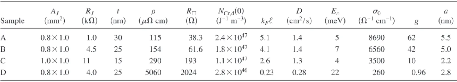
Figure4共a兲shows the normalized G共V兲/G共10 mV兲 spec-tra of our Al/AlOx/Cr junctions at 2.5 K in the positive bias
voltage regime.关Recall that our G共V兲 curves are essentially symmetric around the zero-bias voltage.兴 Specifically, we found that in the junctions A–C, G共V兲/G共10 mV兲⬀ln V for
Vⱗ10 mV, and it crosses over to the G共V兲/G共10 mV兲
⬀
冑
V law at higher bias voltages, Fig. 4共b兲. On the other hand, in the junction D, the G共V兲/G共10 mV兲⬀冑
V law wasobeyed from relatively low bias voltages all the way up to a notably high bias voltage of⬃100 mV, see the inset of Fig. 4共b兲.
B. Comparison with theoretical predictions
In this subsection, we compare our experimental results with available theoretical predictions concerning disordered
10 180 210 240 0 100 200 300 0.9 1.0 1.1 1.2 1.3 1.4 1.5 1.6 T (K) T (K) D (b) 2 4 6 8 20 40 6480 6500 6520 1 10 (a) B A B C D ρ (T) / ρ (280 K) (c) σ ( Ω -1 cm -1 )
FIG. 2. 共Color online兲 共a兲 Normalized resistivity, 共T兲/共280 K兲, as a function of temperature of the Cr electrodes in junctions A-D, as indicated. Conductivity as a function of tempera-ture of the Cr electrodes in共b兲 junction B and 共c兲 junction D. The straight solid lines are least-squares fits to Eq.共1兲.
-90 -60 -30 0 30 60 90 0.0 0.2 0.4 0.6 0.8 1.0 -10 -5 0 5 10 20 40 60 80 -10 -5 0 5 10 390 405 420 D D A A C G (V) /G (70 mV) V (mV) G( µ S ) V (mV) G (µ S) V (mV)
FIG. 3. 共Color online兲 Normalized differential conductance, G共V兲/G共70 mV兲, as a function of bias voltage for junctions A, C, and D, as indicated. Notice that the G共V兲 curves are essentially symmetric around zero-bias voltage. Insets: The left 共right兲 inset shows the G共V兲 curve of junction A 共D兲 in zero magnetic field 共symbols兲 and in a perpendicular magnetic field of 4 T 共solid curve兲. Notice that the magnetic field causes a negligible change. Data were taken at 2.5 K. 1 10 1.0 1.2 1.4 1.6 1.8 0 2 4 6 8 10 1.0 1.5 0 5 10 0 1 2 3 D (b) (a) G (V )/ G (10 mV ) V (mV) D C B A V1/2(mV1/2) G (V) /G (10 mV) C A V1/2 (mV1/2 ) G (V)/ G (1 0 m V)
FIG. 4. 共Color online兲 共a兲 Normalized differential conductance, G共V兲/G共10 mV兲, as a function of bias voltage for junctions A–D, as indicated. The straight solid lines are least-squares fits to Eq.共2兲.
For clarity, the data for the junctions B, C, and D have been verti-cally shifted up by 0.1, 0.2, and 0.8, respectively. 共b兲 G共V兲/G共10 mV兲 versus
冑
V for junctions A, C, and D, as indicated. The straight solid lines are guide to the eyes. Data were taken at 2.5 K.conductors. We first explain that our results cannot be de-scribed by the conventional EEI effect originally developed for weakly disordered homogeneous conductors by Altshuler and co-workers.4,20,21 共The WL effects are even less impor-tant, because, on one hand, the electron dephasing length is short in granular samples22 and, on the other hand, our Cr electrodes are magnetic.23兲 Then, we discuss our observa-tions in terms of the recent theory of granular metals formu-lated by Efetov and Tschersich2 and Beloborodov and co-workers.1,3
1. Ruling out the weak-localization and electron-electron interaction effects
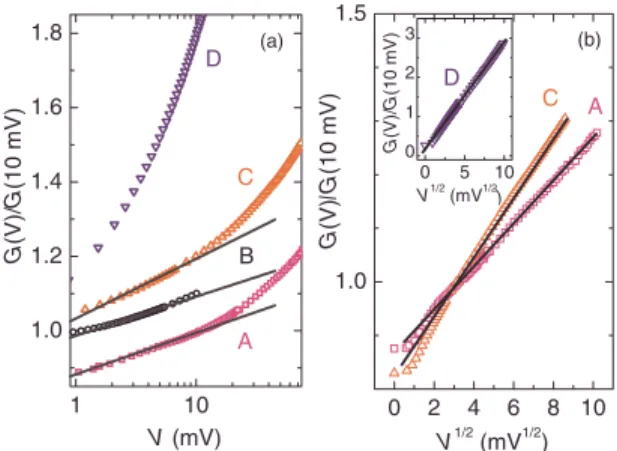
In order to understand our G共V兲 results in a quantitative manner, we first determine the parabolic background tunnel-ing conductance共PBTC兲 in our junctions.24It is known that a PBTC is characteristic of every metal-insulator-metal tun-nel junction at high bias voltages, where the disorder induced suppression in DOS, regardless of its origin, is insignificant.2,4 Figure 5 shows the G共V兲 curves in a wide range of V for the junctions A and D. It is seen that G共V兲 ⬀V2 共the solid curves兲 in the wide interval of 兩V兩 ⬇200–400 mV. This observation confirms that our mea-sured zero-bias conductance dips are superimposed on a PBTC. From this fitted PBTC, we can extrapolate the zero-bias conductance, Gpara共0兲, of an as would be ideal Al/AlOx/Cr tunnel junction consisting of a “clean” Cr
elec-trode. The extrapolated value of Gpara共0兲 contains the infor-mation about the DOS at EFin a clean Cr electrode, because
for small bias voltages and at low temperatures, Gpara共0兲 can be approximated by Gpara共0兲= PNAl共0兲NCr,c共0兲, where P is the electron tunneling rate 共which depends on the barrier height and width兲, and NAl共0兲 and NCr,c共0兲 are the DOS at EF
in the Al and clean Cr electrodes, respectively.25The DOS at EFin our granular and disordered Cr electrode, NCr,d共0兲, can
then be evaluated through the relation NCr,d共0兲=NCr,c共0兲 ⫻关G共0兲/Gpara共0兲兴, where the measured zero-bias
conduc-tance G共0兲= PNAl共0兲NCr,d共0兲. With the literature value of
NCr,c共0兲=3.5⫻1047 J−1m−3 in clean Cr metal,26 our ex-tracted magnitudes of NCr,d共0兲 are listed in TableI.
For two-dimensional 共2D兲 weakly disordered homoge-neous conductors, Altshuler and co-workers4,20 have pre-dicted that the EEI effect causes a minute suppression in the DOS around zero-bias voltage
␦N2共⑀兲 N2共0兲 =2 e2R䊐 82បln
冋
⑀ បD冉
t 2冊
2册
, 共3兲where N2共0兲 is the measured DOS at EF,2 is the
electron-electron coupling constant in 2D, R䊐is the sheet resistance,
D is the electron diffusion constant, and t is the sample
thick-ness. The tunneling electron energy⑀is measured relative to
EF. For a given film thickness, as兩V兩 increases, the effective
dimensionality of the EEI effect will cross over from 2D to 3D at兩V兩ⲏVc⬇共42បD兲/共et2兲.27 In 3D, the EEI correction
to the DOS is given by4,21
␦N3共⑀兲 N3共0兲 =
3
冑
⑀4
冑
22共បD兲3/2N3共0兲, 共4兲where N3共0兲 is the measured DOS at EF, and 3 is the
electron-electron coupling constant in 3D.
At first glance, since our junctions A and B are nominally weakly disordered 共kFᐉ⬇4–5兲, one might attempt to
at-tribute our G共V兲⬀ln V results to the 2D EEI effect. However, such an interpretation can be ruled out as follows. By com-paring our measured ln V dependence of G共V兲 in the junction A with the prediction of Eq. 共3兲, we obtained a value 2 ⬇448. This value is one order of magnitude larger than the theoretical prediction of 2= ln关共បD4t2兲/共42⑀兲兴⬇43, where =共me2kFt兲/共22ប20兲, and 0 is the permittivity of
the vacuum4共we took a typical electron energy ⑀= 5 meV兲. Furthermore, in the high bias voltage regime, a comparison of our measured G共V兲⬀
冑
V result with Eq. 共4兲 yielded a value of3⬇88, which is also far higher than the theoretical prediction of 3⬇2.4 Therefore, our observed giant G共V兲 dips cannot be due to the EEI effect in weakly disordered homogeneous conductors. Definitely, the granularity in the structure of our Cr electrodes must play an important role,15,17,18as to be addressed below.2. Logarithmic temperature dependence of conductivity
Let us discuss that our results can be satisfactorily, but not fully, interpreted in terms of the recent theory of granular metals. We have fitted our measured⬀ln T results with Eq. 共1兲. To carry out the least-squares fits, we assume a value of the charging energy Ec⬇10kBTⴱ, where Tⴱis the temperature
below which the⬀ln T law holds. Taking this value of Ec
and the sample dimensionality d = 3共because our Cr granules are disk-shaped with a height of ⬇0.5–2.5 nm, which is much smaller than our mean film thickness of 15–30 nm兲, we have extracted the values of the parameters0and g in our samples共see TableI兲. It should be noted that the extracted0 and g values are insensitive to the choice of Ec value,
be-cause Ecappears in the argument of a logarithmic function.28
Inspection of TableIindicates that in the junctions A–C we obtained gⰇ1. This result is in good consistency with the
-400 -200 0 200 400 600 750 900 1050 1200 1350 -300 0 300 0 300 600 900 A G ( µ S) V (mV) D V (mV) G( µ S )
FIG. 5. 共Color online兲 G共V兲 spectra of junctions A and D at 2.5 K in a wide bias voltage interval, as indicated. The symbols are the experimental data and the solid curves are parabolic fits. The solid curves in junctions A and D are described by Gpara共V兲=848 + 0.067V + 0.0028V2 and Gpara共V兲=272−0.12V+0.0026V2, respec-tively, where Gparais in microsiemens and V in millivolt.
prerequisite for Eq.共1兲 to be applicable. On the other hand, our extracted value of g⯝1 in the junction D implies that this sample falls marginally inside the regime of validity of Eq. 共1兲. We notice that Eq. 共1兲 was formulated by consider-ing a periodic cubic array of uniformly sized grains and ne-glecting dispersion of the intergrain tunneling conductance,1 while our samples contained random arrays of varying-sized, disk-shaped granules.15 Therefore, a close quantitative com-parison of our 共and other groups’8,29,30兲 experiment with theory is not possible at this stage.
Another important feature of the predictions of the theory of granular metals is that Eq. 共1兲 should be valid at any magnetic field. This is indeed confirmed by our experiment. We have measured共T兲 of the Cr electrode in the junction A between 2 and 20 K in both zero magnetic field and in a perpendicular magnetic field of 4 T. The measured values are the same to within our experimental uncertainty. On contrary, the WL effect, if any exists, should be very sensitive to and suppressed by even a small magnetic field.23If the EEI effect were responsible, we should then have observed a
冑
T, butnot a ln T, dependence in this sample in this temperature interval.31Therefore, both the WL and EEI effects are irrel-evant to our observations in Figs.2共a兲–2共c兲.
The mean energy level spacing␦ in our Cr granules may be evaluated as follows. We have carried out AFM studies of a film deposited under conditions similar to those used for the fabrication of the junction B. We found that the Cr film formed a granular structure consisting of disk-shaped grains of ⬇60⫾20 nm in diameter and ⬇1.5⫾1 nm in height, along with a few larger aggregations. By taking an average diameter of⬃60 nm and an average height of ⬃1.5 nm, we obtain an estimate of ␦= 1/NCr,d共0兲V¯⬇2 eV, where V¯ is the average granule volume. This␦ value in turn suggests a characteristic temperature TB⬇g␦/kB⬇1 K above which
Eq.共1兲 is expected to apply. Experimentally, the⬀ln T law in our junction B is observed in the temperature interval 0.3–7 K, see Fig.2共b兲. This degree of agreement is satisfac-tory, considering that the evaluations of parameters in a granular sample unavoidably involve large uncertainties.
Using our estimated values of EC⬇6 meV 共see TableI兲
and ␦⬇2 eV, we obtained the ratio Ec/␦⬇3⫻103. This
ratio suggests the existence of a broad range for logarithmic corrections to conductivity. However, even under such cir-cumstances, Feigel’man et al. have theoretically shown that a simple ⬀ln T law should still hold in a wide range of temperature.32 This prediction is confirmed by the present experiment.
3. Differential conductance curves and tunneling density of states
Tuning to the differential conductance curves, we discuss the crossover behavior of G共V兲 from the ln V to
冑
Vdepen-dence. This occurs at a characteristic bias voltage of Vc
⬇Ec/e⬇10kBTⴱ/e. Theoretically, the application of Eq. 共2兲
requires the condition max共T,⑀兲ⱗEcto be satisfied. That is,
at low temperatures such that kBT⬍⑀, the3共⑀兲⬀ln⑀law is
predicted for the regime⑀ⱗEc. On the other hand, the
varia-tion in 3 with⑀in the opposite limit共⑀ⲏEc兲 has not been
calculated. Experimentally, in the junctions A–C, we
ob-served G共V兲⬀ln V in the low bias voltage regime 共VⱗVc
⬇Ec/e⬇a few to ⬃10 mV兲. This is qualitatively in line
with the prediction of Eq.共2兲. However, a close comparison with theory cannot be made at this stage because the numeri-cal prefactor A in Eq. 共2兲 was calculated for the case when the logarithmic term is much smaller than 1.2Quantitatively, the magnitudes of the G共V兲 dips we observed are much larger than that predicted by Eq.共2兲. On the other hand, our
g values are larger than the critical intergrain tunneling
con-ductance gC=共2d兲−1ln共Ec/␦兲 共⬇0.4, using the above Ec/␦
value兲.3Therefore, we do not expect to find a “hard” gap in our samples.12Our G共V兲⬀
冑
V results in the high bias voltage regime 共VⲏVc兲 also have to await a future theoreticalexplanation.33
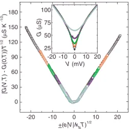
Finally, in the junction D, we did not observe any G共V兲 ⬀ln V dependence even at relatively low bias voltages, which may be due to the fact that g⯝1 in this sample and thus Eq. 共2兲 is marginally applicable. 关However, recall that we found the ⬀ln T behavior, as predicted by Eq. 共1兲.兴 In fact, G共V兲⬀
冑
V was observed in this sample in a wide rangeof 兩V兩⬇1–100 mV at 2.5 K, Fig. 4共b兲. Furthermore, we found that in this particular sample, the scaled differential conductance关G共V,T兲−G共0,T兲兴/
冑
T versus the combinedpa-rameter
冑
e兩V兩/kBT for different measurement temperaturesbetween 2.5 and 32 K collapse closely onto a single curve, Fig. 6. This result strongly suggests the existence of a uni-versal scaling function in the g⯝1 regime. That is, there exists a function f such that G共V,T兲−G共0,T兲=
冑
T⫻ f共
冑
eV/kBT兲, where f should depend on the combinedpa-rameter
冑
eV/kBT, instead of depending independently on eVor kBT. For comparison, the inset of Fig. 6 shows the
un-scaled G共V兲 versus bias voltage V at five measurement tem-peratures. Previously, a universal scaling behavior of differ-ential conductance has been theoretically predicted for 3D weakly disordered homogeneous conductors 共Refs. 21 and 27兲. Our observation of Fig.6 demonstrates that a universal scaling phenomenon also exists in the granular case. This
-20 -10 0 10 20 -20 -10 0 10 20 25 50 75 100 0 30 60 90 120 150 180 G ( µ S) V (mV) [G (V ,T )-G (0, T )]/ T 1/2 ( µ SK -1 /2 ) +(e|V|/kBT)1/2
FIG. 6. 共Color online兲 Normalized differential conductance, 关G共V,T兲−G共0,T兲兴/
冑
T, as a function of the combined parameter冑
e兩V兩/kBT for the junction D at five measurement temperatures. Notice that the data points collapse closely. Inset: unscaled G共V兲 versus bias voltage V at共from bottom up兲 2.5, 5.0, 9.0, 16, and 32 K.issue deserves further theoretical investigations.
IV. CONCLUSION
We have measured the conductivities共T兲 in granular Cr electrodes and the differential conductances G共V兲 in Al/AlOx/Cr tunnel junctions at liquid-helium temperatures.
In samples with dimensionless intergrain tunneling conduc-tances gⰇ1, we found⬀ln T and G共V兲⬀ln V at low bias voltages. These results are satisfactorily understood in light of the recent theory of granular metals. A crossover of G共V兲 from the ln V to
冑
V dependence was observed at high biasvoltages. In a sample with g⯝1, we found ⬀ln T and
G共V兲⬀
冑
V in a wide bias voltage interval. Moreover, thenor-malized differential conductance 关G共V,T兲−G共0,T兲兴/
冑
Tre-veals a universal scaling behavior with the combined
param-eter
冑
e兩V兩/kBT in a wide range of temperature. This lastobservation requires a further theoretical explanation. Fi-nally, we would like also to note that, while the theory of granular metals considers a periodic array of uniformly sized grains, in real samples one often has some distribution in granule size. The effect of such size distribution on our re-sults in the present study has yet to be fully addressed.
ACKNOWLEDGMENTS
The authors are grateful to Zhi-Qing Li and Shao-Pin Chiu for valuable assistance at the early stage of the experi-ment. This work was support by the Taiwan National Science Council through Grants No. NSC 97-2112-M-009-017-MY2 and No. NSC 98-2120-M-009-004, and by the MOE ATU Program. Y.C.S. was partly supported by the NCTU-RIKEN Joint Graduate School Program.
*jjlin@mail.nctu.edu.tw
1I. S. Beloborodov, A. V. Lopatin, V. M. Vinokur, and K. B. Efetov,Rev. Mod. Phys. 79, 469共2007兲.
2K. B. Efetov and A. Tschersich, Phys. Rev. B 67, 174205
共2003兲;Europhys. Lett. 59, 114共2002兲.
3I. S. Beloborodov, K. B. Efetov, A. V. Lopatin, and V. M. Vi-nokur,Phys. Rev. Lett. 91, 246801共2003兲.
4B. L. Altshuler and A. G. Aronov, in Electron-Electron Interac-tions in Disordered Systems, edited by A. L. Efros and M. Pollak 共North-Holland, Amsterdam, 1985兲.
5R. W. Simon, B. J. Dalrymple, D. Van Vechten, W. W. Fuller, and S. A. Wolf,Phys. Rev. B 36, 1962共1987兲.
6A. Gerber,J. Phys.: Condens. Matter 2, 8161共1990兲.
7A. Gerber, A. Milner, G. Deutscher, M. Karpovsky, and A. Gladkikh,Phys. Rev. Lett. 78, 4277共1997兲.
8L. Rotkina, S. Oh, J. N. Eckstein, and S. V. Rotkin,Phys. Rev. B 72, 233407共2005兲.
9B. Abeles, P. Sheng, M. D. Coutts, and Y. Arie,Adv. Phys. 24,
407共1975兲.
10T. B. Tran, I. Beloborodov, X. M. Lin, T. P. Bigioni, V. M. Vinokur, and H. M. Jaeger,Phys. Rev. Lett. 95, 076806共2005兲.
11I. S. Beloborodov, A. V. Lopatin, and V. M. Vinokur,Phys. Rev.
B 72, 125121共2005兲.
12I. S. Beloborodov, A. V. Lopatin, G. Schwiete, and V. M. Vi-nokur,Phys. Rev. B 70, 073404共2004兲.
13J. M. Rowell and L. Y. L. Shen,Phys. Rev. Lett. 17, 15共1966兲. 14F. Mezei and A. Zawadowski,Phys. Rev. B 3, 3127共1971兲. 15Y. H. Lin, Y. C. Sun, W. B. Jian, H. M. Chang, Y. S. Huang, and
J. J. Lin,Nanotechnology 19, 045711共2008兲.
16It should be aware that the ⬀−exp共
冑
T0/T兲 dependence can alternatively and satisfactorily be explained by the conductivity theory of P. Sheng, B. Abeles, and Y. Arie,Phys. Rev. Lett. 31, 44共1973兲. Further experiments to critically discriminate the mi-croscopic origins of this temperature behavior in the insulating regime would be highly meaningful.17P. A. Gould,Br. J. Appl. Phys. 16, 1481共1965兲.
18V. A. Krupenin, V. O. Zalunin, and A. B. Zorin,Microelectron.
Eng. 81, 217共2005兲.
19S. S. Yeh and J. J. Lin,Phys. Rev. B 79, 012411共2009兲. 20B. L. Altshuler, A. G. Aronov, and A. Yu. Zyuzin, Zh. Eksp.
Teor. Fiz. 86, 709共1984兲 关Sov. Phys. JETP 59, 415 共1984兲兴. 21B. L. Altshuler and A. G. Aronov,Solid State Commun. 30, 115
共1979兲.
22X. X. Zhang, C. Wan, H. Liu, Z. Q. Li, P. Sheng, and J. J. Lin,
Phys. Rev. Lett. 86, 5562共2001兲.
23J. J. Lin and J. P. Bird, J. Phys.: Condens. Matter 14, R501
共2002兲.
24W. F. Brinkman, R. C. Dynes, and J. M. Rowell,J. Appl. Phys. 41, 1915共1970兲.
25E. L. Wolf, Principles of Electron Tunneling Spectroscopy 共Ox-ford University Press, New York, 1985兲.
26I. Estermann, S. A. Friedberg, and J. E. Goldman,Phys. Rev. 87,
582共1952兲.
27Y. Imry and Z. Ovadyahu,Phys. Rev. Lett. 49, 841共1982兲. 28Alternatively, for spherical grains of radius a separated by
insu-lating barriers with average thickness s, the charging energy is predicted to be Ec= 2se2/r0a共a/2+s兲, where 0is the
permit-tivity of vacuum andris the dielectric constant of the
insulat-ing barrier 共Refs. 9and 16兲. Taking r⬇13 for Cr2O3 关P. H. Fang and W. S. Brower,Phys. Rev. 129, 1561共1963兲兴, a thick-ness s⬃0.2 nm, and a diameter a⬃10 nm, we obtain an esti-mate of Ec⬃10 meV. This estimated value is in good accord
with those values obtained by using Ec⬇10 kBTⴱ.
29M. Huth, D. Klingenberger, Ch. Grimm, F. Porrati, and R. Sach-ser,New J. Phys. 11, 033032共2009兲.
30P. Achatz, W. Gajewski, E. Bustarret, C. Marcenat, R. Piquerel, C. Chapelier, T. Dubouchet, O. A. Williams, K. Haenen, J. A. Garrido, and M. Stutzmann, Phys. Rev. B 79, 201203共R兲, 共2009兲.
31Using D = 1.4 cm2/s, we obtain the thermal diffusion length LT=
冑
Dប/kBT⬇33/冑
T nm in the sample A. Therefore, in termsof the EEI effect, the Cr electrode should be 3D at temperatures above ⬇1 K. If we insisted in plotting resistance versus tem-perature for the sample B共D兲, a dependence R⬀ln T is observed
in essentially the same temperature interval shown in Fig.2共b兲
关Fig.2共c兲兴. However, the measured resistance rise is more than a
factor of 3 as could be expected from the 2D EEI and WL effects, taking the sheet resistance listed in TableIinto calcula-tion.
32M. V. Feigel’man, A. S. Ioselevich, and M. A. Skvortsov,Phys.
Rev. Lett. 93, 136403共2004兲.
33Previously, a G共V兲⬀