fect was designed to modulate the 60 and 120 photonic crystal (PC) bend corners and Y-branch PC power splitters. In the pre-liminary experiments, the average bend losses of 60 and 120 PC bend waveguides for both polarizations were lower than 1.5 and 4.2 dB/bend, respectively. For the Y-branch PC power splitters, power imbalances for both polarizations were all lower than 0.7 dB. It shows that the fabricated Si-based ARROW-B PCWs can provide good light sharp-bend ability and power-split ability.
Index Terms—Antiresonant reflecting optical waveguide (ARROW), bend waveguide, photonic crystal (PC), photonic crystal waveguide (PCW), power splitter.
I. INTRODUCTION
P
HOTONIC CRYSTALS (PCs) are periodic structures for dielectric constants. If line defects are introduced into two-dimensional (2-D) PCs to construct 2-D PC waveg-uides (PCWs), certain frequency ranges of lightwaves can propagate well in PCs by photonic band gaps (PBGs) [1], [2]. The well-designed PCWs can provide good light transmis-sion through sharp-bend and Y-branch structures. It can be further applied for the development of ultracompact photonic integrated circuits (PICs). To increase the light transmission through the bend corner, many possible methods have been proposed, such as adjusting the positions of air holes [3]–[7], changing the radius of certain air holes at the bend corner [7],Manuscript received October 31, 2011; revised April 24, 2012; accepted April 24, 2012. Date of publication May 03, 2012; date of current version June 06, 2012. This work was supported in part by the National Nano Device Labora-tories for device fabrication and in part by the National Science Council of the Republic of China under Grant NSC 99-2120-M-009-004.
J.-H. Chen is with the Department of Electronics Engineering and Institute of Electronics, National Chiao Tung University, Hsinchu 30010, Taiwan (e-mail: hackerking.ee94g@nctu.edu.tw).
Y.-T. Huang is with the Department of Electronics Engineering and Insti-tute of Electronics, and the Department of Biological Science and Technology, National Chiao Tung University, Hsinchu 30010, Taiwan (e-mail: huangyt@cc. nctu.edu.tw).
Y.-L. Yang is with the Advanced Transistor Research Division, Taiwan Semiconductor Manufacturing Company, Ltd., Hsinchu 30077, Taiwan (e-mail: ylyang.ee93g@nctu.edu.tw).
M.-F. Lu is with the Department of Electronics Engineering, Minghsin Uni-versity of Science and Technology, Hsinfeng, Hsinchu 304, Taiwan (e-mail: mflu@must.edu.tw).
Color versions of one or more of the figures in this paper are available online at http://ieeexplore.ieee.org.
Digital Object Identifier 10.1109/JLT.2012.2197671
Although these methods can greatly increase the high-transmis-sion bandwidth and efficiency, complicated time-consuming computation and modulation are often needed [9]. For the fabrication process, it is also a challenge to pattern and etch out such specific shapes as the original design [15]. Any fabrication shifts could affect the overall transmission bandwidth and efficiency.
In our research, we used a simple capsule-shaped design to modulate 60 and 120 PC bend corners, and Y-branch PC power splitters by directly connecting two adjacent air holes with a rectangular-shaped defect [11], [17]–[19]. Compared with the conventional topology design, the capsule-shaped defect has a relatively large defect size and a smooth hole shape. For the lithography and etching processes, it becomes much easier to maintain hole shapes as the original design. Besides, we combined a PCW with a type-B antiresonant reflecting optical waveguide (ARROW-B) [20] instead of an index-guiding structure in the vertical direction to improve the coupling efficiency with a single-mode fiber. ARROW-B structures have been proposed as optical chip platforms because of some attractive advantages: 1) a relatively large core size with quasi single-mode propagation for efficient coupling with a single-mode fiber [21]; 2) a relatively lower core refractive index than a conventional waveguide for the use of a high sensi-tive evanescent-field-type refractometric sensor [22] or surface plasmon resonance biosensor [23]; 3) a low-loss leaky-guiding mechanism for the realization of a directional coupler with a short coupling length [24]; 4) easy fabrication and flexible material choices and thickness control for each layer [25]. In this paper, we will show the design, fabrication, and charac-terization of Si-based ARROW-B PC bend waveguides and Y-branch power splitters applied at the optical communication wavelength m for the TE-like and TM-like modes.
II. DESIGN OF ANARROW-B SLABWAVEGUIDE
A basic ARROW-B slab waveguide consists of three layers: a core layer with a refractive index and thickness , a first cladding layer with a low refractive index and thickness , and a second cladding layer with a high refractive index and thickness , respectively. Two cladding thicknesses must be chosen appropriately to satisfy low-loss and quasi single-mode propagation. The first cladding thickness is so thin such that the frustrated total internal reflection occurs at the interface of the
2346 JOURNAL OF LIGHTWAVE TECHNOLOGY, VOL. 30, NO. 14, JULY 15, 2012
Fig. 1. Propagation losses in an ARROW-B waveguide as functions of the first cladding thickness for first four (a) TE modes and (b) TM modes.
core and the first cladding layer. The second cladding thickness is chosen by the antiresonant condition [25]:
(1) If the refractive index of the core layer is equal to that of the second cladding layer, (1) can be further reduced to
(2) Although increasing the thickness of the core layer is benefi-cial for butt coupling with a single-mode fiber, it has a challenge for the deep-etching process [18], [19]. To consider the fabrica-tion feasibility and provide a good light-coupling support, we chose the thicknesses and refractive indices of the core layer and the second cladding layer as m,
m, and , respectively. The refractive index of the first cladding layer was chosen as . To choose an appropriate thickness of for the quasi single-mode propa-gation, the propagation losses of the first four TE and TM modes as functions of the thickness in an ARROW-B slab wave-guide were calculated with the transfer matrix method [26], which are shown in Fig. 1(a) and (b), respectively. As we chose m, the propagation losses of the fundamental TE and TM modes were lower than 1 dB/cm, and those of higher order TE and TM modes were much higher than 10 dB/cm. Thus, ef-fective single-mode propagation could be attained.
To verify the coupling efficiency from a single-mode fiber to a 7- m-width ridged ARROW-B structure or a 7- m-width ridged silicon-on-insulator-based (SOI-based) waveguide, we performed three-dimensional finite-difference time-domain (3-D FDTD) simulations to calculate the overlap integrals between the fiber mode and the ridged-waveguide modes at the connected interface. The single-mode fiber has a core diam-eter of 6 m with a refractive index of 1.451 and a cladding diameter of 125 m with a refractive index of 1.445. The
ridged SOI-based waveguide has a core thickness of 0.22 m with a refractive index of 3.5 and a cladding thickness of 2.0 m with a refractive index of 1.46. The calculated coupling efficiency between the single-mode fiber and the 7- m-width ridged SOI-based waveguide was only 18.5%. However, the calculated coupling efficiency between the single-mode fiber and the 7- m-width ridged ARROW-B structure was 59.2%. It shows a significant coupling improvement due to a relatively large core size of an ARROW-B structure.
III. DESIGN OF ARROW-B 60 AND120 PC BENDWAVEGUIDES
Air holes arranged in a triangular lattice were used to con-struct a 2-D PC con-structure for a broad TE band gap [3]. The ra-dius of holes was set as 0.4 for the largest PBG, where was the lattice constant. The 2-D photonic band structure was cal-culated by the 2-D plane-wave expansion method. As shown in Fig. 2, there was only a TE band gap ranging from 0.4 to 0.5 . We chose m and m so that the operation frequency could fall in the band gap region. One row of air holes in the -K direction was removed to construct a 2-D PC bend waveguide.
We introduced a capsule-shaped design [17], [18] into our 60 PC bend waveguide, as shown in Fig. 3(a). The capsule-shaped defect consisted of two air holes directly linked by a rectan-gular-shaped defect with a length . To have the output channel to be parallel to the input channel, the double 60 bend corners were used. The capsule-shaped design is much easier than the conventional topography design because we only di-rectly connect two adjacent air holes at the bend corner without any complicated computation to make a modulation of hole shapes. The 2-D FDTD simulations for observing the TE mode profiles through the conventional and designed 60 PC bend waveguides are shown in Fig. 3(b) and (c), respectively. As seen in Fig. 3(b), the effective channel width at the bend corner was a little broader than a straight PCW width, so the field through a conventional 60 PC bend corner easily excited an odd mode. Since the mode was different from the original even
Fig. 2. TE/TM band structures in a 2-D PC.
Fig. 3. (a) Schematic of a designed 60 PC bend waveguide and the path of the light transmission. (b) Steady-state field distributions by the 2-D FDTD simula-tion through the convensimula-tional 60 PC bend waveguide. (c) Mode profile through the designed 60 PC bend waveguide.
mode guiding in the input PCW, the mode mismatch would cause large light reflection and scattering. In Fig. 3(c), the field through the designed capsule-shaped bend corner could be re-garded as propagating in a short-width bend waveguide sur-round two air claddings [18]. Similar designs and characteri-zations have also been confirmed experimentally by some re-searchers [11], [17]. The light could be well confined with the help of index-like guiding and photonic-bandgap guiding.
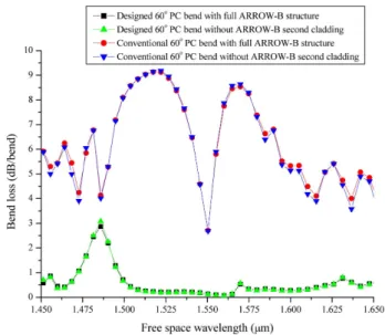
Combining the 60 PC bend with the ARROW-B structure, we then performed the 3-D FDTD simulations of bend losses in four types of the 60 PC bends to verify which transmission optimization is mainly contributed from the capsule-shaped de-sign or the ARROW-B structure. As shown in Fig. 4, it is found that the improvement of light transmission at the 60 PC bend is mainly contributed from the capsule-shaped design rather than the ARROW-B structure. For the wavelength ranging from 1.50 to 1.62 m covering the C-band and L-band frequency ranges, the bend loss of our designed 60 PC bend waveguide was lower than 0.5 dB/bend. It shows that our designed 60 PC bend wave-guide can be integrated into the PICs and be applied for both C-band and L-band optical communications.
Fig. 4. Bend loss spectra of TE-like modes in four types of the 60 PC bends by the 3-D FDTD simulation.
Fig. 5. (a) Schematic of a designed 120 PC bend waveguide and the path of the light transmission. (b) Steady-state field distributions by the 2-D FDTD simulation through the conventional 120 PC bend waveguide. (c) Mode profile through the designed 120 PC bend waveguide.
We further extended the mirror-like idea of the 60 PC bend design into the 120 PC bend waveguide, as shown in Fig. 5(a). Without any calculation or modulation of the hole position at the sharp-bend corner, we used a sharp-bend design consisting of three air holes directly linked by two rectangular-shaped defects with the same length . The 2-D FDTD simulations for observing the TE-mode profiles through the conventional and designed 120 PC bend waveguides are shown in Fig. 5(b) and (c), respectively. In Fig. 5(b), it is clearly seen that the con-ventional 120 PC bend corner looks like a small cavity [27], so the field through the bend corner would excite a cavity mode, unlike the original even mode guiding in the input PCW. Such structure and mode mismatch caused the light to reflect and scatter at the bend corner. By introducing two capsule-shaped defects into the 120 bend corner, as shown in Fig. 5(c), the two capsule-shaped defects could act as two mirror-like struc-tures and support sharp-bend propagation without any transient cavity-mode exciting.
Combining the 120 PC bend with the ARROW-B structure, we also performed the 3-D FDTD simulations of bend losses in four types of the 120 PC bends to verify which transmission
op-2348 JOURNAL OF LIGHTWAVE TECHNOLOGY, VOL. 30, NO. 14, JULY 15, 2012
Fig. 6. Bend loss spectra of TE-like modes in four types of the 120 PC bends by the 3-D FDTD simulation.
Fig. 7. (a) Schematic of a designed Y-branch PC power splitter and the path of the light transmission. (b) Steady-state field distributions by the 2-D FDTD simulation through the conventional Y-branch PC power splitter. (c) Mode pro-file through the designed Y-branch PC power splitter.
timization is mainly contributed from the capsule-shaped design or the ARROW-B structure. As shown in Fig. 6, it is found that the improvement of light transmission at the 120 PC bend is mainly contributed from the capsule-shaped design rather than the ARROW-B structure. For the wavelength ranging from 1.50 to 1.58 m covering the C-band frequency ranges, the bend loss of our designed 120 PC bend waveguide was lower than 1 dB/bend. It shows that our designed 120 PC bend waveguide can be integrated into the PICs and be applied for the C-band optical communications.
IV. DESIGN OF AN ARROW-B Y-BRANCH
PC POWERSPLITTER
For improving the power-split efficiency in a Y-branch PCW, one air hole at the Y-junction region was replaced by a capsule-shaped defect [11], [19]. This defect consisted of two air holes linked by a rectangular line defect with a length , as shown in Fig. 7(a). To prevent the interfield coupling of two output channels, output channels were set parallel to the input channel with the same capsule-shaped 60 bend corner and were separated with a distance.
Fig. 8. Transmission spectra of TE-like modes in four types of the Y-branch PC power splitters at one output channel by the 3-D FDTD simulation.
Fig. 7(b) and (c) shows the 2-D FDTD simulations for observing the TE-mode profiles through the conventional and designed capsule-shaped Y-junction regions, respectively. In Fig. 7(b), the effective channel width at the conventional Y-junction region was very broad, so the higher-order modes might be excited. Owing to the structure discontinuity and mode mismatch at the Y-junction region, much light was reflected. As shown in Fig. 7(c), the designed capsule-shaped defect at the Y-junction region could reduce two channel widths at the Y-junction region and eliminate the higher order mode excitation and the field reflection [19].
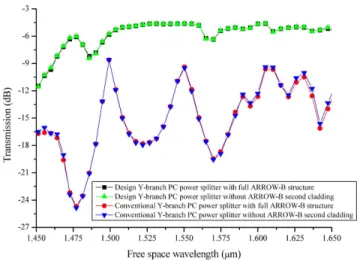
Combining the Y-branch PC power splitter with the ARROW-B structure, we performed the 3-D FDTD simu-lations to get the transmission spectra of one channel output for TE-like modes in four types of the Y-branch PC power splitters to verify which transmission optimization is mainly contributed from the capsule-shaped design or the ARROW-B structure. As shown in Fig. 8, it is found that the improvement of light transmission at the Y-branch PC power splitter is mainly contributed from the capsule-shaped design rather than the ARROW-B structure. For the wavelength ranging from 1.50 to 1.56 m covering the C-band frequency ranges, our designed PC Y-branch power splitter provided transmission for one output channel higher than dB. The total transmission of two output channels was higher than dB. It shows that our designed Y-branch PC power splitter can be integrated into the PICs and be applied for the C-band optical communications.
V. SCHEMATICLAYOUT OF THEARROW-B PC BEND
WAVEGUIDE ANDPOWERSPLITTER
The schematic layout for analyzing the efficiencies of the ARROW-B PC bend waveguides and power splitters is shown in Fig. 9. It consists of a straight PCW, 60 and 120 PC bend waveguides, and a Y-branch PC power splitter. For 60 and 120 PC bend waveguides, two kinds of lateral shift distances with 12.8 and 25.6 m were designed to verify the bend ability. All PC bend losses were normalized to a straight PCW with the same propagation length. For the Y-branch PC power splitter, two kinds of separation distances with 25.6 and 51.2 m were designed to verify the power-split ability. Two lateral tapered
Fig. 9. Schematic of a Si-based ARROW-B: (a) straight PCW, (b) 60 and (c) 120 PC bend waveguides, and (d) a Y-branch PC power splitter.
Fig. 10. AEI images. (a) to (f) are top-view images and (g) to (h) are cross-sectional view images. (a) Straight PCW. (b) 60 PC bend waveguide. (c) 120 PC bend waveguide. (d) Y-branch PC power splitter. (e) PCW input. (f) SSC input. (g) Hole depth observation at a PCW. (h) Ridged waveguide.
ridged waveguides as spot-size converters (SSCs) for the adia-batic mode conversion were connected with the PCW input and output.
VI. FABRICATIONPROCESS
First, low-stress ARROW-B membranes were deposited on the wafer by the plasma-enhanced chemical vapor deposition system (Oxford 100 PECVD cassette system). Silicon nitride (SiN ) and silicon oxide (SiO ) were adopted as the deposi-tion materials. The ARROW-B structure consists of three layers SiN /SiO /SiN of thicknesses 2.0/0.5/1.0 m with refractive indices 2.0/1.46/2.0. Next, an aluminum (Al) film of thickness 0.3 m, used as the etching hardmask, was deposited on the
ARROW-B membranes by the thermal coater (ULVAC EBX-6D). A negative e-beam photoresist (P.R.) (NEB-22) of thick-ness 0.38 m was spun on the Al film by the Track (TEL clean-track system MK-8). Later, patterns were defined and developed by the e-beam (Leica weprint 200) and Track with a TMAH so-lution. A dry etching instrument (Anelva ILD-4100) was uti-lized to etch the hardmask and core layer. The Cl gas was used for the Al etching, and the CF /CHF /O mixed gases were mainly used for the SiN etching. After dry-etching process, the residual Al film was removed with H SO and H O mixed solutions. The AEI images photographed by the thermal-field scanning electron microscope (TF-SEM) (JEOL JSM-6500F) are shown in Fig. 10.
2350 JOURNAL OF LIGHTWAVE TECHNOLOGY, VOL. 30, NO. 14, JULY 15, 2012
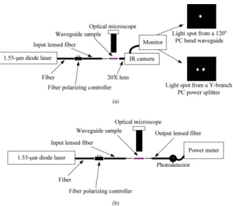
Fig. 11. Schematic of the optical measurement setup. (a) Light spot observa-tion. (b) Output power measurement.
VII. OPTICALMEASUREMENTSYSTEMSETUP
The light of a 1.55- m wavelength launched from a diode laser (Newport LD-1550-21B) was polarized with TE-like or TM-like mode by a fiber polarizing controller (Newport F-POL-PC). Then, the light was coupled into an input ridged ARROW-B structure by a lensed fiber. Next, the light from an output ridged ARROW-B structure was first collected with a lens and an infrared (IR) camera (Electrophysics 7290) to observe the light transmission ability, as shown in Fig. 11(a). The observed images indicated that fabricated ARROW-B PCWs had light bend ability and power-split ability. Then, the IR camera was removed and the output signal from an output ridged ARROW-B structure was received by a lensed fiber with a photodetector (Newport 918D-IG-OD3) and a power meter (Newport 2935-C) to read the output power value, as shown in Fig. 11(b).
VIII. CHARACTERIZATION OFARROW-B 60 AND120 PC
BENDWAVEGUIDES
For evaluating the average bend loss, on a chip we designed five bend PCW samples with the same lateral shift distance of 12.8 m and five bend PCW samples with the same lateral shift distance of 25.6 m. The average 60 and 120 PC bend losses for a chip were evaluated by the average output powers of five same bend PCWs normalized to five same straight PCWs. The evaluating results for 60 and 120 PC bend waveguides are shown in Tables I and II, respectively.
From Tables I and II, it is found that both TE-like and TM-like modes have sharp-bend ability. For the SiN layer as the PCW core layer with the triangular lattice, there is no TM bandgap, so the TM mode cannot be well confined in the straight PCW. However, from previous investigations, a geometry-optimized bend corner could provide a broad-band transient index-guiding bend support for both polarization [10]. From our experimental results of PC bend efficiencies, it is also shown that the TE-like mode could be well confined with both index-guiding support and photonic bandgap-guiding effect in the lateral direction; the
TABLE I
AVERAGEBENDLOSSES OF THETE-LIKE ANDTM-LIKEMODES INDESIGNED
60 PC BENDWAVEGUIDES FORFIVECHIPS: (A) 12.8- MSHIFTDISTANCE AND(B) 25.6- MSHIFTDISTANCE
TABLE II
AVERAGEBENDLOSSES OF THETE-LIKE ANDTM-LIKEMODES INDESIGNED
120 PC BENDWAVEGUIDES FORFIVECHIPS: (A) 12.8- MSHIFTDISTANCE AND(B) 25.6- MSHIFTDISTANCE
TM-like mode could be still well confined with index-guiding support in the lateral direction. In the vertical direction, the light for both polarizations could be well confined with the an-tiresonant reflection. It shows that our fabricated ARROW-B PCW for both polarizations could provide a good transmission through a capsule-shaped sharp-bend corner.
IX. CHARACTERIZATION OFARROW-B Y-BRANCHPC
POWERSPLITTERS
On a chip two kinds of separation distances (25.6 and 51.2 m) of Y-branch PC power splitters were designed to verify the power split ability. To evaluate the average power imbalances on a chip, each kind of the power splitter consisted of five same samples, respectively. Table III shows the average power im-balances of the five chips for TE-like and TM-like modes. The power imbalances were all lower than 0.7 dB for both polariza-tions. It shows that our fabricated Y-branch PC power splitters could provide a good power-split ability for both polarizations.
X. CONCLUSION
Si-based ARROW-B PCWs with 60 bend, 120 bend, and Y-branch power splitter were first successfully designed, fab-ricated, and characterized. This waveguide structure has a rel-atively large core size suitable for the coupling with a single-mode fiber. A simple capsule-shaped design instead of time-consuming topography optimization was applied for the bend
corner and Y-junction region to increase the light bend ability and power-split ability, respectively. It has an easy fabrication advantage in the etching process because of a large defect size. From preliminary experiments, the average bend losses of 60 and 120 PC bend waveguides for both polarizations were lower than 1.5 and 4.2 dB/bend, respectively. Although there was no TM bandgap in our designed ARROW-B PCWs, both TE-like and TM-like modes through the capsule-shaped 60 and 120 PC bend corners could still be well confined with both index-guiding and photonic bandgap-index-guiding confinement in the lat-eral direction and antiresonant reflection in the vertical direc-tion. For the Y-branch PC power splitters, the power imbal-ances for both polarizations were all lower than 0.7 dB. It shows that our fabricated ARROW-B PCWs can provide good light sharp-bend ability and power-split ability for both polarizations. It has a potential to be further applied for the development of PICs in C-band and L-band optical communications.
REFERENCES
[1] E. Yablonovitch, “Inhibited spontaneous emission in solid-state physics and electronics,” Phys. Rev. Lett., vol. 58, no. 20, pp. 2059–2062, 1987.
[2] S. John, “Strong localization of photons in certain disordered dielectric superlattices,” Phys. Rev. Lett., vol. 58, no. 23, pp. 2486–2489, 1987. [3] A. Chutinan, M. Okano, and S. Noda, “Wider bandwidth with high
transmission through waveguide bends in two-dimensional photonic crystal slabs,” Appl. Phys. Lett., vol. 80, no. 10, pp. 1698–1700, 2002. [4] A. Mekis, J. C. Chen, I. Kurland, S. Fan, P. R. Villeneuve, and J. D. Joannopoulos, “High transmission through sharp bends in photonic crystal waveguides,” Phys. Rev. Lett., vol. 77, no. 18, pp. 3787–3790, 1996.
[5] P. I. Borel, L. H. Frandsen, M. Thorhauge, A. Harpøth, Y. X. Zhuang, M. Kristensen, and H. M. H. Chong, “Efficient propagation of TM po-larized light in photonic crystal components exhibiting band gaps for TE polarized light,” Opt. Exp., vol. 11, no. 15, pp. 1757–1762, 2003. [6] M. Augustin, H. J. Fuchs, D. Schelle, E. B. Kley, S. Nolte, and A.
Tun-nermann, “Highly efficient waveguide bends in photonic crystal with a low in-plane index contrast,” Opt. Exp., vol. 11, no. 24, pp. 3284–3289, 2003.
[7] L. H. Frandsen, P. I. Borel, Y. X. Zhuang, A. Harpøth, M. Thorhauge, and M. Kristensen, “Ultralow-loss 3-dB photonic crystal waveguide splitter,” Opt. Lett., vol. 29, no. 14, pp. 1623–1625, 2003.
[8] C. Z. Zhou, Y. Z. Liu, and Z. Y. Li, “Waveguide bend of 90 in two-di-mensional triangular lattice silicon photonic crystal slabs,” Chin. Phys.
Lett., vol. 27, no. 8, p. 084203, 2010.
1707–1713, Jun. 2010.
[14] K. Inoue, Y. Sugimoto, N. Ikeda, Y. Tanaka, K. Asakawa, H. Sasaki, and K. Ishida, “Ultra-small photonic-crystal-waveguide-based Y-split-ters useful in the near-infrared wavelength region,” Jpn. J. Appl. Phys., vol. 43, no. 4A, pp. 446–448, 2004.
[15] Y. Zhang and B. J. Li, “Ultracompact waveguide bends with simple topology in two-dimensional photonic crystal slabs for optical commu-nication wavelengths,” Opt. Lett., vol. 32, no. 7, pp. 787–789, 2007. [16] S. H. Tao, M. B. Yu, J. F. Song, Q. Fang, R. Yang, G. Q. Lo, and D.
L. Kwong, “Design and fabrication of a line-defect bend sandwiched with air trenches in a photonic crystal platform,” Appl. Phys. Lett., vol. 92, no. 3, p. 031113, 2008.
[17] B. L. Miao, C. H. Chen, S. Y. Shi, J. Murakowski, and D. W. Prather, “High-efficiency broad-band transmission through a double-60 bend in a planar photonic crystal single-line defect waveguide,” IEEE Photon.
Technol. Lett., vol. 16, no. 11, pp. 2469–2471, Nov. 2004.
[18] Y. L. Yang, S. H. Hsu, M. F. Lu, and Y. T. Huang, “Photonic crystal slab waveguides based on antiresonant reflecting optical waveguide structures,” J. Lightwave Technol., vol. 27, no. 14, pp. 2642–2648, Jul. 2009.
[19] Y. L. Yang, “Investigation on ARROW-based photonic crystal wave-guide devices and 3D copper photonic crystals,” Ph.D. dissertation, Na-tional Chiao-Tung University, Hsinchu, Taiwan, 2009.
[20] A. V. Lavrinenko, A. Novitsky, and V. V. Zhilko, “ARROW-based silicon-on-insulator photonic crystal waveguides with reduced losses,”
Opt. Quant. Electron., vol. 38, pp. 815–826, 2006.
[21] T. Baba and Y. Kokubun, “New polarization-insensitive antiresonant reflecting optical waveguide (ARROW-B),” IEEE Photon. Technol.
Lett., vol. 1, no. 8, pp. 232–234, Aug. 1989.
[22] J. P. Hulme and S. S. A. An, “The application of leaky anti-resonant reflecting optical waveguides as optical sensors (L-ARROW),” Sens.
Actuators B, vol. 138, pp. 42–47, 2009.
[23] C. C. Huang, “Real-time detection of -thrombin binding to single-strand DNA aptamers and dengue virus DNA hybridization by ARROW-B SPR biosensors,” Master thesis, National Chiao-Tung University, Hsinchu, Taiwan, 2008.
[24] S. Ikuta, T. Sekimoto, W. Pan, S. T. Chu, and Y. Kokubun, “High-cou-pling efficiency vertical ARROW coupler with large tolerance and short coupling length for three-dimensional optical interconnects,”
IEEE Photon. Technol. Lett., vol. 11, no. 8, pp. 1006–1008, Aug. 1999.
[25] T. Baba and Y. Kokubun, “Dispersion and radiation loss characteristics of antiresonant reflecting optical waveguides—Numerical results and analytical expressions,” IEEE J. Quantum Electron., vol. 28, no. 7, pp. 1689–1700, Jul. 1992.
[26] T. Tamir, Guided-Wave Optoelectronics. New York: Springer-Verlag, 1990.
[27] A. Mekis, S. Fan, and J. D. Joannopoulos, “Bound states in photonic crystal waveguides and waveguide bends,” Phys. Rev. B, vol. 58, no. 8, pp. 4809–4817, 1998.
![TraditionalMLCalgorithmsmainlytacklethebatchMLCproblem,wheretheinputdataarepresentedinabatch[24,28].Nevertheless,inmanyMLCapplicationssuchase-mailcategorization[22],multi-labelexamplesarriveasastream.Onlineanalysisistherefore dimensionreducermotivatedbyma](data:image/gif;base64,R0lGODlhAQABAIAAAP///wAAACH5BAEAAAAALAAAAAABAAEAAAICRAEAOw==)