All-optical switching with pulsed signals in an
all-semiconductor-optical-ampli®er loop device
J.-H. Lee
a, C.C. Yang
a,*, M.C. Shih
b, T.J. Chuang
c,daDepartment of Electrical Engineering and Graduate Institute of Optical Engineering, National Taiwan University, 1, Roosevelt Road,
Sec. 4, Taipei, Taiwan, ROC
bInstitute of Optical Sciences, National Taiwan Ocean University, Keelung, Taiwan, ROC cCenter for Condensed Matter Sciences, National Taiwan University, Taipei, Taiwan, ROC
dInstitute of Atomic and Molecular Sciences, Academia Sinica, Taipei, Taiwan, ROC
Received 20 June 2000; accepted 15 September 2000
Abstract
Picosecond pulsed-signal operation for ecient self- and cross-switching in an all-semiconductor-optical-ampli®er loop device was implemented. Although the con®guration of the device is similar to a conventional nonlinear optical loop mirror, the operation principles are quite dierent. For cw signals, the device operation relies on the nonlinear coupling eect in a multi-mode interference waveguide ampli®er and the lateral ®eld redistribution and ampli®cation by the active loop. However, for pulsed signals the crucial factor of asymmetric gain distribution in the loop needs to be added for the device operation. The pump±probe experiments provided ecient cross-switching results and indicated that GHz-range operation is feasible by redesigning the device con®guration for pump signal injection. Ó 2000 Elsevier Science B.V. All rights reserved.
Nonlinear optical loop mirrors (NOLMs) and their derivatives are important optoelectronics devices for all-optical switching with the applica-tions to high-speed signal processing and optical communications [1±5]. Typically, such a device consists of either an all-®ber loop or a ®ber loop asymmetrically inserted with a semiconductor op-tical ampli®er (SOA). The ®ber loop is connected with a ®ber coupler for input/output coupling. The required optical nonlinearity for all-optical switching comes from either the Kerr eect in ®ber
or gain saturation in the SOA. The ®ber loop length of such a device ranges from a few tenths to a few meters, which corresponds to a latency of >1 ns. Recently, all-semiconductor devices with the NOLM con®guration have received attention for their advantages of low latency, easy integra-tion, compactness, mass producintegra-tion, and low cost [6±8].
In this letter, we report the experimental results of all-optical switching in an all-SOA loop device with pulsed signals. These results represent a sig-ni®cant progress of ours in realizing a practically useful device. The experimental results and theo-retical modeling with cw-signal operation of such a device have been reported in Refs. [7,8]. In such a device, a multi-mode interference waveguide Optics Communications 185 (2000) 393±397
www.elsevier.com/locate/optcom
*Corresponding author. Tel.: 2-2365-7624; fax:
+886-2-2365-2637.
E-mail address: [email protected] (C.C. Yang).
0030-4018/00/$ - see front matter Ó 2000 Elsevier Science B.V. All rights reserved. PII: S0030-4018(00)01016-6
ampli®er (MMIWA) was connected to the SOA loop for input/output coupling. In the cw opera-tion, it was found that the observed nonlinear switching came from the combined eect of the nonlinear coupling in the MMIWA, and the lateral wave ®eld redistribution plus ampli®cation caused by the loop. In this situation, the loop asymmetry did not contribute to the observed nonlinear switching phenomena. However, in the pulsed-signal operation the loop asymmetry becomes crucially important.
Fig. 1 shows the layout of the device. The active loop of 300 lm in radius is formed with a curved ridge waveguide with a ridge width of 4 lm (a single-mode waveguide). The loop is connected to an MMIWA with a length of 460 lm and a ridge width of 8 lm. The MMIWA serves the function of the coupler with the nonlinear coupling eect. Then, the input and output legs are formed with 4 lm wide SOAs. Both have the lengths of about 600 lm. The device was fabricated on a four-period GaAs/AlGaAs multiple quantum well epit-axial structure. The GaAs wells (10 nm thick) and Al0:25Ga0:75As barriers (20 nm) were sandwiched
by two 140 nm thick i-Al0:25Ga0:75As separate
con®nement layers, and p-Al0:6Ga0:4As and
n-Al0:6Ga0:4As cladding layers.
Electro-lumines-cence measurements indicated that the gain peaks
in the transverse electric (TE) and transverse magnetic (TM) directions were 834 and 817 nm, respectively. The fabrication procedures were the same as the typical processes for semiconductor lasers except the etching technique for forming the ridge waveguides. To achieve vertical and smooth etched walls for reducing bending loss and to minimize surface damage, the UV laser-assisted cryo-etching technique was used [9]. The etching depth was 1.6 lm. For injecting dierent currents into dierent areas, we divided the electro-pad into four disconnected regions, indicated by the
injection currents I1 (input±output region), I2
(MMIWA), I3 (one-quarter of the loop), and I4
(three-quarter of the loop).
In experiments, 100-fs pulses from a mode-locked Ti:sapphire laser were ®rst passed through a monochromator for selecting the required center wavelengths and spectral widths of input signals. With a ®xed center wavelength of the fs pulse from the laser, the allowed wavelength range for selec-tion was about 10 nm. After the monochromator, the pulse of a selected wavelength had a width of about 1.4 ps. Such signals were end coupled into the input leg of the device. The signals emergent from the output leg were passed through another monochromator for ®ltering out ampli®ed spon-taneous emission noise. Other details of the ex-perimental procedures can be found in Ref. [8]. Fig. 2 provides three sets of data showing power-dependent switching when the TE-polarized input signals at 834 nm (TE gain peak) were used. Note that in Figs. 2±5, the continuous curves are drawn to best ®t the data points for guiding the eyes. The horizontal axis represents the average input power before entering the input leg. The injection current values of I1, I3, and I4 were ®xed at 40, 200, and
100 mA, respectively. Note that this arrangement leads to the injection current density ratio of the one-quarter section over the three-quarter section of the loop to be about 6:1. The three curves in Fig. 2 correspond to the I2 values (into
the MMIWA region) at 25, 50, and 75 mA, re-spectively. One can see that signi®cant nonlinear
switching occurs when I2 is suciently large.
Generally speaking, a larger I2 leads to a smaller
switching power. It is noted that the input power level in Fig. 2 is two orders of magnitude smaller Fig. 1. Schematic diagram of the
all-semiconductor-optical-ampli®er loop device. The electrode pad is divided into four disconnected sections denoted by I1through I4.
Fig. 2. Output power level as a function of input power with dierent I2values. The input signal is TE polarized at 834 nm.
I1 40 mA, I3 200 mA, and I4 100 mA.
Fig. 3. Output power level as a function of input power with dierent I3values. The input signal is TE polarized at 834 nm.
I1 40 mA, I2 50 mA, and I4 100 mA.
Fig. 4. Output power level as a function of input power with dierent signal wavelengths. The input signal is TE polarized. I1 40 mA, I2 50 mA, I3 200 mA, and I4 100 mA.
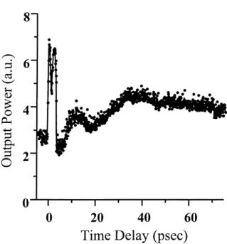
Fig. 5. Probe signal power level as a function of the time delay from a pump±probe experiment. The pump is TM polarized at 825 nm and has a power of 0.75 mW. The probe is TE polarized at 834 nm and has a power of 0.25 mW. I1 40 mA, I2 50
than its counterpart in Ref. [8] (see Fig. 4 of this paper), con®rming that the pulsed-signal opera-tion is much more ecient for all-optical switch-ing. For instance, 0.6 mW switching power in the horizontal axis of Fig. 2 corresponds to a switch-ing energy of 79 fJ if 1% of input couplswitch-ing e-ciency is assumed.
Fig. 3 demonstrates three sets of data with I3
varied from 180 to 220 mA. In this ®gure, I1, I2
and I4 were ®xed at 40, 50 and 100 mA,
respec-tively. The signal was still TE polarized with the
center wavelength at 834 nm. The increase of I3
implies the increase of the loop asymmetry and hence the nonlinear switching eciency, as veri®ed by the results in Fig. 3. Then, Fig. 4 demonstrates the nonlinear switching results at dierent signal wavelengths. With I1, I2, I3, and I4 ®xed at 40, 50,
200, and 100 mA, respectively, the results of three wavelengths of the TE-polarized signal at 830, 834, and 838 nm are shown. Here, one can see that wavelength choice is quite critical for ecient nonlinear switching. Ecient switching can be observed only near the gain peak.
To observe the cross-switching eect, we pre-pared two ps pulses for pump±probe experiments. Fig. 5 shows a typical result of the pump±probe experiments for the probe output power level as a function of the pump±probe time delay. Here, the pump was TM polarized at 825 nm with the input power at 0.75 mW and the probe was TE polarized at 834 nm with the input power at 0.25 mW. The injection current values were the same as those in Fig. 4. The zero time delay was approximately set at the ®rst peak of the data curve. One can see the narrow two-hump feature of about 5 ps in width around the zero time delay. It is supposed to cor-respond to the situation that the pump and probe overlap in most part of the device. After the two-hump feature, a long tail in an oscillatory manner can be observed. This long tail is supposed to come from the period of gain recovering from saturation in the MMIWA and loop. Its length should be in the order of carrier lifetime (several hundred ps to a few ns). The oscillatory manner in either the two-hump peak or the tail can be attributed to the interferometry nature of the loop device. From several sets of pump±probe data, we can induce that the period of the oscillation increases with
time delay. Also, a valley always exists between the peak feature and the long tail. The interpretations for these phenomena require a sophisticated model of the device.
In interpreting the device operation with cw signals, we considered the nonlinear coupling ef-fect in the MMIWA and the functions of the lat-eral ®eld redistribution and ampli®cation from the loop [8]. Such considerations are still valid. However, with pulsed signals the loop asymmetry needs to be considered. The nonlinear coupling in the MMIWA results in power-dependent lat-eral ®eld distribution. After splitting into the two counter-propagating components in the loop, they experience dierent gain levels and phase shifts in the asymmetric loop. Such dierences combine with the nonlinear coupling eect acquired during the backward propagation in the MMIWA to give various distributions of the signal power between the input and output legs. When the pump±probe experiment is conducted, the nonlinear coupling process of the strong pump signal dominates the lateral ®eld distribution of the probe signal in the MMIWA. Also, the asymmetric gain satura-tion due to the counter-propagating pump sig-nals may enhance the asymmetric gain and phase factors for the counter-propagating probe signals. Such complicated processes result in the observed cross-switching phenomenon, shown in Fig. 5.
In summary, we have demonstrated the pulsed-signal operation in an all-SOA loop device. E-cient all-optical switching was implemented. The pulsed-signal operation of the device was quite dierent from that of cw signals. Besides the lat-eral ®eld redistribution and ampli®cation by the loop, and the nonlinear coupling eect in the MMIWA, the asymmetry in gain distribution along the loop was crucially important for the pulsed operation. Experimental results have shown quite ecient self- and cross-switching. Further investigations include the modeling of the pulsed operation of such a device and the design of device con®guration for reducing the decay time of non-linear switching [4]. Meanwhile, the fabrication of such a device operated near 1550 nm would make their applications for ®ber communications prac-tical.
Acknowledgements
This research was supported by National Sci-ence Council, The Republic of China, under the grants of NSC 88-2112-M-002-004, NSC 88-2215-E-002-012, and NSC 88-2215-E-002-014.
References
[1] J. Cai, K. Feng, X.P. Chen, A.E. Willner, Equalization of nonuniform EDFA gain using a ®ber-loop mirror, IEEE Photon. Technol. Lett. 9 (1997) 916±918.
[2] W.S. Wong, S. Namiki, M. Margalit, H.A. Haus, P. Ippen, Self-switching of optical pulses in dispersion-imbal-anced nonlinear loop mirrors, Opt. Lett. 22 (1997) 1150± 1152.
[3] D. Wang, E.A. Golovchenko, A.N. Pilipetskii, C.R. Menyuk, M.F. Arend, Nonlinear optical loop mirror based on standard communication ®ber, J. Lightwave Technol. 15 (1997) 642±646.
[4] J.P. Sokolo, P.R. Prucnal, I. Glesk, M. Kane, A terahertz optical asymmetric demultiplexer (TOAD), IEEE Photon. Technol. Lett. 5 (1993) 787±790.
[5] M. Eiselt, W. Pieper, H.G. Weber, SLALOM: semiconduc-tor laser ampli®er in a loop mirror, J. Lightwave Technol. 13 (1995) 2099±2112.
[6] E. Jahn, N. Agrawal, W. Pieper, H.J. Ehrke, D. Franke, W. Furst, C.M. Weinert, Monolithically integrated non-linear Sagnac interferometer and its application as a 20 Gbit/s all-optical demultiplexer, Electron. Lett. 32 (1996) 782±784.
[7] J.H. Lee, D.A. Wang, H.J. Chiang, D.W. Huang, S. Gurtler, C.C. Yang, Y.W. Kiang, B.B. Chen, M.C. Shih, T.J. Chuang, Nonlinear switching in an all-semiconductor-optical-ampli®er loop device, IEEE Photon. Technol. Lett. 11 (1999) 236±238.
[8] J.H. Lee, D.A. Wang, Y.W. Kiang, H.J. Chiang, C.C. Yang, Nonlinear switching behaviors in a compact all-semiconductor-optical-ampli®er Sagnac interferometer de-vice, IEEE J. Quant. Electron. 35 (1999) 1469±1477. [9] C.-H. Tsai, J.-H. Lee, H.-J. Chiang, C.C. Yang, M.C. Shih,
B.C. Chen, T.J. Chuang, Y. Chang, Semiconductor circu-lar ring lasers fabricated with the cryo-etching technique, IEEE Photon. Technol. Lett. 10 (1998) 751±753.