Digital VLSI OFDM Transceiver Architecture for
Wireless SoC Design
Wei-Hsiang Tseng, Ching-Chi Chang, and Chorng-Kuang Wang
Graduate Institute of Electronic Engineering and Department of Electrical EngineeringNational Taiwan University Taipei 106, Taiwan R.O.C. ckwang@cc.ee.ntu.edu.tw
Abstract—This paper presents the VLSI architecture of an
OFDM baseband transceiver for wireless communications. The open-/closed-loop carrier recovery achieves the stepping frequency acquisition for high-band RF systems, and the proposed timing recovery cooperated with the self-correcting interpolation realizes an OFDM baseband digital IP design. Hardware sharing and power-of-2 coefficients fulfill this compact transceiver system chip. Simulations show that the receiver can deliver 10% packet error rate (PER) requirement under all specified SNRs for IEEE 802.11a. Using the typical 0.25µm CMOS technology, the chip occupies 3.5×3.5 mm2 area
and consumes 109 mW under 2.5 V power supply.
I. INTRODUCTION
The demand of wide-band communications leads to a tremendous growth of wireless LAN. In 1997, the IEEE 802.11 standard was first established for the wireless LAN. It supports the data rates of 1 and 2Mbps which are not sufficient for many multimedia applications. The IEEE 802.11a standard was proposed for efficient bandwidth utilization, which selects orthogonal frequency division multiplexing (OFDM) as the basis for the physical layer and supports the data rates from 6 up to 54 Mbps in the 5 GHz band. OFDM has been recognized as an optimal solution to combat burst noises and the multi-path fading.
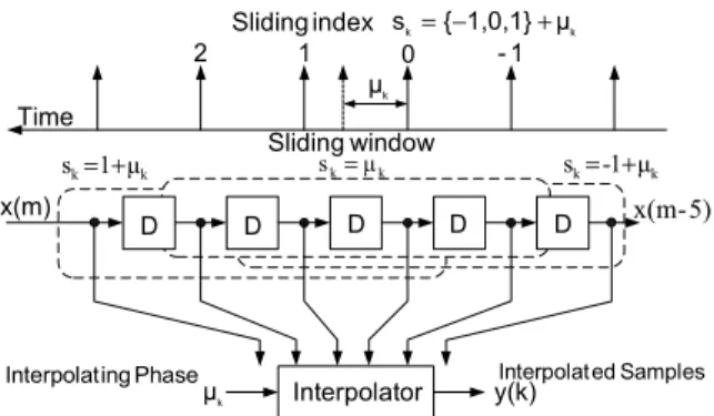
Since the transmission data format is clearly specified in communication systems [1], how to utilize the limited signaling resources to design a practical and robust receiver becomes a tough challenge. Whereas the significant drawback of OFDM systems is the sensitivity to synchronization errors, the multi-step recovery and precise adaptation techniques represent nowaday wide-band VLSI system design methodologies. In order to realize a digital transceiver IP, the digitally self-compensating solution of the timing recovery is preferable [8]. Using an interpolator with a long buffer can solve the problem of sample stuffed or rubbed when the timing frequency offset (TFO) occurs [8]. However, the buffer size may be infinite in non-stopping transmissions and it is impractical. We propose the interpolator architecture with a sliding window to realize the self-adjustment of sample skipping or duplicating, which prevents the conventional digital timing recovery from fatal jitter problem caused by illegal indexing.
Mapping QAM Insertion Pilot Stream Bit Input ToDAC or Interpolat ↓2 Derotator Filter Match Correlator Delay Prefix Cyclic Remove Windowing FFT FEQ Estimation Channel Block Decision Extraction Tone Pilot Detector Error Timing Detector Error Carrier Estimation Frequency Carrier Correction Frequency Carrier Filter Loop Detection Boundary Symbol Filter Loop Control or Interpolat IFFT Prefix Cyclic Add Generator Sequence Training 2 ↑ WaveShaping Stream Bit Output r Transmitte Receiver ADC From x(m) y(k)
Fig. 1. The proposed transceiver architecture.
This paper organizes as follows. Section II presents the proposed baseband transceiver architecture. Section III shows the circuits of the functional blocks in the receiver. The simulation environment and the evaluation of the designed system are delivered in Section IV. Section V shows the chip layout and the post-layout summary. Finally, the conclusions are given in Section VI.
II. TRANSCEIVER ARCHITECTURE
The proposed baseband transceiver architecture is shown in Fig. 1 where the upper part is the transmitter and the lower one is the receiver. The transmitter mainly consists of training sequence generation, QAM mapping, pilot insertion, IFFT, cyclic prefix (CP) extension, windowing, and wave shaping functional blocks. The wave shaping filter adopts a raised cosine filter with a roll-off factor 0.22. The transmitted signal completely complies with the power spectrum mask requirement [1].
In the receiver, other than an interpolator, a symbol boundary detector, a de-rotator, a delay correlator, a match filter, and a FFT unit, the receiving chain also includes a multi-step carrier recovery loop, a self-correcting timing recovery loop, and an adaptation aided frequency-domain equalizer (FEQ). FFT and IFFT functions share the resource in a single architecture.
Wei-Hsiang Tseng is currently with MediaTek Inc., Taiwan, R.O.C.. This program is supported by the National Science Council (NSC), Taiwan, R.O.C..
5794
0-7803-8834-8/05/$20.00 ©2005 IEEE.
on Acquisiti AGC Detection Signal Estimation BoundaryCoarseSymbol Tracking CFO Estimation Boundary Symbol Fine Estimation CFO Coarse
EstimationFineCFO
Estimation Channel Tracking TFO FEQ Adaptive Time Preamble Long Preamble
Short LENGTH RATE SERVICE+DATA DATA
1
T T2
GI GISIGNAL GI Data1 GI Data2
1 t t2t3t4t5t6t7t8t9t10 s 8 3.2x2 1.6+ =µ s 8 0.8x10=µ s 16 8 8+= µ s 4 3.2 0.8+ =µ s 4 3.2 0.8+ =µ
Fig. 2. The training process of the receiver design.
III. RECEIVER DESIGN A. Training Process
The training process designed in the receiver is shown in Fig. 2. The first part of the short preamble, about 4.8 µs, is reserved for signal arriving detection and AGC acquisition. The remaining short preamble is utilized for the coarse symbol boundary detection and the carrier frequency offset (CFO) compensation. Then, the fine symbol boundary detection, the fine CFO estimation, and the channel estimation are finished in the duration of the long preamble. The residual CFO, the TFO, and the coefficients of the FEQ are adaptive tracked after the preamble.
B. Coarse and Fine Symbol Boundary Detections
The receiver has to extract the FFT interval within the consecutive received samples. In the short preamble period, the delay correlator moves over the ten repetitive intervals to detect the coarse symbol boundary. A mechanism basing on the binary search algorithm is proposed to track the maximum value of the correlation. Following the short preamble, the long-preamble matched filter is exploited to squeeze the exact symbol boundary. When the symbol boundary detection is finished, the receiver removes the CP and the FFT demodulates the remaining samples. C. Multi-step Carrier Recovery
The OFDM system is sensitive to the CFO. Both amplitude reduction caused by phase shift and the inter-carrier inference (ICI) severely worsen the packet error rate (PER) [2]. The proposed carrier recovery has three steps. Based on the maximum likelihood estimation [3], the 16-tap delay correlator devised in the symbol boundary detector also achieves the coarse CFO estimation in the short preamble period. Then, a 64-tap delay correlator further completes the fine CFO compensation in the long preamble. Table I lists the performance summaries of the open-loop CFO estimations. By means of the pilots imbedded in the OFDM symbols, the remaining CFO is adaptive tracked by a phase-locked loop (PLL) [4]. The estimated carrier frequency error, εc,f, is
(1) , ) ( 1 2 1 ) ( , 1, , = ⋅
∑
∠ −∠ − i i n i n i Symbol f c Y Y N T n π εwhere i∈[-21, -7, 7, 21] [5]. Yn,i is the equalized constellation point
in the ith sub-carrier of the nth OFDM symbol. TSymbol is the symbol
duration and Ni denotes the number of the pilots which is 4 in this
design. Correspondingly, the estimated carrier phase error, εc,phase, is
TABLE I. SUMMARY OF THE CFOESTIMATION
CFO Estimation Type Coarse Fine
Estimation Range ± 625 KHz ± 156 KHz
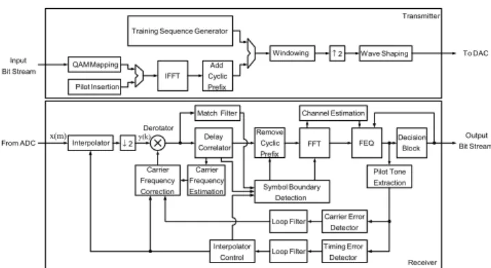
Maximum Estimation Error ± 32.6 KHz ± 6.22 KHz
TABLE II. DESIGN PARAMETERS OF THE CARRIER RECOVERY LOOP
Parameter Value
Lock-in Range ∆ωL 7.5 KHz
Damping Factor ξ 0.707
Natural Frequency ωn 3.3 x 10⁴ rad/s
Phase Detector Gain Kd 1 unit/rad
NCO Gain Ko 20 MHz/unit
PI Filter Coefficient C1 2-11 PI Filter Coefficient C2 2-14 Output Input 2 C 1 C -1 Z Fig. 3. PI filter (2) . 1 ) ( 2 ) ( , 0 , , =
∑
⋅ =∑
∠ = i i n i n k Symbol f c phase c Y N T n n πε εThe proportional-and-integral (PI) filter shown in Fig. 3 stands the loop filter in the PLL. Table II lists the design parameters of the adaptive carrier recovery loop. To eliminate multiplications, the coefficients of the PI filter are truncated to power-of-2 numbers. In our design, the performance degradation caused by residual CFO can be suppressed down to 0.1 dB.
D. Self-correcting Timing Recovery
The design of the timing recovery adopts an all-digital solution with a Farrow interpolator [6] mounted after the free running analog-to-digital (A/D) converter. The conventional all-digital timing recovery designs ignored that the drifting interpolation phase due to the TFO would jump beyond sample boundaries to induce either sample stuffing or rubbing [7]. The large sampling jitters could crash the signal detection. Therefore, skipping or duplicating samples in the CP is required to reset the interpolating phase [8]. In order to combine the Farrow interpolator with the skip/duplicate process in the view of VLSI, we propose the architecture of the interpolator with a sliding window as shown in Fig. 4 which adds two additional delay registers for the original Farrow structure. The self-correcting timing recovery automatically slides the window,
sk=1+µk or sk=-1+µk, to fit the boundary-crossed interpolating
phases in the reception of the samples within the FFT period and skips/duplicates a sample of the CP at the start of the next received
OFDM symbol to reset the windowing position, sk=µk. The
hardware implementation is given in Fig. 5. A PLL is also used to adaptively track the TFO, and the PI filter is chosen as the loop filter in the timing recovery loop. The estimated sampling frequency error, εs,f, is
D or Interpolat k µ Time k k { 1,0,1} µ s = − + index Sliding 0 1 -1 2 window Sliding y(k) x(m) D D D D Phase ing
Interpolat InterpolatedSamples
k µ k k -1 µ s = + k k 1 µ s = + sk=µk 5) -x(m
Fig. 4. The proposed interpolator with the sliding window.
1/2 − r Multiplexe : x(m) k µ y(k) D D D D D D D D D
Fig. 5. Implementation of the interpolator with the sliding window.
[
( ) ( )]
, (3) 1 1 2 1 ) ( . , 1 , 1 , , , = ⋅∑
− ∠ −∠ − ∠ − −∠ − j i j n i n j n i n ij sample f s n T N i j Y Y Y Y π εwhere i, j∈[-21, -7, 7, 21] [5] and Tsample is the sample period. The
sampling phase error, εs,phase, is
[
( ˆ ˆ )]
, (4) 1 ) ( 2 ) ( . , , 0 , ,∑
∑
∠ −∠ − = ⋅ = = ij j n i n ij s n k Symbol f s phase s Y Y j i N N T n n πε εwhere Ns denotes the number of the samples in an OFDM symbol.
Table III lists the parameters of the timing recovery loop. E. FFT/IFFT
The 64-point pipeline FFT/IFFT processor is implemented with the radix-2/4/8 algorithm [9] in the single-path delay feedback (SDF) architecture. For a 64-point FFT/IFFT, it can be divided into two pipeline stages, and only one complex multiplier is required. The SQNR of the FFT/IFFT is 46.8 dB for this transceiver design. F. Frequency-domain Equalizer
The FEQ exploits the minimum mean square error (MMSE) criterion [10] to perform the channel estimation in the end of the long preamble,
TABLE III. DESIGN PARAMETERS OF THE TIMING RECOVERY LOOP
Parameter Value
Lock-in Range ∆ωL 1.9 KHz
Damping Factor ξ 0.707
Natural Frequency ωn 8.5 x 10³ rad/s
Phase Detector Gain Kd 0.18 unit/rad
NCO Gain Ko 40 MHz/unit
PI Filter Coefficient C1 2-12 PI Filter Coefficient C2 2-17 C f ∆ S S f f +∆ ) (t h LPF CFO Offset Frequency Sampling Channel Multipath r Transmitte AWGN Model Channel Equivalent Baseband Receiver
Fig. 6. The simulation environments.
5 10 15 20 25 30 35 0 0.1 0.2 0.3 0.4 0.5 0.6 0.7 0.8 0.9 1 SNR (dB)
Packet Error Rate (PER)
BPSK QPSK 16QAM 64QAM
Fig. 7. PER performance for the channel delay spread 0 ns.
, } / /{ 2 2 2 s n K K K H H C = ∗ +σ σ (5)
where CK and HK are the equalization coefficient and the channel
frequency response at the Kth sub-carrier, respectively. And σn2 is
the variance of the AWGN while σs2 is the variance of the
transmitted symbols. The least mean square (LMS) algorithm is adopted to adaptively update the coefficients [11],
, ) ( ) 1 (+ = +∆ ∗ K K j K j K C Y C ε (6) where CK(j) is the jth coefficient at the Kth sub-carrier, YK is the FFT
demodulated output, εK is the decision error, and ∆ is the scale
factor. The additional LMS algorithm improves the equalization performance about 3 dB SNR.
IV. SIMULATION RESULTS
Multipath fading, CFO, TFO, and AWGN are taken into account in the simulation environments as shown in Fig. 6. The indoor multipath channel model is Saleh’s one [12]. In the IEEE 802.11a standard, a PER less than 10% is required for 1000 bytes transmissions [1]. Fig. 7, 8, and 9 show the simulation results of the PER performances, which contain the cases of the delay spread equal to 0 ns, 50 ns, and 100 ns with the maximal tolerable CFO and TFO. The maximal tolerable CFO is ± 40 ppm of the local oscillator (LO) frequency, 5.8 GHz, in the zero-IF architecture and the maximal tolerable TFO is ± 40 ppm of the A/D sampling rate, 40 MHz, in this design.
V. CHIP LAYOUT AND PERFORMANCE SUMMARY
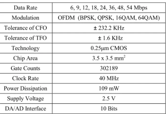
Fig. 10 shows the chip layout. Total gate counts are about 302K. The bit numbers of both interfaces of the A/D and D/A converters are 10 bits. Using cell-based design methodologies, this chip is implemented in 0.25µm CMOS technology and occupies
3.5×3.5 mm2 chip area. With 2.5 V supply voltage, the power
dissipation is 109 mW. The performance summary is listed in Table IV.
VI. CONCLUSIONS
This paper presents the VLSI architecture of an OFDM digital baseband transceiver for wireless LAN systems. The 3-step carrier recovery acquires the coarse carrier frequency with the preliminary two open-loop estimations in the training period and maintains good jitter performances with the pilot aided PLL in the data transmission interval. The self-correcting timing recovery realizes the OFDM transceiver digital IP which can be ideally integrated with the analog-front-end and RF circuits for the SoC design. Because the proposed interpolator with the sliding window adjusts the rational interpolation phases in the cyclic prefix, it can be applied to discrete multi-tone (DMT) and single carrier modulation using frequency domain equalizer (SC-FEQ) systems. The OFDM transceiver realized in the IEEE 802.11a system can provide 10% PER requirement under specified SNRs in the indoor transmission environments. Using 0.25µm CMOS process, this transceiver is implemented in 3.5×3.5 mm2 chip area. The power consumption is 109 mW under 2.5 V power supply.
5 10 15 20 25 30 35 0 0.1 0.2 0.3 0.4 0.5 0.6 0.7 0.8 0.9 1 SNR (dB)
Packet Error Rate (PER)
BPSK QPSK 16QAM 64QAM
Fig. 8: PER performance for the channel delay spread 50 ns.
5 10 15 20 25 30 35 0 0.1 0.2 0.3 0.4 0.5 0.6 0.7 0.8 0.9 1 SNR (dB)
Packet Error Rate (PER)
BPSK QPSK 16QAM 64QAM
Fig. 9. PER performance for the channel delay spread 100 ns.
REFERENCES
[1] Part 11: Wireless LAN medium access control (MAC) and physical layer (PHY) specifications for high-speed physical layer in the 5 GHz band. IEEE std. 802.11a, Nov. 1999.
[2] P. H. Moose, “A technique for orthogonal frequency division multiplexing frequency offset correction,” IEEE Trans. on Comm., Vol. 42, No. 10, pp. 2908-2914, Oct. 1994.
[3] J. J. van de Beek et al., “ML estimation of time and frequency offset in OFDM systems,” IEEE Trans. on Signal Processing, Vol. 45, No. 7, pp. 1800-1805, July 1997.
[4] R.E. Best, Phase-Locked Loops, 3rd ed., McGraw-Hill, 1998. [5] M. Sliskovic, “Carrier and sampling frequency offset estimation and
correction in multicarrier systems,” IEEE GLOBECOM, pp. 285-289, Nov. 2001.
[6] L. Erup et al., “Interpolation in digital modems-part ii: implementation and performance,” IEEE Trans. on Comm., Vol. 41, No. 6, pp. 998-1008, June 1993.
[7] C-F Hsu, Y-H Huang and T-D Chiueh, “Design of an OFDM receiver for high-speed wireless LAN,” ISCAS, Vol. 4, pp. 558-561, May 2001.
[8] T. Pollet and M. Peeters, “Synchronization with DMT modulation,”
IEEE Comm. Mag., Vol. 37, No. 4, pp. 80-86, Apr. 1999.
[9] L. Jia et al., “A new VLSI-oriented FFT algorithm and implementation,” IEEE ASIC Conf., pp. 337-341, Sept. 1998.
[10] H. Sari et al., “Transmission techniques for digital terrestrial TV broadcasting,” IEEE Comm. Mag., Vol. 33, No. 2, pp. 100-109, Feb. 1995.
[11] J. G. Proakis, Digital Communication, 4th ed., McGraw Hill, 2001 [12] A. A. M. Saleh and R. A. Valenzuela, “A statistical model for indoor
multipath propagation,” IEEE J. Selected Areas in Comm., Vol. SAC-5, No. 2, pp. 128-137, Feb. 1987. Filter Shaping Wave Filter Match Correlator Delay or Interpolat IFFT FFT/ Estimation Channel FEQ Estimation CFO Generator Preamble Reversal Bit NCO Derotator Tracking CFO/TFO Control Rx Tx/
Fig. 10. Chip layout
TABLE IV. THE PERFORMANCE SUMMARY OF THIS CHIP
Data Rate 6, 9, 12, 18, 24, 36, 48, 54 Mbps
Modulation OFDM (BPSK, QPSK, 16QAM, 64QAM)
Tolerance of CFO ± 232.2 KHz Tolerance of TFO ± 1.6 KHz Technology 0.25µm CMOS Chip Area 3.5 x 3.5 mm2 Gate Counts 302189 Clock Rate 40 MHz Power Dissipation 109 mW Supply Voltage 2.5 V
DA/AD Interface 10 Bits