使用完全鉬矽化之雙功函數金屬閘極技術
87
0
0
全文
(2) 使用完全鉬矽化之雙功函數金屬閘極技術 Dual Work Function Metal Gate Technology Using Fully Molybdenum Silicidation 研 究 生:何武陵. Student:Ho,Wu-Ling. 指導教授:張俊彥 博士. Advisor:Dr. Chun-Yen Chang 國立交通大學. 電子工程學系. 電子研究所碩士班. 碩 士 論 文. A Thesis Submitted to Department of Electronics Engineering & Institute of Electronics College of Electrical Engineering and Computer Science National Chiao Tung University in partial Fulfillment of the Requirements for the Degree of Master in Electronics Engineering June 2005 Hsinchu, Taiwan, Republic of China. 中華民國九十四年六月. ii.
(3) iii.
(4) 使用完全鉬矽化之雙功函數金屬閘極技術. 研究生:何武陵. 指導教授:張俊彥 博士. 國立交通大學 電子工程學系 電子研究所碩士班. 摘. 要. 我們在金屬氧化物半導體元件閘極結構上提出了一個新的概念 圖,在 N 型元件與 P 型元件的閘極材料分別用鉬的矽化物與純鉬來製 作,這將可以避免掉硼離子的穿隧效應以及獲得良好的熱穩定性。 我們研究使用鉬金屬矽化物薄膜做為金屬氧化物半導體電晶體的閘 極材料及其功函數調變效應,並且探討其平帶電壓與等效介電層厚度對 溫度的熱穩定性。吾人在純氬氣體下,濺渡一層鉬金屬及非晶矽薄膜, 吾人以金屬/二氧化矽/矽基板的電容結構在純氮氣環境下做不同溫度的 快速熱退火處理。並且以同樣製程條件,將鉬金屬與非晶矽濺鍍於由有 機金屬化學氣相沉積法所生長的二氧化鉿介電層薄膜上,並探討其在高 介電值介電層薄膜上形成的鉬金屬矽化物的基本功函數調變效應以及 閘極借電層的熱穩定性。 在功函數調變方面,將鉬金屬矽化物沉積於二氧化矽介電層的閘極 功函數由剛沉積的 4.78 電子伏特經由快速熱退火處理加溫到攝氏 800℃,其功函數可調變至 4.39 電子伏特。而在高介電值二氧化鉿薄膜 上所沉積的鉬金屬矽化物,將使得功函數由 4.81 電子伏特調變至 4.34 iv.
(5) 電子伏特。在這裡並沒有看到費米能階釘鎖現象,這可能是由於費米釘 鎖能階很接近 4.34 電子伏特的原因。接著將砷原子使用離子佈值法加入 至鉬金屬矽化物閘極內,進而使以二氧化矽為介電層的金氧半結構其功 函數調降至 4.001 電子伏特。並且使以二氧化鉿為介電層的元件之功函 數調降至 4.16 電子伏特。 在熱穩定性方面,藉由快速熱退火處理,將鉬金屬與非晶矽的金氧 半結構電容分別加熱從 600℃到 950℃ 30 秒,探討其平帶電壓與等效氧 化層厚度對溫度的變化,發覺無論是以二氧化矽或是高介電常數二氧化 鉿為介電層的金氧半電容在加熱至攝氏 800℃與 950℃之間,其平帶電 壓與等效氧化層厚度的變化並不是很大,因此建議以鉬金屬矽化物作為 金氧半結構的金屬閘極其熱穩定性處於可接受範圍。 純鉬在二氧化矽與二氧化鉿上的功函數分別是大約 4.93 與 4.906 電 子伏特,非常接近於矽的價帶能階,且功函數與等效氧化層厚度隨著溫 度的變異並不大,可用來製作 p 型半導體元件。 基於以上的結果,鉬的矽化物與純鉬將可應用於互補式金屬氧化物 半導體元件的製作。. v.
(6) Dual Work Function Metal Gate Technology Using Fully Molybdenum Silicidation. Student:Ho, Wu-Ling. Advisor:Dr. Chun-Yen Chang. Department of Electronics Engineering & Institute of Electronics National Chiao Tung University. ABSTRACT We propose a new schematic structure for gate electrode to fabricate the CMOS device. That is using pure Mo and Mo-silicide gate for pMOS and nMOS device, respectively. That can eliminate the boron penetration, and provide excellent thermal stability up to 950 ℃. First, we investigated the work function adjustability of fully Mo-silicide films and the thermal stability of gate dielectric and equivalent oxide thickness of Mo-silicide MOS devices. The molybdenum and amorphous silicon were deposited by sputtering system in Ar ambient. Samples with metal/SiO2/Si-sub MOS structures annealed at different vi.
(7) temperature in RTA (rapid thermal anneal) system in N2 ambient were used to analyze the thermal stability of the flat-band voltage and equivalent oxide thickness. Using the same process condition, the molybdenum and amorphous silicon were deposited on HfO2 high-k Dielectric that deposited by MOCVD system. Investigating the work function adjustability and thermal stability of gate dielectric. The work function of the Molybdenum silicide on SiO2 dielectric decreased from 4.78 eV to 4.39 eV as anneal temperature increased to 800℃ 30s. And on the aspect of the molybdenum silicidation on HfO2 high-k dielectric, the work function was decrease from 4.81 eV to 4.34 eV as anneal temperature increase to 800℃ 30s. The work function of the molybdenum silicide has not seen obvious fermi pinning effect. This may be due to fermi pinning level very close to 4.34 eV. After that, using arsenic ion implantation to add arsenic to gate of MOS structure, to cause the work function of the gate on SiO2 dielectric decrease to 4.001 eV. And the work function of the gate on HfO2 high-k dielectric decrease to 4.16 eV. To investigate the thermal stability of gate oxide and equivalent oxide thickness, the samples were annealed by RTA system from 600 ℃ to 950 ℃, and found that no matter what metal silicide on SiO2 or HfO2 dielectric, the deviation of the metal work function and equivalent oxide thickness annealed among 800℃ and 950℃ can be neglect. vii.
(8) Suggesting the molybdenum silicide metal gate can replace the traditional n+ poly-Si gate. The work function of pure Mo on SiO2 and HfO2 is about 4.931 eV and 4.906 eV, respectively. That is very close to the valance band of silicon. The deviation of the metal work function and equivalent oxide thickness annealed up to 950 ℃ can be neglect. Based on these results, Mo-silicide gate for nMOS and pure Mo gate for pMOS may chose for CMOS device fabrication.. viii.
(9) 誌. 謝. 光陰似劍,短短兩年的碩士班研究生活,以此論文之告成,即將告 一段落。在這兩年裡首先要感謝指導教授 張俊彥老師於實驗研究與論 文上給予充分詳實的指導與鼓勵。 另外要感謝李宗霖學長耐心的指導,幫助我克服在實驗上遇到的種 種困難及給予我在撰寫碩士論文上的協助,還有實驗室的學長吳師道、 陳經緯、楊中熹、彭辭修、王丁勇、羅文政、陳漢譽、吳永俊、涂峻豪、 陳致宏、黃聖懿、胡佳欣、胡心卉、陳怡誠對我在實驗上的指導與支援。 還有同學們鄭兆欽、馮立偉、楊哲育、楊道彥、張智超、張佑慈、陳弘 彬學弟…等,大家一起努力奮鬥,互相激勵,一同渡過難關。 其次感謝國家奈米元件實驗室的員工巫振榮、蔣秋芬、楊君慧、楊 明瑞、洪鵬飛…等,在實驗中給予我種種的支援,讓我得以順利完成我 的實驗。 最後要特別感謝我親愛的父母以及家人長久以來對我的包容及關 心,女朋友在背後默默的支持,讓我得以完成我的學業。再次衷心的感 謝上述諸位由於各位的幫忙此論文得以如期完成。. ix.
(10) CONTENTS Abstract (Chinese). iv. Abstract (English). vi. Acknowledgment (Chinese). ix. Contents. x. Table Captions. xiii. Figure Captions. xiv. Chapter 1 Introduction. 1. 1-1 Evolution of Gate candidates. 1. 1-2 Basic Requirement for Metal Gate. 3. 1-3 Reviews of state-of-the-art Metal Gate Technologies. 6. 1-3-1 Midgap Work Function of TiN gate 1-3-2 Dual Work Function Metal Gate using Ti and Mo 1-3-3 Dual Work Function by Ni-Ti interdiffsion 1-3-4 Work Function Adjustment by Fully Silicided Metal-Gate Electrode 1-4 Why we chose Molybdenum Silicide ?. 9. 1-5 Organization of the Thesis. 10. Chapter 2 Experiments and Measurements. 12. 2-1 Process Flow of the Molybdenum Silicidation Gated Capacitor x. 12.
(11) 2-1-1 Molybdenum silicide metal gate with SiO2 dielectric 2-1-2 Molybdenum silicide metal gate with HfO2 High-k dielectric 2-2 Measure techniques and material analysis. 15. 2-2-1 Physical Thickness Measurement of Ultra-Thin Gate Oxide using Ellipsometer 2-2-2 Capacitance-Voltage Measurement using KEITHLEY 4200 2-3 Flat-Band Voltage Extraction. 16. 2-4 Extracting Work Function. 18. Chapter 3 Molybdenum Silicide Gate Electrode on SiO2 Dielectric. 19. 3-1 Introduction. 19. 3-2 Experiment. 20. 3-3 Results and Discussion. 21. Chapter 4 Molybdenum Silicide Gate Electrode on HfO2 Dielectric. 26. 4-1 Introduction. 26. 4-2 Experiment. 27. 4-3 Results and Discussion. 27. Chapter 5 Conclusion. 30. xi.
(12) Reference. 32. xii.
(13) Table Captions Chapter 1 Table 1-1 The work function of some metals reported in literatures. Table 1-2 The risistivity (µΩ-cm) of some metals reported in literatures. Table 1-3 melting point (℃) of some metals reported in literatures.. Chapter 2 Table 2-1 The process flow chart of molybdenum silicided gate capacitor with SiO2 dilectric. Table 2-2 The process flow chart of molybdenum silicided gate capacitor with HfO2 dilectric.. xiii.
(14) Figure Captions Chapter 1 Fig. 1-1. Boron penetration through the gate oxide cause the threshold voltage in BF2-impaaented p-channel devices to shift positive at anneal temperature above ~800 ℃. Fig. 1-2. Threshold voltage versus work function of gate electrode for both nMOSFET and pMOSFET with different surface concentration.. Fig. 1-3. Band diagram of silicon conduction and valence band.. Fig. 1-4. Using a single gate material for both nMOS and pMOS devices can yield symmetric but large threshold voltages. Achieving low and symmetric threshold voltages will require two different mid-gap gate materials.. Fig. 1-5. Schematic energy band diagram for a metal gate on a dielectric, showing extrinsic states that pin the metal Fermi level. The energy level of the extrinsic states, i.e., pinning level, could be related to the interfacial bonding defects between the metal and the dielectric. The conduction-band edge and the valence-band edge of the dielectric are denoted by Ec,d and Ev,d respectively.. Fig. 1-6. Cross sections illustrating the dual-metal gate process, after etching TiN/Ti and before deposition of Mo and TiN (top), and after the gate etch and source-drain implantation to show the gate stack (bottom).. xiv.
(15) Fig. 1-7. Schematic illustration of the process flow. (a) CMOS structure after second metal has been removed from the nMOS side. (b) CMOS structure after annealing shows that the metals on the pMOS side have interdiffused, and second metal has segregated to the dielectric interface.. Fig. 1-8. XPS depth profile for Ti/Ni gate electrode after the 400 ℃, 30 min interdiffusion anneal. A large concentration of Ni is present at the SiO2 interface.. Fig. 1-9. Fully silicide heavily implanted poly-Si gate electrode. Fig. 1-10. The schematic of CMOS device process flow diagram. Using molybdenum silicided gate and pure molybdenum gate for nMOSFET and pMOSFET, respectively.. Chapter 3 Fig. 3-1. C-V curves for pMOS capacitors with different thickness of α-Si layer after 800 ℃ RTA.. Fig. 3-2. Flat-band voltage as a function of the equivalent oxide thickness. A larger flat-band voltage variation is observed between 700 ℃ and 800 ℃ RTA (work function: 4.796 eV for 700 ℃ RTA and 4.389 eV for 800 ℃ RTA).. Fig. 3-3. Extracted Work function versus the RTA temperature. After 800 ℃ RTA, evidence of silicidation is observed by the change of work function.. Fig. 3-4. Dependence of sheet resistance of Mo/α-Si stack layers on annealing temperatures.. xv.
(16) Fig. 3-5. Variation of equivalent oxide thickness of molybdenum silicide gated MOS capacitors with annealing temperature. Excellent thermal stability up to 950 ℃ can be observed.. Fig. 3-6. No degradation in gate leakage current is found after high-temperature annealing.. Fig. 3-7. Hysteresis of Mo-silicide gated MOS capacitor after 950 ℃ rapid thermal anneal still exhibits negligible.. Fig. 3-8. Flat-band voltage versus the equivalent oxide thickness with As-doped and undoped Mo-silicide gate (work function: 4.389 eV for undoped and 4.202 eV for As 1x1015 cm-2 dosage, 4.01 eV for As 5x1015 cm-2 dosage).. Fig. 3-9. The work function of Mo-silicided gate vs. As implanted dosage.. Fig. 3-10. Variation of equivalent oxide thickness of molybdenum silicide gated MOS capacitors with annealing temperature. Excellent thermal stability up to 950 ℃ can be observed.. Fig. 3-11. Flat-band voltage of pure Mo gated MOS capacitor versus the equivalent oxide thickness.. Fig. 3-12. Hysteresis of pure Mo gated MOS capacitor with 950 ℃ rapid thermal anneal still exhibits negligible.. Chapter 4 Fig. 4-1. Extracted work function versus RTA temperature.. Fig. 4-2. Variation of equivalent oxide thickness of molybdenum silicide gated MOS capacitors on high-k HfO2 verse annealing temperatures. Excellent thermal stability up to 950 ℃ can be observed. xvi.
(17) Fig. 4-3. The work function of Mo-silicided gate on HfO2 dielectric versus As implanted dosage after 800 ℃ RTA.. Fig. 4-4. Variation of equivalent oxide thickness of molybdenum silicide gated MOS capacitor with As 5x1015 cm-2 dosage on HfO2 annealing at different temperatures. Excellent thermal stability up to 950 ℃ can be observed.. Fig. 4-5. The C-V curve of pure Molybdenum gated MOS capacitor undergo 950 ℃ RTA.. Fig. 4-6. Oxide quality leakage current characteristic.. xvii.
(18) Chapter 1 Introduction. 1-1. Evolution of Gate candidates. The aluminum was used as the gate candidate in the early integrated circuit era. The gate electrode of MOSFET was then replaced by poly silicon since the low melting point of aluminum gate (660 ℃) makes it not acceptable for application. In self-aligned technology, gate electrode must sustain high temperature annealing required for the implanted dopants activation. Poly-Si was chosen as a gate material for the advantage of high thermal stability and low thermal stress. Fewer fixed charges in the bulk gate oxide, and lower strain and fewer dangling bonds at the oxide/silicon interface made this material favorable. Heavily doped n+ poly-Si is used as the gate electrode in both n-channel and p-channel MOSFET devices to simplify their operation. However, the magnitude of threshold voltage of a pMOSFET will be too large if the channel concentration of dopants is not adjusted [1]. In order to adjust. the. threshold voltage, dual poly silicon technology was suggested where n+- and p+- poly silicon gate are used for n- and p-MOSFET devices, respectively. The major advantage of the traditional poly silicon gate electrode is the ability of Fermi-level adjustment by either donor or acceptor implantation. However, the resistance of the poly-Si gate is too high for high. -1-.
(19) frequency application. A metal gate can solve this problem due to its lower resistivity.. Another problem is boron penetration resulted from the p+ poly-Si gate[2-5]. The boron penetration can change the doping level and increase the fixed charge in the channel region, making threshold voltage difficult to control [2], Fig.1-1 illustrates the threshold voltage shift in a BF2+ ion-implanted p+ poly-Si gate pMOSFET due to boron diffusion into the substrate as the process temperature exceed 800 ℃ [2]. This phenomenon becomes more and more serious when the oxide thickness is reduced. Although the boron penetration problem can be retarded by nitrogen incorporation, but it is difficult to be completely eliminated. Moreover, incorporation techniques usually increase the resistance of the gate electrode [6-8].. The poly depletion effect is another severe problem. It will result in 3-5A equivalent oxide thickness increment, the scaling down of gate dielectric thickness makes the influence of poly depletion effect more pronounced. As the poly-Si is driven into depletion, part of the applied voltage is dropped across the gate, reducing the field at the Si/SiO2 interface and decreasing the channel carrier concentration. The drive current of the MOSFET, which is proportional to the carrier concentration, is therefore reduced as well [9]. This situation cannot be avoided because the dopant solid solubility of silicon film is limited. Minimization of poly gate depletion effect requires highly doped, hyper-activated dopent levels (Boron). But will increasing probability of boron penetration through the ultra-thin gate dielectric in this way.. -2-.
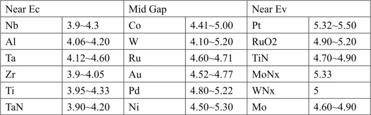
(20) It is also worth to note that the high gate tunneling leakage current is another serious issue when device is scaled 8down. To solve this problem, high-k materials may be used to replace conventional SiO2 gate dielectric. The introduction of high-k materials, however, will lead to a new problem that the thermal stability of conventional poly silicon on high-k is poor. The introduction of metal gates will be expected to provide a turning point [10-13].. In summary, metal gates can provide lower resistivity and eliminate the boron penetration and poly depletion effect. The metal gate technology will play a more important role beyond the 70 nm CMOS technology node.. 1-2 Basic Requirement for Metal Gate The use of metal gate electrodes can possess lower resistivity and eliminate the inherent drawbacks of conventional poly silicon gates such as the boron penetration and poly depletion effect.. First, metal gates must have suitable work function because of gate work function is one of the primary factor to decide the threshold voltage of MOSFET. Not all metals can possess work function suitable for producing a surface channel device with a threshold voltage below 0.3V in magnitude. Table 1-1 lists the work function of some metals[14][15]. Some of them possess a work function suitable to nMOSFETs or pMOSFETs, but the thermal stability of. -3-.
(21) metals such as Al, Ti, and Au are not very good. Those metals interact with gate dielectrics creates some concern. Certain metal gate materials possibly can react with certain high-k dielectric materials. For example, Al can react with HfO2 and forms Al2O3 at the dielectric and metal gate interface then increases effective oxide thickness. However, inert chemicals and thermally stable materials with appropriate work functions are the primary gate materials.. The early approach of metal gate technology employs single metal with work function near the valence band of Si can only produce surface channel pMOSFET, and vice versa. If a single metal is used as the gate electrode of both nMOSFET and pMOSFET, one of them would be able to suffer implantation down to produce buried channel. Counter channel doping can lower the threshold voltage, the channel concentration must be lowered to obtain a low threshold voltage, as shown in Fig.1-2. But after implantation, the buried channel device will be formed, and the short-channel and turn-off characteristics will be degraded. Another approach is use single metal gate with mid-gap work function for both nMOSFET and pMOSFET [16], that can provide symmetrical threshold voltages. The drawbacks are that the threshold voltages would be too large to be applied to low voltage and low power applications, would also be able to suffer implantation down to produce buried channel. Therefore, an approach analogous to the established dual-poly-silicon gate technology, i.e., a dual-metal gate technology, and it would be preferred. For bulk CMOS devices, metals with work functions (Φm) near the silicon conduction and valence band edges, i.e., ~4eV and ~5.1eV, are -4-.
(22) needed for nMOS and pMOS devices, respectively (Fig. 1-3) [17]. It is also worth to note that the values of required metal work functions depend on body thickness[18]. To achieve low and symmetric threshold voltage, the required work functions for n- and p-channel devices will be increased and decreased, respectively, compared to those for bulk devices, as shown in Fig.1-4. Therefore, the required metal work functions would be about 4.4 ~ 4.6 eV and 4.8 ~ 5.0 eV for n- and p-channel devices, respectively. In selecting metal-gate materials for device integration, the metal work function is an important consideration since it directly affects the threshold voltage and the performance of a transistor. The identification of metal-gate materials is a challenging task because metal-gate work functions are observed to be dependent on the underlying gate dielectric [19][20]. The dependence of the gate dielectric material to be due to dipole formation at the interface of the gate electrode and the gate dielectric, as shown in Fig.1-5. When the metal Fermi level Ef,m is above the pinning level, i.e., qφ m < qφ pin,ex , a dipole is created that is charged negatively on the dielectric side (Fig. 1-5(a)). When the metal Fermi level Ef,m is below the extrinsic pinning level, i.e., qφ m > qφ pin,ex , a dipole is created that is charged positively on the dielectric side(Fig. 1-5(b)). For both cases, the interfacial dipole drives the metal Fermi level toward to the pinning level. This model has been particularly successful for metal-dielectric interfaces where there is minimal interfacial reaction [19][20], or where intrinsic states or metal-induced gap states (MIGS) dominate.. -5-.
(23) The resistivity of metal material has been already much lower than that of traditional poly-Si, Table. 1-2 shows the resistivity of several metal materials. But not every metal material is suitable for fabricating metal gate of MOSFET device. For example, Al is chemically active or may react with the gate dielectric. Cu can react easily with other elements and can seriously contaminate SiO2 and Si [21].. 1-3 Reviews of state-of-the-art Metal Gate Technologies Here, we will review some metal gate technologies, such as mid-gap work function of TiN gate, dual work function metal gate using Ti and Mo, dual work function by Ni-Ti interdiffusion, and work function adjustment of the single metal gate by full silicidation.. 1-3-1 Mid-gap Work Function of TiN gate. The early approach of metal gate technology employs single metal with mid-gap work function such as TiN for both nMOSFET and pMOSFET [14], to provide symmetrical threshold voltages. The drawback is that the threshold voltages would be too large for low voltage and low power applications. Counter channel doping can lower the threshold voltage, but the buried channel may be formed. So that the short-channel effect and turn-off. -6-.
(24) characteristics will be degraded. In the view of device performance and scaling, the dual work function technology will be a better choice.. 1-3-2 Dual Work Function Metal Gate Using Ti and Mo An intuitional method for dual work function metal gate technology is using different metal candidates with suitable work function for nMOSFET and pMOSFET ,respectively. In Fig. 1-6, Ti metal gate is used for nMOSFET and Mo metal gate is used for pMOSFET. After blanket deposition, the first layer metal Ti (Φm ~4eV) is removed from the pMOS region and then the second layer metal Mo (Φm ~5eV) is deposited [22]. But this approach will expose the gate dielectric in metal etchant. It will make the effective oxide thickness uncertain, and degrade the gate dielectric reliability.. 1-3-3 Dual Work Function by Ni-Ti interdiffsion A novel dual work function metal gate technology without exposing the gate dielectric in metal etchant was proposed [23-25]. First, a thin Ti (Φm ~3.9eV) layer and Ni (Φm ~5eV) layer were deposited over the entire wafer in sequence. Ni (Φm ~5eV) was then selectively removed from the nMOS region while the pMOS regions were protected by photoresist (Fig. 1-7). Since the low work function metal Ti is the only metal remaining on top of the nMOS, it will clearly determine the -7-.
(25) nMOSFET threshold voltage. A 400℃ anneal was then applied to allow for Ni-Ti interdiffusion in the pMOS region. Due to the high diffusivity of Ni in Ti, this low thermal budget is sufficient to ensure that Ni diffuses through the Ti layer to the dielectric interface. as shown in Fig. 1-8. Doing it in this way will have a lot of shortcomings. It would produce larger leakage current and cause worse thermal stability in pMOS region because of Ti and gate dielectric react during interdiffusion anneal.. 1-3-4 Work Function Adjustment by Fully Silicided Metal-Gate Electrode The self-aligned silicide (SALICIDE) technology has been used in advanced CMOS process [26]. But the gate resistance is still not small enough, because of only partial poly-silicon gate be silicided. Other problems are still unable to avoid, such as poly gate depletion and boron penetration. It can obtain a lot of advantages to extend SALICIDE technology for fully silicided gate, and its low temperature formation is CMOS compatible (Fig.1-9). The MOS capacitors with SiO2 gate dielectric were fabricated on Si substrates. Polysilicon. was. deposited. on. the. gate. dielectric.. For. n+. polysilicon,. in-situ. phosphorous-doping technique during deposition was used. And then boron ions were implanted into undoped polysilicon. Both n+ and p+ polysilicon films underwent the dopant. -8-.
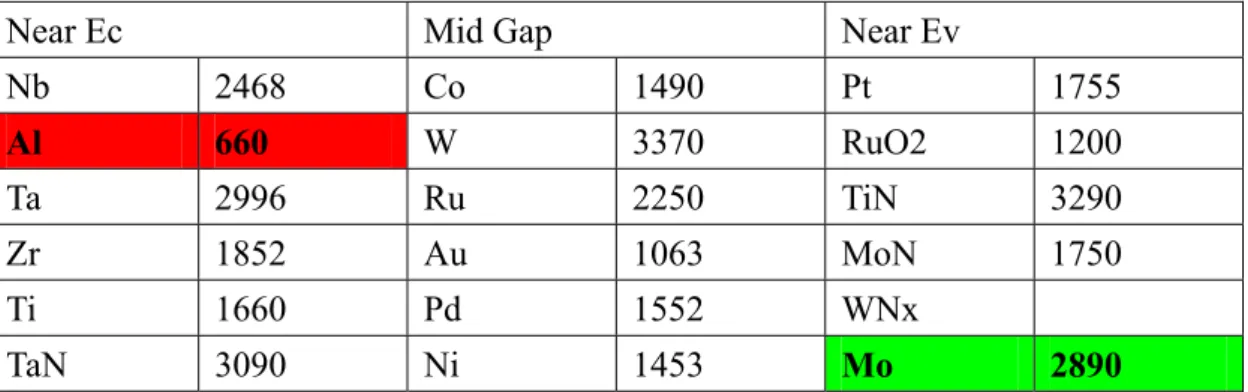
(26) activation anneal. Hafnium was sputtering deposited on poly-silicon. Silicidation was done by furnace annealing. No channel doping was utilized. From electrical results, it is estimated that nMOS work function is ~4.23eV and pMOS ~4.87eV. The change of metal work function may be attributed to As and B piled-up at the gate dielectric interface for nMOSFET and pMOSFET, respectively [27]. The work function is still too large to obtain low threshold voltage for bulk CMOS device, and the channel doping will still be needed for threshold voltage control. Another drawback is that Boron penetration may recur in pMOS region again because of still using boron dopants.. 1-4 Why we chose Molybdenum Silicide ? Molybdenum has high melting point (Table 1-3), low expansion coefficient and low resistivity (Table 1-2). Those are good for MOSFET fabrication process. The thermal stability of molybdenum may reach 900℃ on SiO2 dielectric [28]. The application in other high-k dielectrics may be expect that also has the same thermal stability. The work function of molybdenum on SiO2 dielectric is about 4.69eV [28], and has the wide adjustability(4.6 ~ 4.9eV) that is depending on crystal orientation [29]. Molybdenum has suitable work function on SiO2 dielectric, may use it to fabricate the metal gate of pMOSFET device, and may use it to the dual work function metal gate CMOS process[30][31]. Because the threshold voltage of MOSFET can be affected by the work function of metal gate, therefore we expect to join it Si. -9-.
(27) atoms to form the Mo-silicide and adjust the work function and threshold voltage, make it suitable for nMOSFET device. Fig. 1-10 shows the schematic of CMOS device process flow diagram, using molybdenum silicide gate and pure molybdenum gate for nMOSFET and pMOSFET, respectively.. HfO2 has the suitable permittivity for high-k dielectric of MOSFET device, it did not react with Si substrate and high temperature formation. Beside the work function of Mo-silicide on SiO2 dielectric, the work function and thermal stability of Mo-silicide gate on HfO2 also is a key point which we studies.. 1-5 Organization of the Thesis The thesis is divided into five chapters. In chapter 1, we introduce the evolution of gate candidates and basic requirement for metal gate, we also review some metal gate technologies and discuss their advantages and drawbacks. Midgap work function of TiN, dual work function metal gate using Ti and Mo, dual work function by Ni-Ti interdiffusion and the work function adjustment of the single metal gate by full silicidation. In chapter 2, the detailed process flow will be described involve LOCOS isolation, gate oxide growth, metal gate deposition, electrical characteristics measurement. The method of metal work function extraction will also be addressed. Chapter 3 focuses on electrical characteristics and thermal. - 10 -.
(28) stability of Mo-silicide and pure Mo gate on SiO2 gate dielectric. Different rapid thermal anneal temperature are performed to form Mo-silicide and estimate the thermal stability. Chapter 4 focuses on electrical characteristics and thermal stability of Mo-silicide and pure Mo gate on HfO2 gate dielectric. Different rapid thermal anneal temperature are performed to form Mo-silicide and estimate the thermal stability. Chapter 5 we make a simple conclusion of this thesis.. - 11 -.
(29) Chapter 2 Experiments and Measurements. 2-1 Process Flow of the Molybdenum silicidation Gated Capacitor This experimental step is MOS capacitor fabricating process. All experiments were carried out in National Nano Device Laboratory (NDL). The detailed fabrication process steps are described as follows.. 2-1-1 Molybdenum silicide metal gate with SiO2 dielectric The molybdenum silicide gated capacitors were fabricated on 6-inch n-type (100) 15 - 25 Ω-cm silicon wafers. The process flow is shown in Table 2-1.. First all wafers will engrave the number by Laser Marking System. Particle will be removed after NH4OH + H2O2+ H2O. An initial alignment key was formed at wafer surface for each mask alignment afterward. A wafer with a bare silicon surface was RCA cleaned to remove organic material, metal ions and Native Oxide. A 35 nm oxide was thermally grown in the horizontal furnace at 950 ℃ on the surface. The function of this layer, called a pad - 12 -.
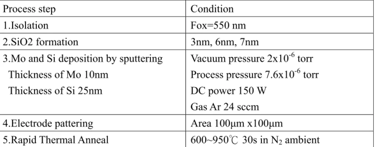
(30) oxide, used to resist stress which produced between silicon surface and silicon nitride. Next, a 150 nm thick layer of LPCVD silicon nitride was deposited at 780 ℃. This layer is to prevent oxygen diffusing to silicon substrate. Silicon nitride was effective in this role because oxygen and water vapor diffused very slowly through it. In addition, the nitride itself oxidized very slowly as the field oxide was grown. In addition, a photoresist pattern is normally used to protect all of the areas where active devices would be formed. After photoresistance coating, the active region of MOSFET was defined by using the G-line Stepper, 435nm ultraviolet. The nitride layer was etched by TEL 5000, and then the photoresist was stripped. After active regions definition, the field oxide 550 nm was thermally grown by means of wet oxidation at 980 ℃. Following field oxidation, the masking layer was removed. Since 20-30 nm of the top of the nitride was converted to SiO2 during the field oxidation, this layer must be etched off first by BOE dipping for 15 seconds. The remaining nitride and pad oxide were then etched. Nitride was removed by H3PO4 at 165 ℃ for 65 minutes and pad oxide was removed by HF. A 35 nm sacrificial oxide was grown at 925 ℃ to remove any dry-etch induced damage or unwanted nitride. And then, using the HF solution removed the sacrificial oxide.. Before starting to grow gate oxide, native Oxide have to be removed by dilud HF (HF:H2O=1:50) to accurate control gate oxide thickness, and avoids the electrical weaken which because of Extra gate oxide thickness. After RCA clean, gate oxide was thermally grown by dry oxidation using the vertical furnace at 800 ℃. In order to eliminate the - 13 -.
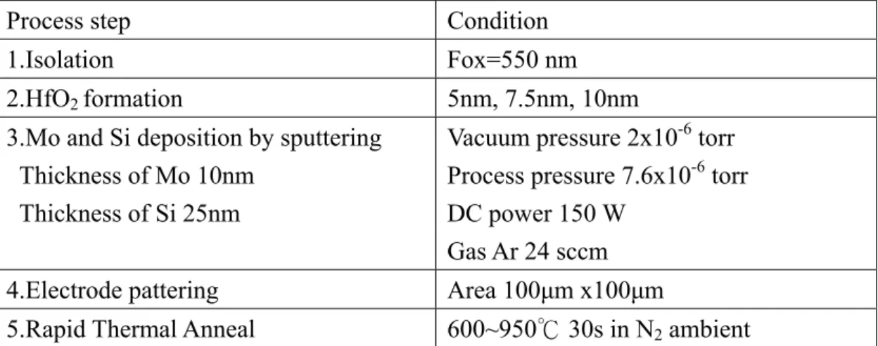
(31) contribution of fixed charge, three different oxide thicknesses (3 nm, 6 nm, and 8 nm) were deposited.. After the growth of gate oxide, Molybdenum and silicon films were deposited in a sputtering system to a thickness of 10nm and 25nm, respectively. Neither substrate bias nor heating was intentionally applied to the deposition system. The process chamber was pumped down to 2x10⁻⁷ torr before the films were deposited. The pressure of the process chamber was kept at 7.6x 10⁻³ torr during deposition. The DC power was set to 150 W. the Ar gas flow was set to 24 sccm. The gate electrode was then capped by 20 nm TiN. The conventional photo lithography process was then used to define an gate region with an area of 100x100 µm2. The gate electrodes were then patterned by reactive ion etching using Cl2 based chemistry. Unpatterned sample with TiN(20 nm)/Si(25 nm)/Mo(10 nm) were also prepared for material analysis.. In order to form the Mo-silicide and examine thermal stability of gate dielectric, all samples were then subjected to different rapid thermal anneal temperature from 600 ℃ to 950 ℃ for 30s.. 2-1-2 Molybdenum silicide metal gate with HfO2 High-k dielectric The process flow of the Ti/Si/Mo/HfO2/Si-Sub MOS capacitor structure fabrication, as. - 14 -.
(32) shown in Fig. 2-1, resembles that of the Ti/Si/Mo/SiO2/Si-Sub MOS capacitor, except that thermal SiO2 was replaced by MOCVD HfO2. The process flow chart is shown in Table 2-2. After LOCOS formation, HfO2 with different thickness were deposited by atomic vapor deposition in an AIXTRON Tricent system at a substrate temperature of 500 ℃. The MOCVD system was designed for 8-inch wafers, so a 6-inch quartz was used as wafer carrier for film deposition. The same process flow was then carried out to complete Ti/Si/Mo/HfO2/Si-Sub MOS capacitor.. 2-2 Measure techniques and material analysis In this section, we introduce some instruments of material analysis and measure techniques of electrical property. The instruments of material analysis include Ellipsometer and X-ray Diffraction Analysis (XRD). In the aspect of electrical properties, we use Keithley 4200-SCS to measure the C-V curves of MOS capacitors.. 2-2-1. Physical Thickness Measurement of Ultra-Thin Gate Oxide using. Ellipsometer An ellipsometer enables to measure the refractive index and the thickness of semi-transparent thin films. The instrument relies on the fact that the reflection at a dielectric interface depends on the polarization of the light while the transmission of light through a. - 15 -.
(33) transparent layer changes the phase of the incoming wave depending on the refractive index of the material. An ellipsometer can be used to measure layers as thin as 1 nm up to layers with several microns thick. Applications include the accurate thickness measurement of thin films, the identification of materials and thin layers and the characterization of surfaces.. 2-2-2. Capacitance-Voltage Measurement using KEITHLEY 4200. The Keithley 4200-SCS has built-in support for the control of external C-V analyzers. It supports both the Keithley 590 C-V Analyzer and the HP4284A Precision LCR meter, controlling them via Keithley User Library Tool (KULT) user modules through Keithley Interactive Test Environment (KITE) User Test Modules (UTMs).. 2-3. Flat-Band Voltage Extraction In the strong accumulation region, the MOS capacitor acts like a parallel-plate capacitor,. and the oxide thickness may be calculated from COX and the gate area using the following equation :. tox =. εoxA ……………………………………..(1) Cox(1x10 −19 ). - 16 -.
(34) where tOX is the oxide thickness (nm), A is the gate area (cm2), εox is the permittivity of the oxide material (F/cm), and COX is the oxide capacitance (pF). Oxide thickness calculations based on C-V measurements can be very precise, unless improperly extracted. Oxide thickness must be extracted from the strong accumulation region, where the capacitance measured truly reflects the oxide capacitance. Adding a flat-band voltage (VFB) on gate will result in the disappearance of band bending. At this point, known as the flat-band condition, the semiconductor band becomes flat. And the surface potential is zero (with the reference potential being taken as the bulk potential deep in the semiconductor). Flat-band voltage and its shift are widely used to extract other device parameters, such as oxide charges. We can identify VFB from the C-V curve. First, we can estimate the flat-band capacitor from C-V data, and then find out the flat-band voltage VFB. In the C-V theory, the flat-band capacitance can be expressed as following:. CFB =. εox kT εSi εox ) tox + ( ) ( )( q qNd εSi. ……………………………………..(2). where tox is the effective oxide thickness, Eq.(1), Nd is the substrate doping concentration , and εox and εSi are the dielectric constant of oxide and silicon substrate, respectively. According to the flat-band capacitance, we can extract the flat-band voltage from the C-V - 17 -.
(35) measurement.. 2-4. Extracting Work Function From effective oxide thickness and flat-band voltage, the metal gate work function can. be extracted. Following is the expression of flat-band voltage:. VFB = Φ ms −. Q ss Qss t ox ……………………………………..(3) = Φ ms − C ox ε ox. Φ m = Φ ms + Φ s …………………………………………………………..…..(4). where Qss is the density of fixed oxide charges, Φ m is the metal work function and Φs is the Fermi level of silicon substrate. In order to eliminate the contribution of fixed oxide charge from the work function, C-V measurement on several oxide thickness were used to generate a VFB vs. EOT plot. The y-intercept of this plot indicates the Φms value, then the work function of metal gate can be extracted by Eq.(4). Since Qss must be constant in order to obtain meaningful values of Φms, we have prepared three kinds of different thickness of gate oxide on the same wafer to ensure that Qss is the same.. - 18 -.
(36) Chapter 3 Molybdenum Silicide Gate Electrode on SiO2 Dielectric. 3-1. Introduction Metal gate electrodes have been investigated to replace poly-Si to solve problems such as. poly depletion effects and boron penetration for future CMOS devices. Several approaches for dual metal gate process such as metal interdiffusion gate and nitrogen implantation into a single metal have recently been proposed [22-25][30]. However, most of thermally stable metals suitable for CMOS process have work functions near mid-gap or the valance band of silicon. Since the metals with low work functions are inherently unstable and reactive, searching a suitable metal for nMOSFET gate electrode with thermal stability compatible with CMOS front-end process remains a challenge. Recently, fully silicided (FUSI) metal silicides such as NiSi and CoSi for dual metal gates have drawn considerable attention due to its CMOS compatibility and no process-induced damage to the gate dielectric [31]–[34]. Unfortunately, boron penetration may be suffered at the pMOSFET if boron implantation is used to tuning work function of the electrode of pMOSFET device. In this work, we demonstrate for the first time that FUSI Mo-silicide with a work. - 19 -.
(37) function of 4.008 eV and excellent thermal stability up to 950 ℃ can be used as a gate electrode material for nMOSFETs. In addition, Mo can possess high work function on SiO2 dielectric, suitable for the gate electrode of pMOSFET [29]. The use of Mo for pMOSFET can also eliminate the boron penetration, and provide excellent thermal stability up to 950 ℃. Here, we propose an new approach to fabricate CMOS device with a suitable work function and excellent thermal stability, as shown in Fig. 1-10.. 3-2. Experiment The MOS capacitors with different thickness of SiO2 gate dielectric (30, 60, 80 nm) were. fabricated on 6-in. n-type (100) Si substrates. Molybdenum with a thickness of 10 nm and amorphous silicon with a thickness of 25 nm were deposited on the gate dielectric using a sputtering system under an argon ambient with a base pressure of 7.6 mtorr. Some sample were then subjected to As ion implantation with a dosage of 1x1015 cm-2 ~ 5x1015 cm-2. About a 20-nm-thick titanium nitride capping layer was subsequently deposited on top of gate electrode. The titanium nitride capping layer can prevent amorphous silicon from being oxidized during silicidation. Gate electrodes of all samples were etched in a Cl2-based helicon-type plasma etcher, followed by photoresist stripping in a down-stream O2 plasma asher. Silicidation was done by rapid thermal annealing (RTA) at different temperatures ranging from 600 ℃ to 800 ℃ for 30 s. For the evaluation of thermal stability of the. - 20 -.
(38) Mo-silicide, the samples were annealed in a RTA chamber at 950 ℃ for 30 s.. 3-3. Results and Discussion In order to know the condition of forming silicidation with molybdenum and silicon. stack structure, we fabricated MOS capacitors with different thickness of α-Si layer. C-V measurements shows that for sample with 15 nm of silicon layer, the flat-band voltage remains unchanged indicating that molybdenum silicide is sufficiently far from the interface of gate dielectric and not to effect capacitor’s electrical property. For 25 nm thick silicon layer, flat-band voltage progressively shift tower to lower voltage in nMOS capacitor, as shown in Fig. 3-1. Fig. 3-2 shows the work function extraction of molybdenum silicide metal gate with SiO2 dielectric. In order to decouple the effect of fixed charge, C-V measurements on MOS capacitors with varying oxide thickness were used to generate a flat-band voltage vs. equivalent oxide thickness plot. The work function can be extracted from the y-intercept of this curve. All conditions exhibited linear behavior from which work function could be extracted. The work function of as-deposited gate electrode is 4.781 eV. After rapid thermal anneal for 700 ℃ 30s, the work function of gate electrode have only a negligible variation. The work function of molybdenum and silicon stacked gate after 700 ℃ RTA is not the same as the work function of pure molybdenum gate (4.931 eV, as shown following). This is may. - 21 -.
(39) be silicon ions diffused to dielectric interface during sputtering, cause Mo and Si mixture substance at this time. Therefore, the work function of MOS capacitance has been shift to near mid-gap region of silicon. As temperature increase to 800 ℃, the work function of gate electrode has a noticeable shift from 4.775 eV to 4.389 eV. Fig. 3-3 shows the extracted work function versus rapid thermal anneal temperature. We can see from this picture, the work function violent decline obviously that is may be silicon and molybdenum mixture substance has already been formed molybdenum silicde during 800 ℃ rapid thermal anneal. Fig. 3-4 shows the sheet resistance versus the annealing temperature. Sheet resistance was measured without stripping the titanium nitride capping layer. As molybdenum and silicon just been deposited on gate dielectric, the sheet resistance of gate electrode is seems too large that is due to amorphous silicon has worse electric conductivity. After 800 ℃ rapid thermal anneal, the Mo-sisicide was been formed and sheet resistance of gate electrode was decrease to about 76 Ω/□. The thermal stability of Mo-silicide gate is further investigated by RTA up to 950 ℃ for 30s, which is the temperature required for source/drain implantation annealing. In our experiments, the TiN film successfully played a role of capping layer, Fig. 3-4 showing no degradation of sheet resistance even after a high temperature annealing at 950 ℃. After annealing at 950 ℃, the sheet resistance of 20-nm-thick TiN capped Mo-silicide stack gate was measured to be about 79 ohms/square. Further reduction of sheet resistance can be. - 22 -.
(40) achieved by increasing the TiN thickness. The EOT of TiN capped Mo-silicide gated MOS capacitors show negligible variation even after annealing at 950 ℃, as shown in Fig. 3-5. Gate oxide leakage current shown in Fig. 3-6 also shows no meaningful difference between 800 ℃ and 950 ℃ rapid thermal annealing. Gate leakage become smaller and smaller with the increase of temperature, and tend to steady when temperature increase to 950 ℃. Process quality was demonstrated in Fig. 3-7, hysteresis of Mo-silicide gated MOS capacitor with 950 ℃ Rapid thermal anneal still exhibits negligible. The work function of undoped Mo-silicide gate electrode is 4.389 eV. That is just suitable for FinFET and ultra-thin body (UTB) MOSFET device. Therefore, we use As ion implantation to dope the gate electrode and observe the change of work function. Silicidation was performed under the same FUSI condition. Fig. 3-8 plots the flat-band voltage of Mo-silicided devices versus the effect oxide thickness (EOT) for As- and un-doped Mo-silicide gate electrode, that was undergo 800 ℃ 30s RTA and Mo-silicide has been formed. The extracted work function values are summarized in Fig. 3-9. Comparing the work function of doped and undoped Mo-silicide, it becomes evident that the arsenic dopants strongly affect the work function of Mo-silicides. That may be attributed to the As pile-up at the Mo-silicide and SiO2 interface changing the electrical property of MOS capacitor. Similar As pile-up has been reported in FUSI gates[35][36]. The work function difference between As-doped and undoped Mo-silicide can be at least up to 0.379 eV, and the work function of. - 23 -.
(41) Mo-silicided gate with As 5x1015 cm-2 becomes 4.001 eV, that is suitable for bulk nMOSFET device. The thermal stability of Mo-silicide gate with 5x1015 cm-2 As-implant is further investigated by RTA up to 950 ℃. The EOT of Mo-silicide gated MOS capacitors with 5x1015 cm-2 As-implant show negligible change even after annealing at 950 ℃, as shown in Fig. 3-10. Based on these results, Mo-silicide gate with 5x1015 cm-2 As implanted during 800 ℃ for 30s RTA may chose for bulk nMOSFET device fabrication. Fig. 3-11 shows the flat-band voltage of pure Mo gated MOS capacitor as a function of the oxide thickness. The work function of pure Molybdenum gate after 950 ℃ rapid thermal anneal is about 4.931 eV, that is very close to the reported result [29]. Fig. 3-12 shows. the. hysteresis of pure Mo gated MOS capacitor with 950 ℃ rapid thermal anneal still exhibits negligible variation. Therefore, pure Mo gate may chose for pMOSFET device fabrication. We proposed and demonstrated fully silicide Mo-silicide with 5x1015 cm-2 As implanted as a metal-gate material for nMOSFETs (work function 4.001 eV) and pure Mo as a metal-gate material for pMOSFETs (work function 4.931 eV). Those were compatible with CMOS processing. Negligible change in work function and EOT are observed even after annealed at 950 ℃, demonstrating its excellent thermal stability. Therefore, Mo-silicide and pure Mo gate electrode is the promising candidate for dual-metal work function CMOS. - 24 -.
(42) device.. - 25 -.
(43) Chapter 4 Molybdenum Silicide Gate Electrode on HfO2 Dielectric. 4-1 Introduction For the sub-micron CMOS device, silicon dioxide gate dielectric will suffer large gate leakage current. Therefore, a lot of high dielectric constant (high-k) materials like Al2O3, ZrO2 and HfO2 have been widely studied to replace the silicon dioxide to reduce gate leakage. Unfortunately, poly silicon gate electrode was easily interact with high-k dielectric. And some other issues such as poly gate depletion, boron penetration and high resistivity have been suggested that using metal gate to replace poly silicon gate. However, in order to achieve suitable threshold voltage for n and pMOSFETs, the work function of metal gate near band-edge of silicon is necessary. In this chapter, we will use the same structure with chapter 3, but replace the SiO2 gate dielectric with HfO2 in order to reduce gate leakage current and observe the change of the Mo-silicided gate work function on HfO2 high-k dielectric. The thermal stability of Mo-silicide gate on HfO2 high-k dielectric is also investigated by RTA up to 950 ℃.. - 26 -.
(44) 4-2 Experiment MOS capacitors were fabricated on 6-in. n-type silicon wafers with conventional LOCOS isolation process. The different thickness of MOCVD HfO2 gate dielectric (30, 60, 80 nm) were deposited as gate dielectric. Molybdenum with a thickness of 10 nm and amorphous silicon with a thickness of 25 nm were deposited using a sputtering system in an argon ambient with a base pressure of 7.6 mtorr. Some samples were implanted by As with a dosage of 5x1015 cm-2. About A 20-nm-thick titanium nitride capping layer was subsequently deposited on top of gate electrode. Gate electrodes of all samples were etched in a Cl2-based helicon-type plasma etcher, followed by photoresist stripping in a down-stream O2 plasma asher. Silicidation was done by rapid thermal annealing (RTA) at different temperatures ranging from 600 ℃ to 800 ℃ for 30s. For the evaluation of thermal stability of the Mo-silicide, the samples were annealed in a RTA chamber at 950 ℃ for 30 s.. 4-3 Results and Discussion Fig. 4-1 shows the extracted work function versus rapid thermal anneal temperature. The work function of Mo-silicided gate after 600 ℃ and 700 ℃ is about 4.813 eV and 4.792 eV, respectively. The work function of gate electrode have only a negligible variation. After 800 ℃ rapid thermal anneal, The work function of Mo-silicide shift to 4.34 eV. This situation is quite similar to using Mo-silicided gate electrode with SiO2 gate dielectric, and has not seen obvious fermi pinning effect. This may be due to fermi pinning level very close to 4.34 eV.. - 27 -.
(45) Fig. 4-2 shows the variation of equivalent oxide thickness of FUSI molybdenum silicide gated MOS capacitors on HfO2 versus different temperatures. Excellent thermal stability up to 950 ℃ is observed. The Mo-silicided gate is quite stable on hafnium dioxide. The work function of undoped Mo-silicide gate electrode on HfO2 is about 4.34 eV. That is just suitable for FinFET and ultra-thin body (UTB) MOSFET device. Therefore, we use As ion implantation to dope the gate electrode and observe the change of work function. Silicidation was performed under the same FUSI condition in chapter 3 for 5x1015 cm-2 As-doped samples. The extracted work function values are summarized in Fig. 4-3 after 800 ℃ RTA. Comparing the work function of doped and undoped Mo-silicide, it becomes evident that the arsenic dopants strongly affect the work function of formed Mo-silicides. That may be attributed to the As pile-up at the Mo-silicide and HfO2 dielectric interface changing the electrical property of MOS capacitor. The work function difference between As-doped and undoped Mo-silicide with HfO2 gate dielectric can be at least up to 0.363 eV, and the work function of Mo-silicided gate with As 5x1015 cm-2 on HfO2 dielectric becomes 4.16 eV, that is suitable for bulk nMOSFET device. The thermal stability of Mo-silicide gate with 5x1015 cm-2 As-implant is further investigated by RTA up to 950 ℃. The equivalent oxide thickness of Mo-silicide gated MOS capacitors with 5x1015 cm-2 As-implant on HfO2 shows negligible change even after annealing at 950 ℃, as shown in Fig. 4-4.. - 28 -.
(46) Based on these results, Mo-silicide gate with 5x1015 cm-2 As implanted on HfO2 gate dielectric during 800 ℃ 30s RTA may chose for bulk nMOSFET device fabrication. pMOSFET device with HfO2 gate dielectric also fabricated and discussed. The work function of pure Molybdenum gate with HfO2 gate dielectric after 950 ℃ rapid thermal anneal is about 4.906 eV. The C-V curve of pure Molybdenum gated MOS capacitor with HfO2 gate dielectric was shows in Fig. 4-5, and Fig. 4-6 shows the oxide quality leakage current characteristic. The leakage current of MOS capacitor with high-k HfO2 dielectric is smaller than that of MOS capacitor with SiO2 gate dielectric. Using HfO2 as gate oxide can make the gate oxide leakage current improve about 2 orders than SiO2. Therefore, pure Mo gated MOSFET device with HfO2 gate dielectric may chose for pMOSFET device fabrication. We proposed and demonstrated fully silicided Mo-silicide with 5x1015 cm-2 As implanted as a metal-gate material for nMOSFETs (work function 4.16 eV) and pure Mo as a metal-gate material for pMOSFETs (work function 4.906 eV) on HfO2 high-k gate dielectric, those were compatible with CMOS processing. Negligible change in flat-band voltage and equivalent oxide thickness are observed even after annealed at 950 ℃, demonstrating its excellent thermal stability. The gate oxide leakage current of CMOS device can also get suitable improvement than SiO2. Therefore, Mo-silicide for nMOSFET with pure Mo for pMOSFET is the promising candidate for dual-metal CMOS process with HfO2 High-k dielectric.. - 29 -.
(47) Chapter 5 Conclusion. This thesis investigated the work function adjustability of fully Mo-silicide films and the thermal stability of gate dielectric and equivalent oxide thickness of Mo-silicide MOS devices. The molybdenum and amorphous silicon were deposited by sputtering system in Ar ambient. Samples with metal/SiO2/Si-sub MOS structures annealed at different temperature in RTA (rapid thermal anneal) system in N2 ambient were used to analyze the thermal stability of the flat-band voltage and equivalent oxide thickness. Using the same process condition, the molybdenum and amorphous silicon were deposited on HfO2 high-k Dielectric that deposited by MOCVD system. Investigating the work function adjustability and thermal stability of flat-band voltage and equivalent oxide thickness of MoSix/High-k/Si-sub structures. The work function of the Molybdenum silicide on SiO2 dielectric decreased from 4.78 eV to 4.39 eV as anneal temperature increased to 800 ℃ 30s. And on the aspect of the molybdenum silicidation on HfO2 high-k dielectric, the work function was decrease from 4.81 eV to 4.34 eV as anneal temperature increase to 800 ℃ 30s. The work function of the molybdenum silicide has not seen obvious fermi pinning effect. This may be due to fermi pinning level very close to 4.34 eV. After that, using arsenic ion implantation to add arsenic to. - 30 -.
(48) gate of MOS structure, to cause the work function of the gate on SiO2 dielectric decrease to 4.001 eV. And the work function of the gate on HfO2 high-k dielectric decrease to 4.16 eV. To investigate the thermal stability of gate oxide and equivalent oxide thickness, the samples were annealed by RTA system at 600 ℃、700 ℃、800 ℃ and 950 ℃, and found that no matter what metal silicide on SiO2 or HfO2 dielectric, the deviation of the metal work function and equivalent oxide thickness annealed among 800 ℃ and 950 ℃ can be neglect. Suggesting the molybdenum silicide metal gate can replace the traditional n+ poly-Si gate. The work function of pure Mo on SiO2 and HfO2 is about 4.931 eV and 4.906 eV, respectively. That is very close to the valance band of silicon. The deviation of the metal work function and equivalent oxide thickness annealed up to 950 ℃ can be neglect. Based on these results, Mo-silicide gate for nMOS and pure Mo gate for pMOS may chose for CMOS device fabrication.. - 31 -.
(49) Reference : [1] S.M Sze “Semiconductor Device Physics and Technology” ch.5, p.41, John Wiley and Sons [2] Pfiester, J.R.; Baker, F.K.; Mele, T.C.; Tseng, H.-H.; Tobin, P.J.; Hayden, J.D.; Miller, J.W.; Gunderson, C.D.; Parrillo, L.C.; “The effects of boron penetration on p+ polysilicon gated PMOS devices” Electron Devices, IEEE Transactions on Volume 37, Issue 8, Aug. 1990 Page(s):1842 – 1851 [3] Morimoto, T.; Momose, H.S.; Ozawa, Y.; Yamabe, K.; Iwai, H.; “Effects of boron penetration and resultant limitations in ultra thin pure-oxide and nitrided-oxide gate-films” Electron Devices Meeting, 1990. Technical Digest., International 9-12 Dec. 1990 Page(s):429 – 432 [4] Ming-Yin Hao; Nayak, D.; Rakkit, R.; “Impact of boron penetration at P+-poly/gate oxide interface on deep-submicron device reliability for dual-gate CMOS technologies” Electron Device Letters, IEEE Volume 18, Issue 5, May 1997 Page(s):215 – 217 [5] Min Cao; Vande Voorde, P.; Cox, M.; Greene, W.; “Boron diffusion and penetration in ultrathin oxide with poly-Si gate” Electron Device Letters, IEEE Volume 19, Issue 8, Aug. 1998 Page(s):291 – 293 [6] Bauer, A.J.; Mayer, P.; Frey, L.; Haublein, V.; Ryssel, H.; “Implantation of nitrogen into polysilicon to suppress boron penetration through the gate oxide” Ion Implantation Technology Proceedings, 1998 International Conference on Volume 1, 22-26 June 1998 Page(s):30 - 33 vol.1 [7] Kuroi, T.; Hamaguchi, T.; Shirahata, M.; Okumura, Y.; Kawasaki, Y.; Inuishi, M.; Tsubouchi, N.; “Novel NICE (nitrogen implantation into CMOS gate electrode and source-drain) structure for high reliability and high performance 0.25 µm dual gate CMOS” Electron Devices Meeting, 1993. Technical Digest., International 5-8 Dec. 1993 Page(s):325 – 328 [8] Yung Hao Lin; Chao Sung Lai; Chung Len Lee; Tan Fu Lei; Tien Sheng Chao; “Nitridization of the stacked poly-Si gate to suppress the boron penetration in pMOS” Electron Devices, IEEE Transactions on Volume 43, Issue 7, July 1996 Page(s):1161 – 1165 - 32 -.
(50) [9] Tuinhout, H.P.; Montree, A.H.; Schmitz, J.; Stolk, P.A. “Effects of gate depletion and boron penetration on matching of deep submicron CMOS transistors” Electron Devices Meeting, 1997. Technical Digest., International 7-10 Dec. 1997 Page(s):631 – 634 [10] H. F. Luan, B. Z. Wu, L.G. Kang, B. y. Kim, R. Vrtis, D. Roberts, and D. L. Kwong,,”Ultra thin high quality Ta2O5 gate dielectric prepared by in-situ rapid thermal processing,” IEDM Tech. Dig. Pp.609-612, 1998 [11] C. H. Lee, H. F. Luan, W. P. Bai, S. J. Lee, T. S. Jeon, Y. Senzaki, D. Roberts, and D. L. Kwong, “MOS characteristics of ultra thin rapid thermal CVD ZrO2 and Zr silicate gate dielectrics,” IEDM Tech. Dig. pp.27-30, 2000. [12] Y. C. Yeo, P. Ranade, Q. Lu, R. Lin, T. -J. King, C. Hu, ”Effects of High-k Gate Dielectric Materials on Metal and Silicon Gate Workfunction,” IEEE Electron Device Lett., vol. 23, pp.342-344, 2002 [13] Cheng, B.; Cao, M.; Rao, R.; Inani, A.; Vande Voorde, P.; Greene, W.M.; Stork, J.M.C.; Zhiping Yu; Zeitzoff, P.M.; Woo, J.C.S.; “The impact of high-κ gate dielectrics and metal gate electrodes on sub-100 nm MOSFETs” Electron Devices, IEEE Transactions on Volume 46, Issue 7, July 1999 Page(s):1537 – 1544 [14] Maiti, B.; Tobin, P.J.; Hobbs, C.; Hegde, R.I.; Huang, F.; O'Meara, D.L.; Jovanovic, D.; Mendicino, M.; Chen, J.; Connelly, D.; Adetutu, O.; Mogab, J.; Candelaria, J.; La, L.B.; “PVD TiN metal gate MOSFETs on bulk silicon and fully depleted silicon-on-insulator (FDSOI) substrates for deep sub-quarter micron CMOS technology” Electron Devices Meeting, 1998. IEDM '98 Technical Digest., International 6-9 Dec. 1998 Page(s):781 – 784 [15] Heuss, G.; Misra, V.; “Electrical properties of RuO/sub 2/ gate electrodes for dual metal gate Si-CMOS” Electron Device Letters, IEEE Volume 21, Issue 12, Dec. 2000 Page(s):593 – 595 [16] Maiti, B.; Tobin, P.J.; Hobbs, C.; Hegde, R.I.; Huang, F.; O'Meara, D.L.; Jovanovic, D.; Mendicino, M.; Chen, J.; Connelly, D.; Adetutu, O.; Mogab, J.; Candelaria, J.; La, L.B.; “PVD TiN metal gate MOSFETs on bulk silicon and fully depleted silicon-on-insulator (FDSOI) substrates for deep sub-quarter micron CMOS technology” Electron Devices Meeting, 1998. IEDM '98 Technical Digest., International 6-9 Dec. 1998 Page(s):781 – 784 - 33 -.
(51) [17] De, Indranil; Johri, Deepak; Srivastava, Anadi; Osburn, C.M. “Impact of gate workfunction on device performance at the 50 nm technology node” Solid-State-Electronics, Volume 44, Issue: 6, 2000, pp.1077-1080 [18] Adan, A.O.; Higashi, K.; Fukushima, Y.; “Analytical threshold voltage model for ultrathin SOI MOSFETs including short-channel and floating-body effects” Electron Devices, IEEE Transactions on Volume 46, Issue 4, April 1999 Page(s):729 - 737 [19] Y.-C. Yeo, P. Ranade, T.-J. King, and C. Hu, “Effects of high-k gate-dielectric materials on metal and silicon gate workfunctions,” IEEE Electron Device Lett., vol. 23, pp. 342–344, June 2002 [20] Y.-C. Yeo, T.-J. King, and C. Hu, “metal-dielectric band alignment and its implications for metal gate complementary metal–oxide-semiconductor technology,” J. Appl. Phys., vol. 92, pp. 7266–7271, 2002 [21] J. O. Olowolafe, C. J. Mogab, R. B. Gregory, and M. Kottke “Interdiffusions in Cu/reactive-ion-sputtered TiN, Cu/chemical-vapor-deposited TiN, Cu/TaN, and TaN/Cu/TaN thin-film structures: Low temperature diffusion analyses” J. Appl. Phys., November 1, 1992, Issue 9, pp. 4099-4103, 1992 [22] Yee-Chia Yeo; Qiang Lu; Ranade, P.; Takeuchi, H.; Yang, K.J.; Polishchuk, I.; Tsu-Jae King; Chenming Hu; Song, S.C.; Luan, H.F.; Dim-Lee Kwong; “Dual-metal gate CMOS technology with ultrathin silicon nitride gate dielectric” Electron Device Letters, IEEE Volume 22, Issue 5, May 2001 Page(s):227 - 229 [23] Polishchuk, I.; Ranade, P.; Tsu-Jae King; Chenming Hu; “Dual work function metal gate CMOS technology using metal interdiffusion” Electron Device Letters, IEEE Volume 22, Issue 9, Sept. 2001 Page(s):444 - 446 [24] Polishchuk, I.; Ranade, P.; King, T.-J.; Chenming Hu; “Dual work function metal gate CMOS transistors by Ni-Ti interdiffusion” Electron Device Letters, IEEE Volume 23, Issue 4, April 2002 Page(s):200 – 202 [25] Polishchuk, I.; Ranade, P.; Tsu-Jae King; Chenming Hu; “Dual work function metal gate CMOS transistors fabricated by Ni-Ti interdiffusion” Semiconductor Device Research Symposium, 2001 International 5-7 Dec. 2001 Page(s):411 - 414 - 34 -.
(52) [26] Morimoto, T.; Momose, H.S.; Iinuma, T.; Kunishima, I.; Suguro, K.; Okana, H.; Katakabe, I.; Nakajima, H.; Tsuchiaki, M.; Ono, M.; Katsumata, Y.; Iwai, H.; “A NiSi salicide technology for advanced logic devices” Electron Devices Meeting, 1991. Technical Digest., International 8-11 Dec. 1991 Page(s):653 - 656 [27] Chang Seo Park; Byung Jin Cho; Dim-Lee Kwong; “Thermally stable fully silicided Hf-silicide metal-gate electrode” Electron Device Letters, IEEE Volume 25, Issue 6, June 2004 Page(s):372 - 374 [28] Kwasnick, R.F.; Kaminsky, E.B.; Frank, P.A.; Franz, G.A.; Saia, R.J.; Polasko, K.J.; Gorczya, T.B.; “An investigation of a molybdenum gate for submicrometer CMOS” Electron Devices, IEEE Transactions on Volume 35, Issue 9, Sept. 1988 Page(s):1432 - 1438 [29] Hideaki Matsuhashi and Satoshi Nishikawa; “Optimum Electrode Materials for Ta2O5 Capacitors for High- and Low-Temperature Processes” Jpn. J. Appl. Phys. Vol.33(1994) pp.1293-1297 [30] Qiang Lu; Lin, R.; Ranade, P.; Yee Chia Yeo; Xiaofan Meng; Takeuchi, H.; Tsu-Jae King; Chenming Hu; Hongfa Luan; Songjoo Lee; Weiping Bai; Choong-Ho Lee; Dim-Lee Kwong; Xin Guo; Xiewen Wang; Tso-Ping Ma; “Molybdenum metal gate MOS technology for post-SiO2 gate dielectrics” Electron Devices Meeting, 2000. IEDM Technical Digest. International 10-13 Dec. 2000 Page(s):641 – 644 [31] Pushkar Ranade, Yee-Chia Yeo, Qiang Lu, Hideki Takeuchi, Tsu-Jae King, and Chenming Hu; “Molybdenum as a Gate Electrode for Deep Sub-Micron CMOS Technology ” MRS Spring Meeting Proceedings, 2000 Symposium C3.2, Volume 611 [32] Maszara, W.P.; Krivokapic, Z.; King, P.; Goo, J.-S.; Lin, M.-R.; “Transistors with dual work function metal gates by single full silicidation (FUSI) of polysilicon gates” [33] Kedzierski, J.; Nowak, E.; Kanarsky, T.; Zhang, Y.; Boyd, D.; Carruthers, R.; Cabral, C.; Amos, R.; Lavoie, C.; Roy, R.; Newbury, J.; Sullivan, E.; Benedict, J.; Saunders, P.; Wong, K.; Canaperi, D.; Krishnan, M.; Lee, K.-L.; Rainey, B.A.; Fried, D.; Cottrell, P.; Wong, H.-S.P.; Ieong, M.; Haensch, W.; “Metal-gate FinFET and fully-depleted SOI devices using total gate silicidation” Electron Devices Meeting, 2002. IEDM '02. Digest. International 8-11 Dec. 2002 Page(s):247 - 250 [34] Krivokapic, Z.; Maszara, W.; Achutan, K.; King, P.; Gray, J.; Sidorow, M.; Zhao, E.; - 35 -.
(53) Zhang, J.; Chan, J.; Marathe, A.; Lin, M.-R.; “Nickel silicide metal gate FDSOI devices with improved gate oxide leakage” Electron Devices Meeting, 2002. IEDM '02. Digest. International 8-11 Dec. 2002 Page(s):271 – 274 [35] Maszara, W.P.; Krivokapic, Z.; King, P.; Goo, J.-S.; Lin, M.-R.; “Transistors with dual work function metal gates by single full silicidation (FUSI) of polysilicon gates” Electron Devices Meeting, 2002. IEDM '02. Digest. International 8-11 Dec. 2002 Page(s):367 - 370 [36] Sim, J.H.; Wen, H.C.; Lu, J.P.; Kwong, D.L.; “Dual work function metal gates using full nickel silicidation of doped poly-Si” Electron Device Letters, IEEE Volume 24, Issue 10, Oct. 2003 Page(s):631 - 633. - 36 -.
(54) Near Ec. Mid Gap. Near Ev. Nb. 3.9~4.3. Co. 4.41~5.00. Pt. 5.32~5.50. Al. 4.06~4.20. W. 4.10~5.20. RuO2. 4.90~5.20. Ta. 4.12~4.60. Ru. 4.60~4.71. TiN. 4.70~4.90. Zr. 3.9~4.05. Au. 4.52~4.77. MoNx. 5.33. Ti. 3.95~4.33. Pd. 4.80~5.22. WNx. 5. TaN. 3.90~4.20. Ni. 4.50~5.30. Mo. 4.60~4.90. Table 1-1 The work function of some metals reported in literatures.. - 37 -.
(55) Near Ec. Mid Gap. Near Ev. Nb. 15. Co. 6.86. Pt. Al. 2.65. W. 5.48. RuO2. Ta. 13. Ru. 7.1. TiN. >100. Zr. 42. Au. 2.4. MoNx. >100. Ti. 40. Pd. 10. WNx. >100. TaN. 225. Ni. 6.9. Mo. 4.76. Poly-Si(B). >1000. Poly-Si(As) >1000. 10.5. Table 1-2 The risistivity (µΩ-cm) of some metals reported in literatures.. - 38 -.
(56) Near Ec. Mid Gap. Near Ev. Nb. 2468. Co. 1490. Pt. 1755. Al. 660. W. 3370. RuO2. 1200. Ta. 2996. Ru. 2250. TiN. 3290. Zr. 1852. Au. 1063. MoN. 1750. Ti. 1660. Pd. 1552. WNx. TaN. 3090. Ni. 1453. Mo. Table 1-3 melting point (°C) of some metals reported in literatures.. - 39 -. 2890.
(57) Process step. Condition. 1.Isolation. Fox=550 nm. 2.SiO2 formation. 3nm, 6nm, 7nm. 3.Mo and Si deposition by sputtering Thickness of Mo 10nm Thickness of Si 25nm. Vacuum pressure 2x10⁻⁶ torr Process pressure 7.6x10⁻⁶ torr DC power 150 W Gas Ar 24 sccm. 4.Electrode pattering. Area 100µm x100µm. 5.Rapid Thermal Anneal. 600~950℃ 30s in N2 ambient. Table 2-1 The process flow chart of molybdenum silicided gate capacitor with SiO2 dilectric.. - 40 -.
(58) Process step. Condition. 1.Isolation. Fox=550 nm. 2.HfO2 formation. 5nm, 7.5nm, 10nm. 3.Mo and Si deposition by sputtering Thickness of Mo 10nm Thickness of Si 25nm. Vacuum pressure 2x10⁻⁶ torr Process pressure 7.6x10⁻⁶ torr DC power 150 W Gas Ar 24 sccm. 4.Electrode pattering. Area 100µm x100µm. 5.Rapid Thermal Anneal. 600~950℃ 30s in N2 ambient. Table 2-2 The process flow chart of molybdenum silicided gate capacitor with HfO2 dilectric.. - 41 -.
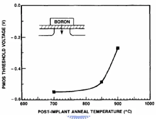
(59) Fig. 1-1 Boron penetration through the gate oxide cause the threshold voltage in BF2-impaaented p-channel devices to shift positive at anneal temperature above ~800 ℃. - 42 -.
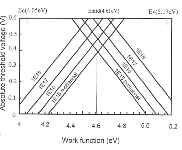
(60) Fig. 1-2 Threshold voltage versus work function of gate electrode for both nMOSFET and pMOSFET with different surface concentration.. - 43 -.
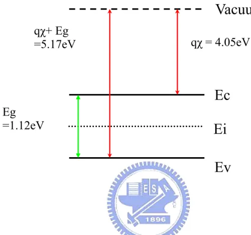
(61) Vacuum qχ+ Eg =5.17eV. qχ = 4.05eV. Ec Eg =1.12eV. Ei Ev. Fig. 1-3 Band diagram of silicon conduction and valence band.. - 44 -.
(62) Fig. 1-4 Using a single gate material for both nMOS and pMOS devices can yield symmetric but large threshold voltages. Achieving low and symmetric threshold voltages will require two different mid-gap gate materials.. - 45 -.
(63) Fig. 1-5 Schematic energy band diagram for a metal gate on a dielectric, showing extrinsic states that pin the metal Fermi level. The energy level of the extrinsic states, i.e., pinning level, could be related to the interfacial bonding defects between the metal and the dielectric. The conduction-band edge and the valence-band edge of the dielectric are denoted by Ec,d and Ev,d respectively.. - 46 -.
(64) Fig. 1-6 Cross sections illustrating the dual-metal gate process, after etching TiN/Ti and before deposition of Mo and TiN (top), and after the gate etch and source-drain implantation to show the gate stack (bottom).. - 47 -.
(65) Fig. 1-7 Schematic illustration of the process flow. (a) CMOS structure after second metal has been removed from the nMOS side. (b) CMOS structure after annealing shows that the metals on the pMOS side have interdiffused, and second metal has segregated to the dielectric interface.. - 48 -.
(66) Fig. 1-8 XPS depth profile for Ti/Ni gate electrode after the 400 ℃, 30 min interdiffusion anneal. A large concentration of Ni is present at the SiO2 interface.. - 49 -.
(67) (a). (c). (b). (d). Fig. 1-9 Fully silicide heavily implanted poly-Si gate electrode.(a)traditional poly-Si gate formation(b)B, P, As implant in poly-Si(c)metal deposition(d)silicidation by high temperature annealing.. - 50 -.
(68) (a). (f). (b). (g). (c). (h). (d). (i). (e) Fig. 1-10 The schematic of CMOS device process flow diagram. Using molybdenum silicided gate and pure molybdenum gate for nMOSFET and pMOSFET, respectively.. - 51 -.
(69) Fig. 3-1 C-V curves for pMOS capacitors with different thickness of α-silicon layer after 800 ℃ RTA.. - 52 -.
(70) Fig. 3-2 Flat-band voltage as a function of the equivalent oxide thickness. A larger flat-band voltage variation is observed between 700 ℃ and 800 ℃ RTA (work function: 4.796 eV for 700 C RTA and 4.389 eV for 800 ℃ RTA).. - 53 -.
(71) Fig. 3-3 Extracted Work function versus the RTA temperature. After 800 ℃ RTA, evidence of silicidation is observed by the change of work function.. - 54 -.
(72) Fig. 3-4 Dependence of sheet resistance of Mo/α-Si stack layers on annealing temperatures.. - 55 -.
(73) Fig. 3-5 Variation of equivalent oxide thickness of molybdenum silicide gated MOS capacitors with annealing temperature. Excellent thermal stability up to 950 ℃ can be observed.. - 56 -.
(74) Fig. 3-6 No degradation in gate leakage current is found after high-temperature annealing.. - 57 -.
(75) Fig. 3-7 Hysteresis of Mo-silicide gated MOS capacitor after 950 ℃ rapid thermal anneal still exhibits negligible.. - 58 -.
(76) Fig. 3-8 Flat-band voltage versus the equivalent oxide thickness with As-doped and undoped Mo-silicide gate (work function: 4.389 eV for undoped and 4.202 eV for As 1x1015 cm-2 dosage, 4.01 eV for As 5x1015 cm-2 dosage).. - 59 -.
(77) Fig. 3-9 The work function of Mo-silicided gate vs. As implanted dosage.. - 60 -.
(78) Fig. 3-10 Variation of equivalent oxide thickness of molybdenum silicide gated MOS capacitors with annealing temperature. Excellent thermal stability up to 950 ℃ can be observed.. - 61 -.
(79) Fig. 3-11 Flat-band voltage of pure Mo gated MOS capacitor versus the equivalent oxide thickness.. - 62 -.
(80) Fig. 3-12 Hysteresis of pure Mo gated MOS capacitor with 950 ℃ rapid thermal anneal still exhibits negligible.. - 63 -.
(81) Fig. 4-1 Extracted work function versus RTA temperature.. - 64 -.
(82) Fig. 4-2 Variation of equivalent oxide thickness of molybdenum silicide gated MOS capacitors on high-k HfO2 verse annealing temperatures. Excellent thermal stability up to 950 ℃ can be observed.. - 65 -.
(83) Fig. 4-3 The work function of Mo-silicided gate on HfO2 dielectric versus As implanted dosage after 800 ℃ RTA.. - 66 -.
(84) Fig. 4-4 Variation of equivalent oxide thickness of molybdenum silicide gated MOS capacitor with As 5x1015 cm-2 dosage on HfO2 annealing at different temperatures. Excellent thermal stability up to 950 ℃ can be observed.. - 67 -.
(85) Fig. 4-5 The C-V curve of pure Molybdenum gated MOS capacitor undergo 950 ℃ RTA.. - 68 -.
(86) Fig. 4-6 Oxide quality leakage current characteristic.. - 69 -.
(87) 簡. 姓. 名: 何 武 陵. 性. 別: 男. 歷. 出 生 日 期: 中華民國六十四年二月二日 籍. 貫: 嘉 義 縣. 地. 址: 台北縣汐止市湖前街三十三號二樓. 學. 歷: 國立台灣師範大學工業教育系 83 年 9 月 ~ 87 年 6 月 國立交通大學電子工程研究所碩士班 92 年 9 月 ~ 94 年 6 月. 碩 士 論 文: 使用完全鉬矽化之雙功函數金屬閘極技術 Dual Work Function Metal Gate Technology Using Fully Molybdenum Silicidation. - 70 -.
(88)
數據

+7

相關文件
Promote project learning, mathematical modeling, and problem-based learning to strengthen the ability to integrate and apply knowledge and skills, and make. calculated
Wang, Solving pseudomonotone variational inequalities and pseudocon- vex optimization problems using the projection neural network, IEEE Transactions on Neural Networks 17
Define instead the imaginary.. potential, magnetic field, lattice…) Dirac-BdG Hamiltonian:. with small, and matrix
Microphone and 600 ohm line conduits shall be mechanically and electrically connected to receptacle boxes and electrically grounded to the audio system ground point.. Lines in
We shall show that after finite times of switching, the premise variable of the fuzzy system will remain in the universe of discourse and stability of the adaptive control system
To investigate the characteristic of HfZrO x used a gate dielectric, we measured the gate leakage current, mobility and transistor performance.. Therefore,
The purposes of this series studies were to investigate difference between batting performance at peak level and slump level in visual cue strategy, dynamic
The core of the verification environment is the fault injection tool that can inject the transient and permanent faults into VHDL models of digital systems at chip, RTL and
