could also suppress the absorption/desorption and UV-induced migration at the back surface, causing better electrical reliability and immunity against UV radiation, respectively. All these results showed the ambient stability is greatly related to the oxygen in a-IGZO film, and the desired electrical characteristic can be achieved via the optimization of thermal annealing process.
© 2012 The Electrochemical Society. [DOI:10.1149/2.012301jss] All rights reserved.
Manuscript submitted April 18, 2012; revised manuscript received August 1, 2012. Published November 6, 2012.
Transparent amorphous conductive oxide semiconductor (TAOS) has caught lots of attention for its superior transparent characteristics and electrical performance, even in amorphous crystallization phase.1
These advantages increase the possibility of future electronic appli-cation, such as active-matrix organic light-emitting-diode displays (AMOLED), electro-phoretic display (EPD) and three dimension (3D) display technologies. Among the TAOS materials, amorphous indium (In) gallium (Ga) zinc (Zn) oxide (a-IGZO) is one of the most glaring candidates acting as semiconductor layer in thin film transistor (TFT) device.2–4 However, there are still some critical issues existed in
a-IGZO TFT, especially for the easy absorption/desorption reactions of the oxygen atom from the surrounding atmosphere.5–7 As the
oxy-gen species are absorbed in a-IGZO channel layer, they can capture electrons in the conducting channel, and then form a depletion region beneath the back channel of a-IGZO layer. By following the reaction equation of O2(g)+ e− ↔ O2(s)− , the resultant buildup of absorbed negative space charges O2−(s)easily repell conduction electrons, and positively shifts threshold voltage (Vth) of oxide TFT. Whereas the desorption of oxygen atoms in the back channel will result in the left shift of Vthvalue.8Some research groups applied passivation layers to shield the back channel of a-IGZO layer from contacting with ambient air, but sequel processes would make the impact on the characteristics of oxide semiconductor film. Therefore, the fundamental method for releasing environmental interference is to improve the a-IGZO film quality of itself.9,10In this work, the thermal annealing post-treatment
was proposed to study the effects of oxygen bonding on the char-acteristics of a-IGZO TFT device. Although the thermal annealing methods were discussed in previous reports,11,12 the device
unifor-mity and ambient stability has been little studied in relation with the role of oxygen during the thermal annealing process, especially for the channel passivation-free a-IGZO TFT. Those are critical issues for the applications of active-matrix TFT-based flat panel displays.
Experimental
The inverted staggered passivation-free a-IGZO TFT devices were fabricated on a thermal oxide capped n+ heavily-doped silicon (Si) wafer. First, the n+-type Si substrate, which also acted as the gate electrode was thermally grown a 100-nm-thick silicon-oxide (SiO2) as gate dielectric layer in a thermal furnace at 650◦C. Then, a 50-nm-thick IGZO film was subsequently deposited on it by DC sputtering system with a target of the atomic ratio of In:Ga:Zn:O= 1:1:1:4. The
zE-mail:[email protected]
pure argon (Ar) gas was only fed into the sputtering deposition system with a gas flow rate of 10 sccm under the pressure of 3× 10⁻³Torr at room temperature. Sequentially, a 50-nm-thick ITO was formed acted as source/drain electrodes and all the layers were defined by shadow mask. Finally, all samples were thermally annealed at a thermal fur-nace with N2gas flow rate of 10 L/hr at 350◦C, 400◦C, and 450◦C for one hour. X-ray photoelectron spectroscopy (XPS) was used for de-tecting the chemical components and bonding conditions of a-IGZO films. The study on environment-dependent metastability of a-IGZO TFT devices were implemented by placing samples in the atmosphere with a relative humidity of 50% at 25◦C and measured every two days, then ended in the seventh day periodically. The reliability test was conducted in a black chamber and the electrical field was given by 1 MV/cm for 180 minutes. The transfer characteristics of a-IGZO TFT under light illumination were measured in a black chamber and irradiated at the back surface of device by a halogen lamp through a band-passed filter to adjust the light wavelengths ranging from 600 nm to 300 nm. After irradiating, the light-off state was also measured to test the recovery of device. All electrical measurements were carried out with the electrical analyzer Keithley 4200.
Results and Discussion
In previous studies, the condition of 350◦C annealing process was popular for the characteristic manufacture of a-IGZO TFT device.12,13
The annealing temperature provided good device characteristics and stable reliability in the previous work. However, the effect of annealing temperatures on the ambient stability for the storage of a-IGZO TFT device has not been studied in detail. Figure1shows the evolution of transfer characteristics (ID-VG) of the 350◦C annealed a-IGZO TFT left at the atmosphere under a relative humidity of 50% at 25◦C, with time going by. As applying a 20 V gate bias, the saturation current was 4.67× 10⁻⁵A at VDS= 20 V and the on-off current ratio about 107. The mobility was 4.7 cm2/V· s extracted from the√I
D-VGScurve, and the subthreshold swing (s.s.) was 0.48 V/dec. Furthermore, the ID -VGcurve shifts toward the left after 9–day staying at the atmosphere. This indicates the passivation-free a-IGZO TFT device is unstable under the ambient. Figure2also summarizes the relationship of Vth shift between the storage duration for the channel passivation-free a-IGZO TFT left under the atmosphere. The Vthvalues were extracted from the constant drain current method, which defined the VGS at normalized drain current (NID) = 10−8 A to be the Vth value of device. It is first observed that Vth value was decreased after the thermal annealing process at 350◦C. In addition, the Vth values of a-IGZO TFT decreased apparently with the staying duration, and the
Figure 1. The transfer curves (ID-VG) of 350◦C annealing a-IGZO TFT stayed
at ambient environment with a 50% relative humidity at 25◦C for 9 days.
average value shifted from 10.2 V to 5.8 V after a 9–day staying at the atmosphere. This instability of channel passivation-free a-IGZO TFT can be attributed to the contact of a-IGZO layer with the ambient environment.14The weak bond of oxygen atoms was unstable without
enough energy for structure relaxation in annealing process, which could easily desorb out of the a-IGZO film and forming the oxygen vacancies providing free carriers.
To solve this issue, high annealing temperatures, including 400◦C and 450◦C, were adopted to treat a-IGZO TFT, and transfer character-istics of a-IGZO TFT are exhibited with different annealing tempera-tures, as shown in Fig.3. The inset reveals key electrical parameters of a-IGZO TFT device. Electrical performance of a-IGZO TFT is effectively promoted with increasing the a-IGZO annealing tempera-ture, especially at 450◦C. The enhancement of mobility and Vthcould be presumed that a-IGZO films attained more charge carriers due to the formation of thermally enhanced oxygen-vacancy after a high-temperature annealing.15Figure4also depicts the relationship of V
th shifts with the staying duration at the atmosphere. It is obvious that both the Vthvariation and the error bar are smaller in the a-IGZO TFT treated with higher annealing temperatures than that of the one with lower annealing temperature. The Vthshift value after 9-day staying is 1 V and 0.7 V for the sample annealed at 400◦C and 450◦C, re-spectively. Both of the Vthvariation and electrical uniformity were improved with the increase of annealing temperature, and the a-IGZO
Figure 2. The Vth shifts of a-IGZO TFT annealed at 350◦C stayed at the
ambient atmosphere with a 50% relative humidity at 25◦C for 9 days. Each error bar includes five different measuring results for each TFT device.
Figure 3. The comparison of ID-VGcurves of a-IGZO TFT annealed at 350◦C,
400◦C, 450◦C. The inset shows several key device parameters for the corre-sponding a-IGZO TFT.
TFT device became even stable especially after 450◦C annealing pro-cess in this work.
X-ray photoelectron spectroscopy (XPS) analysis was also con-ducted to observe the relationship between oxygen bonding and an-nealing temperatures. Figure5shows (a) In 3d, (b) Ga 2p, (c) Zn 2p and (d) O 1s spectra of a-IGZO films thermally annealed at 350◦C, 400◦C and 450◦C. The signal peaks of the In-O, Ga-O, Zn-O bonds are clearly presented in the a-IGZO film,16as shown in Figs.5a–5c.
As increasing the annealing temperature, the intensity of Zn-O peak slightly decreased, while the intensity of Ga-O peak increased. This in-dicated that relatively rich Ga-O bonds were formed than Zn-O bonds after a higher temperature annealing process. Besides, as increasing the annealing temperature, the peaks of O 1s bonding are obviously identified into two groups for the sample annealed at 350◦C (referred to as group A) and the one at above 350◦C (referred to as group B), respectively. The O 1s peak slightly shifted from 530.9 eV up to 531.4 eV, indicating the intensity of oxygen bonding in a-IGZO film was enhanced. As the annealing temperature raised up to 450◦C, the a-IGZO film maintained at a stable state, and no obvious change was observed at the O 1s peak.
Figure6aand6bshow the O 1s spectrum and curve fitting of a-IGZO film annealed at 350◦C and 450◦C, respectively. With Gaussian
Figure 4. The comparison of Vthshifts of a-IGZO TFT thermally annealed at
350◦C, 400◦C, and 450◦C for 1 hr. Each error bar includes five different mea-suring results for each TFT device. The insert shows Vthof the corresponding
Figure 5. (a) In 3d (b) Ga 2p (c) Zn 2p (d) O 1s core-level X-ray photoelectron spectrometer (XPS) spectra of a-IGZO film annealed at 350◦C, 400◦C, 450◦C annealing temperature.
Figure 6. The Gaussion curve fitting of O 1s peak in a-IGZO film annealed at (a) 350◦C and (b) 450◦C.
curve fitting, the XPS spectrum of O 1s originated from three sub-peaks, including InO species (530.3 eV), ZnO species (530.65 eV) and GaO species (531.3 eV).17–19From Figs.6aand6b, the intensity
of In-O bonding at 530.3 eV is similar for all thermally annealed a-IGZO films. However, fewer Zn-O bonding is present in the annealed a-IGZO film due to the decline in the peak intensity at 530.65 eV. On the contrary, the intensity of Ga-O bonding was enhanced after the 450◦C annealing. This result was consistent with the spectrum shown in Fig.5, which explained the right shift of O 1s peak. In a-IGZO thin film, oxygen bonding with gallium could stabilize the a-IGZO film, because of the shorter and stronger bond releasing the desorption and absorption of oxygen from environment.20,21 This result could also
well explain the better ambient stability of a-IGZO TFT after thermal annealing at higher temperatures.
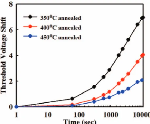
In order to ensure the proposed mechanism responsible for the ambient stability of a-IGZO TFT, a stress reliability test was conducted to accelerate the oxygen absorption/desorption at the back surface of a-IGZO active channel layer. Figure 7reveals Vth variation of a-IGZO TFT after being subjected to positive gate bias stress with an electrical field of 1 MV/cm for 180 min at the atmosphere. The variation of Vthis defined as the difference of threshold voltage before and after the application of a gate bias stress to the a-IGZO TFT device. The Vthvalue shifted toward the direction of positive voltages after positive gate bias stress (PGBS), and the variation of Vthdecreased for the a-IGZO TFT annealed at higher temperatures. Previous research documents have reported that the absorption process of oxygen species from the atmosphere can capture electrons in the a-IGZO channel layer and generate the negatively charged species (O2(s)−), as described by
Figure 7. Variation of Vthfor the thermally annealed a-IGZO TFT at 350◦C,
400◦C and 450◦C, which were applied+10 V gate bias stress (PGBS) for various durations, as measured in dark environment.
the following chemical reaction:22,23
O2(g)+ e−↔ O2(s),− [1] where e− denotes electrons, and O2 (g) and O2 (s)− representing the neutral and charged oxygen molecules, respectively, in the a-IGZO channel layer. Under positive gate bias stress, more electrons were induced in the a-IGZO channel and formed the negatively charged species (O2(s)−), which easily repelled conduction electrons in the a-IGZO TFT channel and cause the positive Vth shift. The device degradation can be released by raising the annealing temperatures to 450◦C. In the a-IGZO film, stronger chemical binding of oxygen should have good capability to reduce the oxygen absorption on a-IGZO backchannel during the positive gate bias stress. The high-temperature annealing at around 450◦C can effectively improve a-IGZO film quality and the reliability of TFT in this work.
The effect of oxygen bonding intensity on the ease of oxygen absorption/ desorption was also examined by studying the photo-sensitivity of a-IGZO TFT annealed at different temperatures. Light irradiation with wavelengths ranging from 300 nm to 600 nm was used to illuminate the a-IGZO TFT, whose optical bandgap is about 3.2 eV, and sensitive to wavelengths below 400 nm.15,24 Figure 8
shows the ID-VG curve of 350◦C annealed a-IGZO TFT device and the Vthshift of a-IGZO TFT devices annealed at different temperature is depicted in Fig.9. All samples were measured initially at the dark state, and then measured under light illumination and followed by another measurement at dark state. The threshold voltage remains a
Figure 8. The ID-VG curve of 350◦C annealed a-IGZO TFT device under
light illumination.
Figure 9. The Vthshift of a-IGZO TFT devices annealed at different
temper-atures under the light illumination and the dark state. The symbols of D-350 and D-300 indicate electrical measurements were conducted at the dark state just after turning off the light sources with 350 and 300 nm wavelengths, respectively.
slight change under visible-light illumination, while it decreases ap-parently under 350-nm UV light illumination. a-IGZO TFT devices with high annealing temperature had less Vthshifts than those with lower annealing temperature under UV light illumination. Previous research work reported that the obvious Vthshift of a-IGZO TFT un-der UV illumination can be originated from the generation of extra oxygen vacancies (Vo) after UV radiation, which may release two free electrons to form Vo+and Vo2+by light radiation around 500 nm.25,26
The results in this study showed strong oxygen binding can enhance the immunity of a-IGZO film against the UV radiation impact and the formation of Vo, thereby causing less Vthshift for the a-IGZO TFT with high annealing temperature. Besides, the electrical recovery is also rapid for the 450◦C annealed a-IGZO TFT after removing the UV illumination, due to even regular lattice architecture. The dis-torted oxygen atoms can diffuse back to the initial sites more easily after turning the light off.
Conclusions
The role of oxygen related to the ambient stability of a-IGZO TFT have been explored comprehensively in this work by the studies on device uniformity, gate bias stress and the immunity to ambient UV radiation. The passivation-free a-IGZO TFT annealed at high temperature (450◦C) performs superior electrical characteristics and the device stability. The ambient stability of a-IGZO TFT device annealed at 450◦C was good with a Vthshift of 0.7 V after 9-day stay at the atmosphere. From the XPS spectra with the Gaussian fitting, the high thermal annealing made the bonding intensity of O 1s stronger and tended to form GaOxspecies in a-IGZO film. This also showed the high-temperature annealed a-IGZO film with stronger bonding of oxygen is even stable and effectively reduce the odds of oxygen desorption to the ambient. Consequently, the film quality of a-IGZO was improved obviously, and exhibited superior resistance against gate bias stress and UV-radiation impact. This study potentially provided valuable information for the TFT-LCDs application of a-IGZO TFT device technology.
Acknowledgment
The authors thank the National Science Council of the Republic of China, Taiwan for financially supporting this research under Contract
C. H. Tu, J. J. Chang, and P. L. Chen, Applied Physics Letters, 97, 192103 (2010).
8. P. T. Liu, Y. T. Chou, and L. F. Teng, Applied Physics Letters, 95, 233504 (2010).
9. H. S. Seo, J. U. Bae, D. H. Kim, Y. Park, C. D. Kim, I. B. Kang, I. J. Chung, J. H. Choi, and J. M. Myoung,Electrochemical and Solid-State Letters, 12(9), H348 (2009). 10. W. Lim, E. A. Douglas, D. P. Norton, S. J. Pearton, F. Ren, Y. W. Heo, S. Y. Son, and
J. H. Yuh,Journal of Vacuum Science & Technology B, 28, 116 (2010).
11. H. Hosono, K. Nomura, Y. Ogo, T. Uruga, and T. Kamiya,Journal of Non-Crystalline Solids, 354, 2796 (2008).
Yeon-Gon Mo,Applied Physics Letters, 94, 112112 (2009).
22. Y. Zhang, A. Kolmakov, S. Chretien, H. Metiu, and M. Moskovits,Nano Letter, 4, 403 (2004).
23. D. Kang, H. Lim, C. Kim, I. Song, J. Park, and Y. Park,Applied Physics Letters, 90, 192101 (2007).
24. S. Y. Lee, S. J. Kim, Y. W. Lee, S. G. Park, J. Y. Kwon, and M. K. Han,ECS Trans-actions, 33(5), 313 (2010).
25. K. Takechi, M. Nakata, T. Eguchi, H. Yamaguchi, and S. Kaneko,Japanese Journal of Applied Physics, 48, 010203 (2009).