行政院國家科學委員會補助專題研究計畫
□ 成 果 報 告
▓期中進度報告
附件一
介觀及奈米尺寸結構中電子動力學及相互作用之研究(二)
Electron Dynamics and Interactions in Mesoscopic and
Nanoscale Structures (II)
計畫類別:▓ 個別型計畫 □ 整合型計畫
計畫編號:NSC 97 - 2112 - M - 009 - 017 - MY2
執行期間: 97 年 8 月 1 日至 99 年 7 月 31 日
計畫主持人: 林志忠
共同主持人:
計畫參與人員: 葉勝玄
成果報告類型(依經費核定清單規定繳交):▓精簡報告 □完整報告
本成果報告包括以下應繳交之附件:
□赴國外出差或研習心得報告一份
□赴大陸地區出差或研習心得報告一份
□出席國際學術會議心得報告及發表之論文各一份
□國際合作研究計畫國外研究報告書一份
處理方式:除產學合作研究計畫、提升產業技術及人才培育研究計畫、
列管計畫及下列情形者外,得立即公開查詢
□涉及專利或其他智慧財產權,□一年□二年後可公開查詢
執行單位:國立交通大學物理所
中 華 民 國 98 年 5 月 26 日
Two-channel Kondo effects in Al
Õ AlO
xÕ Sc planar tunnel junctions
Sheng-Shiuan Yeh1,
*
and Juhn-Jong Lin1,2,†1Institute of Physics, National Chiao Tung University, Hsinchu 30010, Taiwan 2Department of Electrophysics, National Chiao Tung University, Hsinchu 30010, Taiwan
共Received 19 December 2008; published 30 January 2009兲
We have measured the differential conductances G共V,T兲 in several Al/AlOx/Sc planar tunnel junctions between 2 and 35 K. As the temperature decreases to⬃16 K, the zero-bias conductance G共0,T兲 crosses over from a standard −ln T dependence to a novel −
冑T dependence. Correspondingly, the finite bias conductance
G共V,T兲 reveals a two-channel Kondo scaling behavior between ⬃4 and 16 K. The observed two-channel
Kondo physics is ascribed to originating from a few localized spin-21 Sc atoms situated slightly inside the AlOx/Sc interface.
DOI:10.1103/PhysRevB.79.012411 PACS number共s兲: 72.15.Qm, 64.70.Tg, 72.10.Fk, 73.40.Rw
How conduction electrons interact with local degenera-cies, which is the central theme of the Kondo effect,1 is a
long-standing issue in many-body physics. In the original Kondo effect, the local degeneracies are provided by a spin-12 impurity antiferromagnetically coupled to a single reservoir of free electrons 关the single-channel Kondo 共1CK兲 effect兴. Well below a characteristic energy, the Kondo temperature
TK, the localized moment is fully screened by the
surround-ing itinerant electrons to form a ssurround-inglet ground state, leadsurround-ing to a standard Fermi-liquid behavior.1However, Nozières and
Blandin2 proposed that, in the multichannel case, i.e., the
screening channels M⬎2S, where S is the spin of the local-ized moment, a non-Fermi-liquid behavior may occur at low temperatures. The simplest version of the multichannel Kondo phenomena is the two-channel Kondo 共2CK兲 effect 共M =2兲 which has recently attracted much theoretical3–6and
experimental7–10 attention. Apart from a physical spin, the
local degeneracies may arise from orbital quadrupolar de-grees of freedom or nearby atomic positions, i.e., two-level systems共TLS兲.3The magnetic and quadrupolar models have
been utilized to explain the specific-heat anomalies in certain heavy fermion compounds,3–5 while the TLS-induced 2CK
physics3,6has recently been experimentally realized in
nano-scale metal point contacts.7 Very lately, an artificial spin-1 2
semiconductor quantum dot coupled to two independent electron reservoirs has been elegantly constructed8to test the
2CK physics.9Besides, the 2CK effect on electrical
resistiv-ity due to TLS is argued to be found in a ThAsSe single crystal.10Thus far, there has been no observation of the 2CK
effect caused by the “simple” 3d magnetic transition-metal atoms. In this work, we report our finding of a non-Fermi-liquid behavior in Al/AlOx/Sc planar tunnel junctions where
a number of spin-12 Sc atoms are present at or slightly inside the AlOx/Sc interface.11,12
Our planar tunnel junctions are composed of three layers: an Al 共25 nm兲 film and a Sc 共60 nm兲 film separated by an insulating AlOx共1.5–2 nm兲 barrier. Both the Al and Sc films
were thermally evaporated, while the AlOxlayer was grown
on the top surface of the Al film by oxygen glow discharge.13
The low-temperature resistivities of our Al 共Sc兲 films were typically 共4 K兲⬇13 共70兲 ⍀ cm. Lock-in techniques to-gether with a bias circuitry were employed to measure the differential conductance dI/dV as a function of both bias
voltage and temperature. The modulation voltages used were smaller than kBT so that the main smearing was due to the
thermal energy. The quality of the insulating barriers was checked according to the Rowell criteria14as well as by
mea-suring the dI/dV curves below the superconducting transi-tion temperature共⬇2 K兲 of the Al films. At 0.25 K, a deep superconducting gap was evidenced in all junctions, ensuring that the conduction mechanism was governed by electron tunneling. Only the results for three representative samples 共see Table I兲 will be discussed below. However, we stress that very similar effects have been found in a dozen of junc-tions, strongly suggesting that the observed 2CK physics is robust in the Al/AlOx/Sc planar tunnel structures.
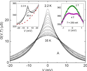
The left inset of Fig. 1shows the raw dI/dV data for the junction A at several temperatures between 2.2 and 35 K. One clearly sees conductance peaks around zero-bias voltage sitting on an asymmetric parabolic background.15After
sub-tracting this parabolic background, the excess conduc-tance ⌬G contains a dominant even contribution
Geven⬅ 1
2关⌬G共V兲+⌬G共−V兲兴 and a minor odd contribution
Godd⬅ 1
2关⌬G共V兲−⌬G共−V兲兴, where Goddⱗ0.1Geven共Ref.13兲.
In this work, we focus on the even contribution and denote it as G共V,T兲. The main panel of Fig. 1 indicates that, as T reduces, the G共V,T兲 curves become narrower and the peaks higher. Such enhanced G共V,T兲 cannot be expected from the disorder-induced suppression of electronic density of states at the Fermi level due to the electron-electron interaction effects.16
The magnitudes of the zero-bias conductance G共0,T兲 for junctions A–C are plotted in Fig. 2. At higher temperatures 共⬃16–32 K兲, G共0,T兲 obeys a −ln T law 关Fig. 2共a兲兴,
sug-TABLE I. Relevant parameters for Al/AlOx/Sc tunnel junc-tions. RJis junction resistance at 300 K, AJis junction area, T2CKis
the two-channel Kondo temperature, and Tⴱis a crossover tempera-ture defined in the text.
Sample RJ 共k⍀兲 AJ 共mm2兲 Tⴱ 共K兲 T2CK 共K兲 A 2.2 0.5⫻0.8 4 72 B 1.2 0.5⫻1.0 5 64 C 5.0 1.0⫻1.0 6 56
gesting a Kondo-type mechanism. Notably, in our intermedi-ate temperature regime of ⬃5–16 K, G共0,T兲 for all three samples obey a −
冑
T law关Fig.2共b兲兴, while a deviation fromthe −
冑
T dependence starts at about 4 K. We first notice that,in the high T regime, both the G共0,T兲⬀−ln T behavior as well as our measured finite-bias G共V,T兲 spectra13 can be
well described by a perturbative theory that considers the s-d exchange coupling between tunneling electrons and isolated localized moments which reside slightly inside the barrier.12
This observation firmly establishes the fact that localized moments are present in our oxide barriers. The formation of localized moments in our junctions most likely arose from the diffusion of some 3d1 Sc atoms slightly into the AlOx
barrier, e.g., during the fabrication process.11
It is known that in the 2CK state the conductance
g2CK共V,T兲 due to electrons tunneling through an individual
2CK impurity residing in the barrier can be expressed by
g2CK共V,T兲=g2CK共0,0兲−B
冑
T⌫共AeV/kBT兲,17–19 where A and B are nonuniversal constants which may depend on thedis-tance of the 2CK impurity from the electrode/barrier inter-face. ⌫共x兲 is a universal scaling function of x with the as-ymptotes 1 + cx2 for 兩x兩Ⰶ1, and 3
冑
兩x兩 for 兩x兩Ⰷ1, with c⬇0.0758.17,19,20 For macroscopic junctions, there may be a
number of 2CK impurities situated inside the barrier. If the interaction between these 2CK impurities can be neglected, the total conductance G2CK共V,T兲 is additive: G2CK共V,T兲
= G2CK共0,0兲−
冑
T兺iBi⌫共AieV/kBT兲, where G2CK共0,0兲=兺ig2CK共0,0兲. Therefore, the zero-bias conductance
G2CK共0,T兲 has a −
冑
T dependence. To eliminate G2CK共0,0兲,which cannot be measured directly, it is very useful to scale the conductance as a universal function of eV/kBT : 关G2CK共0,T兲−G2CK共V,T兲兴/
冑
T =兺iBi关⌫共AieV/kBT兲−1兴. This universal function leads to the asymptotes G2CK共0,T兲 − G2CK共V,T兲
冑
T =冦
b1冉
eV kBT冊
2 , 兩eV兩 kBT Ⰶ 1 b2冑
兩eV兩 kBT − b3, 兩eV兩 kBT Ⰷ 1,冧
共1兲 where b1= c兺iBiAi 2, b 2= 3兺iBi
冑
Ai, and b3=兺iBi. In the lowbias region 共兩eV兩/kBTⰆ1兲, the conductance can also be
scaled into the form
G2CK共0,T兲 − G2CK共V,T兲 = f2CK共T兲共eV/kBT兲2, 共2兲
where f2CK共T兲=b1
冑
T.The −
冑
T behavior of G共0,T兲 in Fig.2共b兲suggests that our junctions fall in the 2CK phase in this intermediate tempera-ture regime. In order to establish more and stronger evi-dences for this result, we have examined the scaling behavior of the finite bias conductance G共V,T兲. Our measured con-ductances at various temperatures are scaled according to the 2CK scaling form, Eq.共1兲, and the results are shown in Fig. 3共a兲. Notice that at intermediate temperatures 共⬃5–16 K兲, the data at different T all collapse onto a single curve for 共兩eV兩/kBT兲1/2ⱗ2.5, with the asymptotes correctly given byEq. 共1兲. That is, our scaled 关G共0,T兲−G共V,T兲兴/
冑
T⬀共eV/kBT兲2at low bias voltages of共兩eV兩/kBT兲1/2ⱗ1.4 共Ref.
21兲, while it varies linearly with 共兩eV兩/kBT兲1/2 at high bias
voltages. Therefore, the observed G共0,T兲⬀−
冑
T law togetherwith the scaling behavior of the G共V,T兲 unambiguously demonstrate that our junctions fall in a 2CK state in this intermediate temperature regime. The prefactor f2CK共T兲 in Eq.共2兲 can be extracted from the low bias data and is plotted in Fig.3共b兲. It shows that f2CK⬀
冑
T at intermediatetempera-tures, but deviates at high and low temperatures. This 2CK temperature regime for f2CK is in good accord with that found in Fig. 2共b兲for the G共0,T兲⬀−
冑
T attribute.In the high-temperature end, since the deviation of
G共0,T兲 from the −
冑
T law starts at 14T2CK共Ref.18兲, thetwo-channel Kondo temperature, T2CK, for our junctions may be
evaluated. In the low-temperature end, there is a crossover temperature, Tⴱ, below which f2CK共T兲 deviates from the −
冑
TFIG. 1. 共Color online兲 G共V,T兲 for junction A. Left inset: Raw
dI/dV data. The dotted line indicates a parabolic background
con-ductance. Right inset: Raw dI/dV data in two magnetic fields ap-plied normal to the plane of the junction.
FIG. 2. 共Color online兲 Zero-bias conductance as a function of temperature for junctions A–C.共a兲 Semilog plot of G共0,T兲 versus
T.共b兲 G共0,T兲 versus
冑T for as-prepared junctions.
共c兲 G共0,T兲ver-sus
冑T after thermal annealing.
BRIEF REPORTS PHYSICAL REVIEW B 79, 012411共2009兲
law. Our values of T2CKand Tⴱare listed in TableI. It should
be noted that, in Fig.3共a兲, deviations共red dotted lines兲 from the 2CK scaling form are seen for data with Tⱗ3.6 K.
The effect of a magnetic field H is shown in the right inset of Fig.1. We have found G共0,T兲 decreases with increasing
H and observed a Zeeman splitting of 0.45 meV at 4 T. Such
a Zeeman splitting corresponds to a g factor of 1.94, strongly indicating the presence of localized spin-12 moments, as dis-cussed above. Thus, our observed logarithmic and 2CK be-haviors of G共V,T兲 can be explained as arising from the Sc d-electron impurities. The 2CK physics in our junctions should not originate from any TLS-induced effect, since the
G共0,T兲⬀−
冑
T behavior in our junctions remained intact evenafter thermal annealing,22as is depicted in Fig.2共c兲. In
con-trast, we notice that the 2CK signals in the above-mentioned ultrasmall metal point contacts disappeared even after an-nealing at room temperatures.23On the other hand, the two-channel magnetic Kondo model developed to explain the Ce-based heavy fermion compounds should require very special
symmetries in the crystal field,3which are unlikely to happen
in our junctions. Yet, another possible candidate theory is the competition between the Kondo screening and the interim-purity interaction I proposed in the two-iminterim-purity Kondo model共2 IKM兲,24,25where the 2CK physics occurs at a
criti-cal coupling strength Ic, which separates a Kondo-screened
phase from a local-singlet phase in the ground state. How-ever, the existence of the 2CK fixed point due to the 2 IKM coupled to a single electron reservoir requires some particle-hole symmetry24,25 which is hard to conceive in our
junc-tions. Thus, the microscopic origin for our observed 2CK behavior as well as the deviation from the 2CK behavior below about 4 K is still not well understood in terms of available theories.
On the experimental side, it is intriguing that our 2CK effect is demonstrated in conventional planar tunnel junc-tions which contained 3d1transition-metal impurities. These are straightforward sample structures equipped with the sim-plest possible dynamical impurities 共S=12兲 for the Kondo phenomena.1 Moreover, it should be noted that a deviation
from the 2CK behavior has not been found in any previous experiments involving more exquisite artificial structures, such as metal point contacts7 and semiconductor quantum
dots,8where the characteristic Kondo temperatures are
rela-tively low as compared with ours. The deviation could sig-nify a crossover to a non-2CK phase as T→0 K. This issue deserves further investigations.
In summary, the 2CK non-Fermi-liquid physics has been realized in the differential conductances of Al/AlOx/Sc
pla-nar tunnel junctions. In the intermediate temperature regime,
G共0,T兲 reveals a −
冑
T dependence and G共V,T兲 obeys the2CK scaling law. At lower temperatures, a deviation in
G共0,T兲 from the −
冑
T behavior is found. These rich Kondobehaviors are believed to originate from a few localized spin-12 Sc atoms situated at or slightly inside the AlOx/Sc
interface.
The authors thank A. M. Chang, C. H. Chung, T. A. Costi, D. L. Cox, F. Guinea, T. K. Ng, J. Kroha, Z. S. Ma, G. Zarand, and A. Zawadowski for helpful discussions. This work was supported by the Taiwan National Science Council through Grant No. 96-2112-M-009-025 and by the MOE ATU Program.
1A. C. Hewson, The Kondo Problem to Heavy Fermions
共Cam-bridge University Press, Cam共Cam-bridge, 1993兲.
2P. Nozières and A. Blandin, J. Phys.共Paris兲 41, 193 共1980兲. 3D. L. Cox and A. Zawadowski, Adv. Phys. 47, 599共1998兲. 4B. Andraka, Phys. Rev. B 49, 3589共1994兲; T. S. Kim and D. L.
Cox, Phys. Rev. Lett. 75, 1622共1995兲.
5H. R. Ott, H. Rudigier, Z. Fisk, and J. L. Smith, Phys. Rev. Lett.
50, 1595共1983兲; D. L. Cox, ibid. 59, 1240 共1987兲; C. L.
Sea-man, M. B. Maple, B. W. Lee, S. Ghamaty, M. S. Torikachvili, J. S. Kang, L. Z. Liu, J. W. Allen, and D. L. Cox, ibid. 67, 2882
共1991兲.
6A. Zawadowski, Phys. Rev. Lett. 45, 211共1980兲; A. Muramatsu
and F. Guinea, ibid. 57, 2337共1986兲.
7D. C. Ralph, A. W. W. Ludwig, J. von Delft, and R. A. Buhrman,
Phys. Rev. Lett. 72, 1064共1994兲.
8R. M. Potok et al., Nature共London兲 446, 167 共2007兲; A. I. Toth,
L. Borda, J. von Delft, and G. Zarand, Phys. Rev. B 76, 155318 共2007兲.
9Y. Oreg and D. Goldhaber-Gordon, Phys. Rev. Lett. 90, 136602
共2003兲.
10T. Cichorek, A. Sanchez, P. Gegenwart, F. Weickert, A.
Woja-kowski, Z. Henkie, G. Auffermann, S. Paschen, R. Kniep, and F. FIG. 3. 共Color online兲 共a兲 2CK scaling for junctions A–C. Solid
curves stand for high T data, and dotted curves for low T data.共b兲
Steglich, Phys. Rev. Lett. 94, 236603共2005兲.
11A. F. G. Wyatt, J. Phys. C 7, 1303共1974兲.
12J. A. Appelbaum, Phys. Rev. 154, 633共1967兲; E. L. Wolf and D.
L. Losee, Phys. Rev. B 2, 3660共1970兲; This theory predicts an
approximation form G共V,T兲=A⬘− B⬘ln兵关共eV兲2
+共nkBT兲2兴/E 0
2其1/2, where A⬘and B⬘are constants, n⬇2, and E 0
is a cutoff energy.
13S. S. Yeh, Ph.D. dissertation, National Chiao Tung University,
2007.
14J. M. Rowell, in Tunneling Phenomena in Solids, edited by E.
Burnstein and S. Lundqvist共Plenum, New York, 1969兲.
15The background resulted from normal tunneling between two
metal electrodes separated by a thin barrier; W. F. Brinkman et
al., J. Appl. Phys. 41, 1915共1970兲.
16N. S. Wingreen, B. L. Altshuler, and Y. Meir, Phys. Rev. Lett.
75, 769共1995兲.
17I. Affleck and A. W. W. Ludwig, Phys. Rev. B 48, 7297共1993兲. 18M. H. Hettler, J. Kroha, and S. Hershfield, Phys. Rev. Lett. 73,
1967共1994兲.
19M. Pustilnik, L. Borda, L. I. Glazman, and J. von Delft, Phys.
Rev. B 69, 115316共2004兲.
20Y. Oreg and D. Goldhaber-Gordon, in Physics of Zero- and
One-Dimensional Nanoscopic Systems, edited by S. N. Karmakar et al.,共Springer, Berlin, 2007兲.
21Recent numerical calculations共Ref.18兲 indicate the scaled
con-ductance⬀共eV/kBT兲2even for兩eV兩⬎kBT.
22Thermal annealing of the junctions was performed in vacuum
共⬃10−5 torr兲 at 100 °C for 1 h. After annealing, the R
J共300 K兲
of samples A and B decreased to 0.83 and 0.50 k⍀, respec-tively. In plotting Fig. 2共c兲, the background conductances had been subtracted.
23D. C. Ralph and R. A. Buhrman, Phys. Rev. Lett. 69, 2118
共1992兲.
24B. A. Jones, C. M. Varma, and J. W. Wilkins, Phys. Rev. Lett.
61, 125共1988兲; J. Gan, ibid. 74, 2583 共1995兲.
25G. Zarand, C. H. Chung, P. Simon, and M. Vojta, Phys. Rev.
Lett. 97, 166802共2006兲; C. H. Chung and W. Hofstetter, Phys. Rev. B 76, 045329共2007兲.
BRIEF REPORTS PHYSICAL REVIEW B 79, 012411共2009兲