Study of the Excitation Power Dependent Internal
Quantum Efficiency in InGaN/GaN LEDs Grown on
Patterned Sapphire Substrate
Ya-Ju Lee, Ching-Hua Chiu, Chih Chun Ke, Po Chun Lin, Tien-Chang Lu, Hao-Chung Kuo, Senior Member, IEEE,
and Shing-Chung Wang
Abstract—The mechanisms of the excitation power dependent
internal quantum efficiency in InGaN/GaN multiple quantum wells (MQWs) LEDs grown on the planar and the patterned sapphire substrates (PSS) at temperature of 15 and 300 K were investigated. From observation the tendency of emission peak energy and car-rier lifetime variation in MQWs with different excitation power for both LED samples, we conclude the internal quantum effi-ciency would increase as coulomb screening effect dominates at lower carrier injection stage and decrease due to the band-filling effect at higher density stage. At room temperature, the majority of the initial injected carriers would be first consumed by the thermal activated nonradiative centers that hinder the further achievement of high-efficiency LED devices. Experimentally, the internal quan-tum efficiency of the LED grown on the PSS is∼70% and that of the LED grown on the planar sapphire substrate is∼62%. For the LED grown on the PSS, the observed higher internal quantum ef-ficiency is due to the larger activation energy Therefore, the reduc-tion of dislocareduc-tion defects and the prevenreduc-tion of injected carriers escaping from extended states would be a promising prospective for InGaN/GaN MQWs LEDs to achieve high internal quantum efficiency.
Index Terms—LEDs, GaN, Internal quantum efficiency.
I. INTRODUCTION
T
HE III-nitride material has attracted much attention due to its tremendous potential for fabricating LEDs with an emission range from UV to short visible wavelength [1], [2]. Indeed, III-nitride LEDs have been realized to a wide range of applications that include intelligent interior lighting, back-lighting unit for liquid crystal display, and general back-lighting [3]. In general, the external quantum efficiency was used to evalu-ate LED performance and was defined as the product of inter-nal quantum efficiency and light extraction efficiency. For an III-nitride LED, the internal quantum efficiency is determined primarily by growth and the associated defect formation [4].Manuscript received December 1, 2008; revised January 12, 2009. First published April 17, 2009; current version published August 5, 2009. This work was supported in part by the Taiwan National Science Council.
Y.-J. Lee is with the Institute of Electro-Optical Science and Tech-nology, National Taiwan Normal University, Taipei 116, Taiwan (e-mail: [email protected]).
C.-H. Chiu, C. C. Ke, P. C. Lin, T.-C. Lu, H.-C. Kuo and S.-C. Wang are with the Department of Photonics and the Institute of Electro-Optical Engineering, National Chiao Tung University, Hsinchu 300, Taiwan (e-mail: chchiu.eo95g@ nctu.edu.tw; [email protected]; [email protected]; timtclu@mail. nctu.edu.tw; [email protected]; [email protected]).
Color versions of one or more of the figures in this paper are available online at http://ieeexplore.ieee.org.
Digital Object Identifier 10.1109/JSTQE.2009.2014967
On the other hand, the extraction efficiency is limited by total internal reflection at the interface of GaN and air [5]. Therefore, for energy-saving reasons, an LED structure must be designed to yield either high internal quantum efficiency or high light extraction efficiency. As considering the large difference of the refractive index between GaN (n∼ 2.5) and air, most emitted light are trapped inside the LED chip and approximately only 4% of that could be extracted from a surface [6]. Thus, most reported literature to date puts attention to develop high light extraction LED structures, such as surface roughening [7], [8], photonic crystal [9], [10], chip shaping [11], backside reflec-tor [12], and so on. In contrast, the studies related to improve the internal quantum efficiency of III-nitride LEDs are rela-tively fewer. One of the reasons is the absence of a convincing approach to evaluate the internal quantum efficiency of LEDs. The general approach to evaluate the internal quantum efficiency of LEDs is to compare the photoluminescence (PL) intensity between low and room temperatures; however, the selection of pumping laser wavelength, power density, and temperature would profoundly affect the measured results. Recently, Watan-abe et al. had proposed a method to determine the internal quantum efficiency of LEDs by performing excitation power density and temperature-dependent PL [13]. In comparison to the traditional measurement method, the proposed method is believed to be more accurate since the efficiency under differ-ent pumping density was considered. Based on their results, the variation of the internal quantum efficiency of InGaN/GaN LEDs with increasing excitation power at 11 and 300 K was observed. Nevertheless, the reason for causing that variation was not clearly discovered. It is so important to understand the physical mechanisms of emission process that enables us to find out a guideline to improve the internal quantum efficiency.
In this research, we measured the internal quantum efficiency of InGaN/GaN multiple quantum wells (MQW) blue LEDs grown on c-plane planar and patterned sapphire substrates (PSS) and investigated the physical mechanism behind by analyzing the emission energy, full-width at half maximum (FWHM) of the emission spectra, and carrier recombination dynamic by time-resolved photoluminescence (TRPL) measurement.
II. EXPERIMENT
The etched patterns on sapphire substrate are 2-D hole-arrays arranged as hexagonal lattice with lattice constant of 7 µm and hole diameter of 3 µm. The etched hole is 0.5 µm in depth and has triangular-shaped C-plane in the center, surrounded 1077-260X/$25.00 © 2009 IEEE
by three {1–102} R-plane facets. The fabrication details of PSS can be found elsewhere [14], [15]. The LED structure was then grown on planar substrate and PSS by low-pressure metal-organic chemical vapor deposition.
Injected Carrier Density
= P
(hν)∗ φ ∗ dactive∗ f
∗ exp(−αG aNdG aN)
∗ [1 − exp(−αInG aNdactive)]∗ (1 − R). (1)
The LED structure consisted of a 30-nm-thick AlN nucle-ation layer, a 2-µm-thick Si-doped n-type GaN, and an unin-tentionally doped active layer with InxGa1−xN/GaN MQWs,
and a 0.2-µm-thick Mg-doped p-type GaN. The doping con-centration of n- and p-type GaN was nominally 5× 10¹⁸ and
1× 1019 cm−3, respectively. The MQW layers comprised 16
periods of an In0.15Ga0.85N well (∼2 nm) and a GaN barrier
(∼16 nm).
For excitation power and temperature-dependent PL measure-ment, the sample was mounted in a closed-cycle He cryostate and the temperature was controlled at 15 and 300 K. A frequency doubled femto-second-pulse Ti:sapphire laser of 390 nm was used to avoid the absorption of p-type GaN and directly examine the optical property of InGaN/GaN MQWs region. The lumines-cence signal dispersed through a 0.55-m monochromator was detected by the photomultiplier tube. The excitation power was changed from 5× 10⁻³ mW to 80 mW, and the corresponded injected carrier density was about 1013 to 8× 1017 cm−3. In this research, to reflect the influence of the carrier density more clearly, the incident PL power was converted to the injected car-rier density in all figures. The injected carcar-rier density is deter-mined primarily by the power of pumping laser (P ), the energy of injected photon (hv), the spot size of pumping laser (φ), the thickness of GaN and active region (dG aN, dactive), the repetition
rate of pumping laser (f ), the absorption efficiency of GaN and InGaN (αG aN, αInG aN), and the reflectance of pumping laser
(R), as expressed by the following equation [see (1), shown at the bottom of the page]. Experimentally, we choose φ = 50 µm,
dG aN = 200 nm, dactive = 270 nm, αInG aN = 105 cm−1, and
R = 0.17 to calculate the injected carrier density in our samples.
Here, we ignore the absorption of GaN, since the energy of pumping photons is less than its energy bandgap, i.e., αG aN = 0.
For the measurement of temperature dependent TRPL, the fre-quency doubled femto-second-pulse Ti:sapphire laser was op-erated on 390 nm with 2 mW. The repetition rate of the laser is 76 MHz whose time interval is 13 ns. The luminescence de-cay was measured with time correlated single photon counting system in conjunction with a 0.55-m monochromator. Time res-olution for the detection is about 4 ps. The setup details of temperature dependent PL and TRPL are shown in Fig. 1.
III. RESULTS ANDDISCUSSION
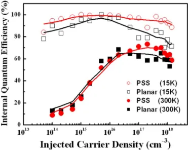
Fig. 2 shows the measured power-dependent efficiency as a function of injected carrier density at 15 and 300 K for both LEDs grown on the planar sapphire substrate and PSS. The effi-ciency is defined as the collected photon number divided by the
Fig. 1. Setup of temperature-dependent PL and TRPL to evaluate the internal quantum efficiency of LED samples.
Fig. 2. Internal quantum efficiency as function of injected carrier density at 15 and 300 K for the LEDs grown on the planar sapphire substrate and the PSS.
injected photon numbers and all normalized to the maximum ef-ficiency [13]. For the LED grown on planar sapphire substrate, one could clearly see that the internal quantum efficiency in-creases with injected carrier density to reach its maximum and decreases as the injected carrier density further increases. The tendency of two efficiency curves at 15 and 300 K is quite sim-ilar. But under low-injection carrier density range, the internal quantum efficiency at 300 K increases more pronounced than it at 15 K. Moreover, the corresponding density to the peak effi-ciency (∼62%) in 300 K is at injected carrier density of about 1017 cm−3, which is lager than it at 15 K, about 1016 cm−3. A much larger variation of the internal quantum efficiency was observed over the injection carrier range at 300 K than 15 K.
For the LED grown on the PSS, a similar dependence of the internal quantum efficiency on the injected carrier density was observed. However, in term of the peak efficiency (∼70%) in 300 K at injected carrier density of 1× 1017cm−3, the internal
quantum efficiency of LED grown on the PSS was enhanced by
∼13%. It means that under the same injected power of
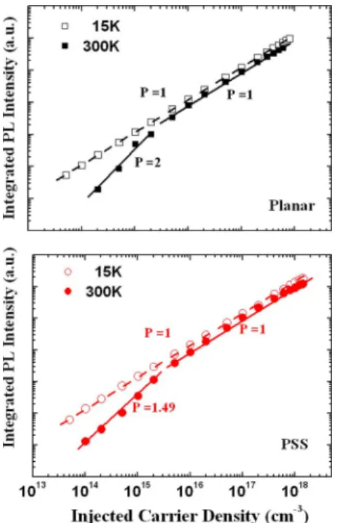
Fig. 3. Integrated PL intensity as function of injected carrier density at 15 and 300 K for both LEDs grown on the planar sapphire substrate (top) and the PSS (bottom).
photon carriers within the active region, as compared to the conventional LED structure grown on planar sapphire substrate. We believe the higher internal quantum efficiency for the LED grown on the PSS is due to the better crystalline quality, at-tributed to the interaction between stack faults and threading dislocations, as studied in our previous work [15]. We now dis-cuss the mechanism responsible for the dependence of internal quantum efficiency on the injected carrier density for both LEDs grown on planar sapphire substrate and PSS.
In general, the collected PL intensity, L, is proportional to the injected carrier density, I, with a power index P which could be expressed as [16], [17]
LαIP (2) where parameter P physically reflects the various recombination processes. If P equals 1, it indicates the radiative recombination dominates. On the other hand, if P > 1, the Shockley–Read– Hall recombination occurs, relating to the presence of nonra-diative centers that provide a shunt path to the current. Fig. 3 summarized the relationship between injected carrier density and the PL intensity for both LED grown on planar sapphire substrate (top of Fig. 3) and PSS (bottom of Fig. 3).
At 15 K for both samples, the intensity is linearly varied with excitation power density (P = 1), which indicates that the radiative recombination dominates the recombination process at all injected carrier density range and the nonradietive centers are quenched at low temperature. However, under low excitation power density at 300 K, the superlinear dependence of L on I is observed for both samples, showing that the defect related non-radiative recombination dominates in this low carrier injection range. But as injected carriers continuously increased, the linear
dependence of the PL intensity to the injected carrier density is exhibited. It must be noted here for both samples in 300 K, the value of P decreases to 1 gradually with the increasing of injected carrier density, instead of jumping from 1.49 to 1 for PSS sample (or 2 to 1 for planar sample). It means the nonra-diative centers are saturated and lead to the gradual suppression of the nonradiative recombination with the injected carrier den-sity; therefore, the radiative recombination starts to dominate the recombination process, resulting in the pronounced increas-ing of the internal quantum efficiency, as shown in Fig. 2, for the region of injected carrier density less than 1017 cm−3. In
addition, since the LED grown on the planar sapphire substrate has higher threading dislocations than that grown on the PSS, the value of P in the superlinear zone is greater for the LED grown on planar sapphire substrate (P = 2) than for the LED grown on PSS (P = 1.49).
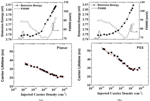
To further study the mechanisms responsible for the varia-tion of the internal quantum efficiency in Fig. 2, more optical properties were investigated as below. Fig. 4 shows the emis-sion peak energy and the FWHM of spectra as a function of the injected carrier density at 15 K for both LEDs grown on the planar sapphire substrate [Fig. 4(a)] and the PSS [Fig. 4(b)]. The corresponding carrier lifetime for both samples was also measured and provided in Fig. 4 to support the analysis of car-rier dynamics. In Fig. 4(a), for the LED grown on the planar sapphire substrate in 15 K, several unique optical properties were observed. First, the emission peak energy gradually in-creases with the injected carrier density. Second, the FWHM of spectra shrinks when the injection carrier density ranging from 5× 1013 cm−3 to 1× 1016 cm−3, and an opposite trend
was observed as the injection carriers further increased. In gen-eral, there are two possible mechanisms for the blueshift of emission energy with increasing injected carrier density. The first is coulomb screening of the quantum-confined Stark effect (QCSE). The increasing of injected carrier density weakens the QCSE, and that results in the increasing of transition energy. As the screening effect dominates the emission process, it accom-panied a reduction in FWHM. The second is band-filling effect of localized states.
Due to indium composition inhomogeneity and monolayer thickness fluctuation of the InGaN MQWs, self-organized In-rich region is generated in InGaN active region, resulting in potential fluctuation of the energy bandgap [18]–[20]. Fur-ther increasing of injected carrier density, the filling effect of high-energetic localized centers starts interfering and becomes dominated; that also induces a blueshift of emission energy. However, unlike the effect of QCSE, this effect accompanies the broadening of FWHM. Clearly, we can conclude that in the region of injected carrier density from∼5 × 1013 cm−3 to
∼1 × 1016 cm−3, the gradual increase of emission energy and shrink of FWHM for the LED grown on planar sapphire sub-strate is mainly due to the coulomb screening of the QCSE, and that increases the overlap probability of wavefunction of electron and hole. Therefore, in the same region of injected carrier density (∼5 × 1013 cm−3 to∼1 × 1016 cm−3), its
in-ternal quantum efficiency also gradually increases, as shown in Fig. 2 (open square). As the injected carrier density is further
Fig. 4. Emission energy, FWHM and carrier lifetime as a function of injected carrier density at 15 K for the LED grown on (a) the planar sapphire substrate and (b) the PSS.
increased (> 1× 1016 cm−3), band filling of localized states
starts interfering and becomes dominated; the effect prompts the injected carriers to escape more easily from localized states. As a result, the internal quantum efficiency was further deteriorated with the injected carrier density larger than 1× 1016cm−3.
In the bottom of Fig. 4(a), we observed the gradually reduced carrier lifetime with the increasing of the injected carrier den-sity. The decreasing of carrier lifetime with increasing injected carrier density could be attributed to the coulomb screening of internal electric in InGaN MQWs [21]. As injected carrier density in the quantum well (QW) increases, more excited car-riers can screen the built-in electric field in QW and that ani-mates the recombination of electron-hole pair. As a result, the carrier recombination rate was accelerated, leading to a decre-ment of carrier lifetime. For higher injection carrier density (> 1× 1016 cm−3), we observe that the carrier lifetime keeps
decreasing, but a saturated tendency as injected carrier density higher than 2× 1017cm−3. That is mainly because the carrier at
higher state by band-filling effect would have shorter lifetime. And as long as these higher energy states were fully occupied, the corresponding carrier lifetime of emitted photon will keep constant, even with further injection of carrier density. Here, it is clear that our measurement of carrier lifetime well agrees with the shift of main emission peak.
As for the LED grown on the PSS in 15 K [Fig. 4(b)], ba-sically we can adopt the same carrier dynamics to clarify the dependence of emission peak energy and the FWHM on the injected carrier density. However, in the bottom of Fig. 4(b), we observe that under exactly the same injected carrier density, the carrier lifetime of the LED grown on the PSS is around 10 ns longer than that of the LED grown on the planar sapphire sub-strate. We believe it is due to the fewer threading dislocations in the LED grown on the PSS. In general, the nonradiative recom-bination rate is much quicker than the radiative recomrecom-bination
rate, and more nonradiative centers were expected in the LED grown on the planar sapphire substrate. Therefore, in term of the carrier lifetime of emitted photon, the LED grown on the PSS will have longer carrier lifetime than that grown on the planar sapphire substrate. It is also consistent with the evaluation of the internal quantum efficiency in Fig. 2, as one can observe the higher efficiency value on the LED grown on the PSS than that grown on the planar sapphire substrate in 15 K.
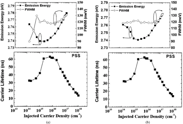
To further examine the mechanism responsible for the ten-dency of the internal quantum efficiency in 300 K, we perform the similar analysis for both LED devices. For the LED grown on the planar sapphire substrate as shown in Fig. 5(a), we could divide three parts of this curve for discussion. At the first glance, the tendency in the region of the injected carrier density from
∼5 × 1015 cm−3 to∼7 × 1017 cm−3 in Fig. 5(a), is very simi-lar to that at 15 K. Moreover, as compared to the top of Fig. 3 (solid square, 300 K), the parameter P in this region equals 1, indicating the radiative recombination dominates. Therefore, the physical mechanisms of this region can be classified to two stages: 1) the preliminary dominated coulomb screening of the QCSE and 2) the subsequent interfering of band filling effect of localized states.
However, for the initial case of the region with the injected carrier density from 1× 1014cm−3to 1× 1015cm−3, different
phenomena were observed. First, in contrast to the results mea-sured at 15 K as shown in Fig. 4(a), the emission energy shows the redshift and the FWHM broadens with increasing injected carrier density. Second, the parameter P in this region equals 2, indicating the nonradiative recombination dominates the car-rier recombination process. Third, as compared to Fig. 4(a), it can be found the emission energy at 300 K under low injected carrier density is higher than that at 15 K, which shows that the carriers recombined at higher energy states at 300 K under low injected carrier density condition. Finally, in the bottom
Fig. 5. Emission energy, FWHM and carrier lifetime as a function of injected carrier density at 300 K for the LED grown on (a) the planar sapphire substrate and (b) the PSS.
of Fig. 5(a), the carrier lifetime increases to the maximum of
∼45 ns with the injected carrier density from 1 × 1014cm−3 to
1× 1015cm−3 and remains unchanged from 1× 1015cm−3 to 5× 1015cm−3. As further increase the injected carrier density (> 5× 1015 cm−3), the corresponding carrier lifetime droops gradually.
To summarize the different phenomena mentioned above, at lowest injected carrier density, due to nonradiative process dom-inates the carrier recombination process (P = 2), the carrier lifetime is shortened and that prompts excited carriers to re-combine at higher energy extended states before reaching into lower energy localized states [22]. Thus as compared to the recombination in low-energy localized state in 15 K, the tran-sition of these higher energy extended states would emit higher photon energy. Since there may exist many of higher energy ex-tended states, this kind of recombination would accompany by the broadening of FWHM. Moreover, with the increasing of the injected carrier density from 1× 1014cm−3to 1× 1015 cm−3, the nonradiative recombination was gradually bleached out and, on the contrary, the radiative process comes to be dominating. Hence, an increment of lifetime was observed in this region [bot-tom of Fig. 5(a)]. Once the carrier lifetime increases, the excited carriers can transfer from higher extended states to lower local-ized states and get accompanied with the redshift of emission energy. As a result, in the region of injected carrier density from 1× 1014 cm−3 to 1× 1015 cm−3 in 300 K, we can
ex-pect the higher emission energy than that in 15 K, the redshift of emission energy, the broadening of the FWHM, and the in-creasing of the carrier lifetime. For the region of the injected carrier density from 1× 1015cm−3to 5× 1015cm−3, it could
be seemed as a quasi-equilibrium state of the injected carriers, thus an unchanged of carrier lifetime was observed. After that (> 5× 1015 cm−3), similar phenomenon as we discussed in Fig. 4(a) was observed. Therefore, we could conclude that for the LED grown on the planar sapphire substrate, the main mech-anism for causing the difference between the internal quantum efficiency curves in 15 and 300 K is the thermal activated non-radiative centers especially at the stage of low injected carrier density. The majority of injected carrier was exhausted by the nonradiative centers and fails to effectively screen the QCSE, resulting in low internal quantum efficiency at 300 K.
In Fig. 5(b), we show the emission energy and the FWHM as function of injected power density at 300 K for the LED grown on the PSS. The corresponding carrier lifetime for the sample is also shown in the bottom of Fig. 5(b). As compared to the sam-ple LED measured in 15 K [Fig. 4(b)], for the injected carrier density from 1× 1014 cm−3to 1× 1015cm−3, we can observe
the higher emission energy, the redshift of emission energy, and the increasing of the carrier lifetime, and that is similar to the previous analysis for the LED grown on the planar sapphire substrate. However, we do not observe the broadening of the FWHM in this region. We believe it is due to the fewer thread-ing dislocations existthread-ing in the LED grown the PSS, and thus reduces the transition from higher energy extended states. For the inject carrier density from 1× 1015cm−3to 5× 1015cm−3,
we also observe the unchanged of the carrier lifetime; however, its maximum carrier lifetime of∼60 ns is longer than that of the LED grown on the planar sapphire substrate (∼45 ns). It means fewer nonradiative centers would interfere and affect the transition of injected carriers, and that is well consistent with
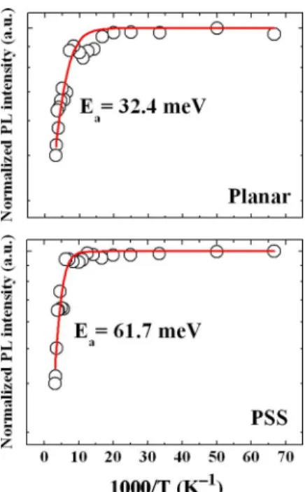
Fig. 6. Normalized integrated PL intensity as a function of 1/T for LEDs grown on the planar sapphire substrate (top) and the PSS (bottom). The activation energy is obtained from the Arrhenius plot.
the experimental observation of FWHM. Again, for the injected carrier density larger than 5× 1015 cm−3, the radiative recom-bination becomes dominated (P = 1) and that would lead to the preliminary coulomb screening of the QCSE and the subsequent band filling effect of localized states as we mentioned before.
Finally, we would like comment briefly on the origin of higher internal quantum efficiency for the LED grown on the PSS. Fig. 6 shows the Arrhenius plot of the normalized integrated PL inten-sity for both LED grown on the planar sapphire substrate (top of Fig. 6) and the PSS (bottom of Fig. 6) over the temperature range from 15 to 300 K.
The fit activation energy for the LED grown on the planar sapphire substrate and the PSS are 32.4 meV and 61.7 meV, respectively. In general, the activation energy can be explained by the ability to confine the carriers within the potential min-ima. Thus, the higher value of the activation energy indicates the stronger confinement of injected carriers and that certainly promises the higher internal quantum efficiency.
IV. SUMMARY
In summary, the physical mechanisms affecting the internal quantum efficiency in InGaN/GaN MQWs LEDs grown on the planar sapphire substrate and the PSS under 15 and 300 K have been studied. At room temperature, the majority of the ini-tial injected carrier was used to suppress the thermal activated nonradiative centers. As the injected carrier density increased, the internal quantum efficiency was improved at the region of screening effect dominated and decreased when band-filling ef-fect dominated. By the comparison of optical properties for both LED samples, to achieve a high internal quantum effi-ciency GaN-based LED, it would be beneficial to decrease the defect density, weaken the internal electric field in the QW, and
increase the depth of localized states to hinder carriers escaping to extended states. This result would provide a useful guidance to fabricate a high-performance LED with high internal quantum efficiency.
ACKNOWLEDGMENT
The authors would like to thank Dr. T. C. Hsu of Epistar Co. Ltd. in Taiwan for useful discussion. The work was supported by the MOE ATU program and in part by the National Science Council in Taiwan under contract numbers of NSC 95-2120-M-009-008, NSC 95-2752-E-009-007-PAE, and NSC 95-2221-E-009-282.
REFERENCES
[1] S. Nakamura, S. Pearton, and G. Fasol, The Blue Laser Diode: The
Com-plete Story, 2nd ed. Berlin, Germany: Springer-Verlag, 2000. [2] E. F. Schubert, Light-Emitting Diodes, 2nd ed. Cambridge, U.K.:
Cam-bridge Univ. Press, 2006.
[3] R. D. Dupuis and M. R. Krames, “History, development, and applica-tions of high-brightness visible light-emitting diodes,” IEEE J. Lightw.
Technol., vol. 26, no. 9, pp. 1154–1171, May 2008.
[4] S. Nakamura, “The roles of structural imperfections in InGaN-based blue light-emitting diodes and laser diodes,” Science, vol. 14, pp. 956–961, 1998.
[5] M. Broditsky and E. Yablonovitch, “Light-emitting diode extraction effi-ciency,” in Proc. SPIE, 1997, vol. 3002, pp. 119–122.
[6] A. Billeb, W. Grieshaber, D. Stocker, E. F. Schubert, and R. F. Karlicek Jr., “Microcavity effects in GaN epitaxial films and in Ag/GaN/sapphire structures,” Appl. Phys. Lett., vol. 70, pp. 2790–2792, 1997.
[7] Y. J. Lee, H. C. Kuo, S. C. Wang, T. C. Hsu, M. H. Hsieh, M. J. Jou, and B. J. Lee, “Increasing the extraction efficiency of AlGaInP LEDs via n-side surface roughening,” IEEE Photon. Technol. Lett., vol. 17, no. 11, pp. 2289–2291, Nov. 2005.
[8] T. Fujii, Y. Gao, R. Sharma, E. L. Hu, S. P. DenBaars, and S. Nakamura, “Increase in the extraction efficiency of GaN-based light-emitting diodes via surface roughening,” Appl. Phys. Lett., vol. 84, pp. 855–857, 2004. [9] S. Fan, P. R. Villeneuve, J. D. Joannopoulos, and E. F. Schubert, “High
extraction efficiency of spontaneous emission from slabs of photonic crys-tals,” Phys. Rev. Lett., vol. 78, pp. 3294–3297, 1997.
[10] T. N. Oder, K. H. Kim, J. Y. Lin, and H. X. Jiang, “III-nitride blue and ultraviolet photonic crystal light emitting diodes,” Appl. Phys. Lett., vol. 84, pp. 466–468, 2004.
[11] C. C. Kao, H. C. Kuo, H. W. Huang, J. T. Chu, Y. C. Peng, Y. L. Hsieh, C. Y. Luo, S. C. Wang, C. C. Yu, and C. F. Lin, “Light-output enhance-ment in a nitride-based light-emitting diode with 22 degrees undercut sidewalls,” IEEE Photon. Technol. Lett., vol. 17, no. 2, pp. 19–21, Jan. 2005.
[12] Y. J. Lee, J. M. Hwang, T. C. Hsu, M. H. Hsieh, M. J. Jou, B. J. Lee, T. C. Lu, H. C. Kuo, and S. C. Wang, “GaN-based LEDs with Al-deposited V-shape sapphire facet mirror,” IEEE Photon. Technol. Lett., vol. 18, no. 5, pp. 724–726, Mar. 2006.
[13] S. Watanabe, N. Yamada, M. Nagashima, Y. Ueki, C. Sasaki, Y. Ya-mada, T. Taguchi, K. Tadatomo, H. Okagawa, and H. Kudo, “Internal quantum efficiency of highly-efficient InxGa1−xN-based near-ultraviolet light-emitting diodes,” Appl. Phys. Lett., vol. 83, pp. 4906–4908, 2003. [14] Y. J. Lee, J. M. Hwang, T. C. Hsu, M. H. Hsieh, M. J. Jou, B. J. Lee,
T. C. Lu, H. C. Kuo, and S. C. Wang, “Enhancing output power of GaN-based LEDs grown on chemical wet etching patterned sapphire substrate,”
IEEE Photon. Technol. Lett., vol. 18, no. 10, pp. 1152–1154, May 2006.
[15] Y.-J. Lee, T. C. Lu, H. C. Kuo, S. C. Wang, K. W. Ng, K. M. Lau, Z.-P. Yang, A. S. P. Chang, and S.-Y. Lin, “Study of GaN-based light emitting diodes grown on chemical wet etching-patterned sapphire sub-strate with V-shaped pits roughening surfaces,” IEEE J. Lightw. Technol., vol. 26, no. 11, pp. 1455–1463, Jun. 2008.
[16] I. Ma’rtil, E. Redondo, and A. Ojeda, “Influence of defects on the electrical and optical characteristics of blue light-emitting diodes based on III–V nitrides,” J. Appl. Phys., vol. 81, pp. 2442–2444, 1997.
[17] X. A. Cao, E. B. Stokes, P. M. Sandvik, S. F. LeBoeuf, J. Kretchmer, and D. Walker, “Diffusion and tunneling currents in GaN/InGaN multiple
quantum well light-emitting diodes,” IEEE Electron Device Lett., vol. 23, no. 9, pp. 535–537, Sep. 2002.
[18] S. Chichibu, T. Sota, K. Wada, and S. Nakamura, “Exciton localization in InGaN quantum well devices,” J. Vac. Sci. Technol. B, vol. 16, pp. 2204– 2214, 1998.
[19] T. Wang, D. Nakagawa, J. Wang, T. Sugahara, and S. Sakai, “Photolumi-nescence investigation of InGaN/GaN single quantum well and multiple quantum wells,” Appl. Phys. Lett., vol. 73, pp. 3571–3573, 2007. [20] T. Kuroda and A. Tackeuchi, “Influence of free carrier screening on the
luminescence energy shift and carrier lifetime of InGaN quantum wells,”
J. Appl. Phys., vol. 92, pp. 3071–3074, 2002.
[21] Y. Narukawa, S. Saijou, Y. Kawakami, S. Fujita, T. Mukai, and S. Naka-mura, “Radiative and nonradiative recombination processes in ultraviolet light-emitting diode composed of an In0 . 0 2Ga0 . 9 8N active layer,” Appl. Phys. Lett., vol. 74, pp. 558–560, 1999.
[22] Y. H. Cho, G. H. Gainer, A. J. Fischer, J. J. Song, S. Keller, U. K. Mishra, and S. P. DenBaars, ““S-shaped” temperature-dependent emission shift and carrier dynamics in InGaN/GaN multiple quantum wells,” Appl.
Phys. Lett., vol. 73, pp. 1370–1372, 1998.
Ya-Ju Lee received the B.S. degree in physics from
the National Central University, Jhongli, Taiwan, in 2000 and the M.S. and Ph.D. degrees from the Depart-ment of Photonics, National Chiao Tung University, Hsinchu, Taiwan, in 2002 and 2007, respectively.
In 2008, he was a Postdoctoral Research Asso-ciate in Future Chips Constellation and Department of Physics, Applied Physics and Astronomy, Rensse-laer Polytechnic Institute, Troy, NY. Since February 2009, he has been a Faculty Member of the Institute of Electro-Optical Science and Technology, National Taiwan Normal University, Taipei, Taiwan.
Ching-Hua Chiu received the B.S. and M.S. degrees
in power mechanical engineering from the National Tsing Hua University, Hsinchu, Taiwan, in 2004 and 2006, respectively. He is currently working toward the Ph.D. degree in the Department of Photonics, Na-tional Chiao Tung University, Hsinchu.
His current research interests include the verti-cal LED and high-performance GaN-based LED via nanotechnology.
Chih Chun Ke is currently a Graduate Student in
the Institute of Electro-Optical Engineering, National Chiao Tung University, Hsinchu, Taiwan.
His current research interest includes the optical measurement and characterization of efficiency droop on GaN-based LEDs.
Po Chun Lin received the B.S. degree from the Institute of Electro-Optical
Engineering, National Chiao Tung University, Hsinchu, Taiwan, in 2008. His current research interest includes the internal quantum efficiency on blue LED and material optical properties measurement.
Tien-Chang Lu received the B.S. degree in
electri-cal engineering from the National Taiwan University, Taipei, Taiwan, in 1995, the M.S. degree in electri-cal engineering from the University of Southern Los Angeles, Los Angeles, CA, in 1998, and the Ph.D. de-gree in electrical engineering and computer science from the National Chiao Tung University, Hsinchu, Taiwan, in 2004.
From August 2005, he has been a Faculty Member at the Department of Photonics, National Chiao Tung University.
Hao-Chung Kuo (M’99–SM’06) received the B.S.
degree in physics from the National Taiwan Uni-versity, Taipei, Taiwan, the M.S. degree in electri-cal and computer engineering from Rutgers Univer-sity, New Brunswick, NJ, in 1995, and the Ph.D. de-gree from the Electrical and Computer Engineering Department, University of Illinois at Urbana Cham-paign, Urbana, in 1999.
From 1993 to 1995, he was a Research Consultant in Lucent Technologies, Bell Laboratories, and from 1999 to 2001 he was a Member of Technical Staff in Fiber-Optics Division at Agilent Technologies. From 2001 to 2002, he was with LuxNet Corporation. Since October 2002, he has been a Faculty Member of the Institute of Electro-Optical Engineering, National Chiao Tung University, Hsinchu, Taiwan, where he is now the Associate Dean, Office of International Affairs. His current research interests include semiconductor lasers, vertical-cavity surface-emitting lasers, blue and UV LED lasers, quantum-confined op-toelectronic structures, opop-toelectronic materials, and solar cell. He has authored or coauthored more than 140 journal papers and holds 6 granted and 10 pending patents.
Prof. Kuo is an Associate Editor of IEEE/OSA JOURNAL OFLIGHTWAVE
TECHNOLOGYand JSTQE-special issue Solid State Lighting. He received the Ta-You Wu Young Scholar Award from the National Science Council and the Young Photonics Researcher Award in 2007.
Shing-Chung Wang received the B.S. degree from
the National Taiwan University, Taipei, Taiwan, the M.S. degree from the National Tohoku University, Sendai, Japan, and the Ph.D. degree from Stanford University, Stanford, CA, in 1971, all in electrical engineering.
From 1965 to 1967, he was a Faculty Member at the National Chiao Tung University, and from 1971 to 1974 he was a Research Associate at Stanford University. From 1974 to 1985, he was a Senior Re-search Scientist at Xerox Corporation, and from 1985 to 1995 he was a Consulting Scientist at Lockheed-Martin Palo Alto Research Laboratories. In 1995, he joined the Institute of Electro-Optical Engineering, National Chiao Tung University, Hsinchu, Taiwan, as a Faculty Member. His current research interests include semiconductor lasers, vertical-cavity surface-emitting lasers, blue and UV lasers, quantum-confined optoelectronic structures, optoelectronic materials, diode-pumped lasers, and semiconductor laser appli-cations.
Prof. Wang is a Fellow of the Optical Society of America and a recipient of the Outstanding Scholar Award from the Foundation for the Advancement of Outstanding Scholarship.