國 立 交 通 大 學
電信工程學系
博 士 論 文
以等效電路法設計之縮小化及去耦合化
印刷天線
Miniaturization and Decoupling Design of
Printed Antennas by the
Equivalent Circuit Approach
研 究 生:王侑信
Yu-Hsin Wang
指導教授:鍾世忠 博士
Dr. Shyh-Jong Chung
以等效電路法設計之縮小化及去耦合化印刷
天線
Miniaturization and Decoupling Design of
Printed Antennas by
the Equivalent Circuit Approach
研究生:王侑信
Student:
Yu-Hsin
Wang
指導教授:鍾世忠 博士
Advisor: Dr. Shyh-Jong Chung
國立交通大學
電信工程學系
博士論文
A Dissertation
Submitted to Department of Communication
Engineering
College of Electrical and Computer Engineering
National Chiao Tung University
in Partial Fulfillment
of the Requirements
for the Degree of Doctor of Philosophy
in
Communication Engineering
Hsinchu, Taiwan
摘要
摘要
摘要
摘要
本論文旨在研究縮小化天線與多天線去耦合的設計。基於現代無線通訊產品 尺寸日益縮小的趨勢,以及經常整合多種無線系統於其中,縮小化天線以及去耦 合設計為兩大重要議題。本研究中所有的設計皆使用等效電路模型來解釋天線輸 入阻抗的特性。內容主要在於小型天線的設計上提出了新的設計方式,採用電路 合成的方式來合成天線,同時可達到共振頻率與阻抗匹配。而去耦合化的設計則 提出兩種方式,包含了在電路端提高隔離度的方式,以及使用扼流器阻擋耦合電 流的方式,兩者面積皆小於文獻中同類型設計。基於以縮小化為前提,本論文中 所提出的架構皆適用於可攜性的無線通訊產品。 本研究將天線分成兩大類,第一類為利用足夠的長度產生波傳導自然共振的 設計,例如:縮小化的四分之一波長倒 F 天線。第二類則是使用電路合成產生共 振的設計,此為本論文所提出的重點。針對此兩種天線,本論文皆提出縮小化的 設計。首先,本論文提出利用螺旋繞線的方式縮小傳統倒 F 天線,同時達到雙頻 的效果,以及利用高介電系數的陶瓷材料縮小四股螺旋天線的方式。兩者分別為 四分之一波長與一個波長的共振形式,各達到原始面積的 50%及體積的 2.7%的 縮小化效果,並且都有等效電路分析其操作模式。另一方面,以電路合成的設計 方式,提出了利用串連等長左右手傳輸線的概念來設計開路共振腔,並更進一步 的利用短槽孔作為輻射單元,並採用兩顆總集電容,設計出小型天線且實現頻率 可調整的功能,僅需要 9 mm x 1.5 mm 的槽孔尺寸即可操作在 1.35 GHz 至 2.45 GHz。此兩種設計都是從等效電路出發,再利用印刷元件來完成佈局實現天線功 能,所提出的等效電路可解釋共振頻率以及阻抗匹配的機制。關於去耦合的設 計,針對小尺寸的需求開發了縮小化的去耦合架構,使用地緣扼流器。地緣扼流 器是使用印刷電路單元實現,其可等效為一個並聯諧振器,能阻擋流經地面邊緣 的電流,利用此一特性可以幫助增加兩隻天線的隔離度。此一設計具有小型化以 及高適應性的優點,且理論與實作皆已完備並可相互驗證。Abstract
This dissertation presents the miniaturized antennas and decoupling structures, which are two important issues in mobile wireless applications. All the proposed designs are developed by the equivalent circuit approach in order to understand the impedance features more clearly. The new design concept for antenna has been presented, which is to construct antennas through circuit synthesis. Methods of decoupling are also revealed, including blocking and canceling mechanism. All the proposed structures are compact and low cost that meets the requirement of portable devices nowadays.
The presented miniaturized antennas are divided into two catalogs, the wave resonance type and circuit synthesis type. In natural resonance type, the printed dual-band inverted-F is miniaturized by spiraling the tail of the open-end strip that can simultaneously achieve dual-band operation and size reduction (50%). The dielectric loaded quaduature helix antenna using ceramic rod (relative permittivity = 40) dramatically reduces the volume to be 2.7% of air-loaded one. Both are analyzed by equivalent circuits. The designs of circuit approach utilize the short slot radiator as an inductive element to synthesize the equivalent circuit for antennas. A cascaded right/left-handed transmission line, with opposite phase delay, as a feed is used to create the resonance at operation frequency. An improved design of using two capacitors on a short slot radiator further shrinks the antenna size (9 mm by 1.5 mm for 2.4GHz) and gains more design flexibility. By using varactors it can become a frequency tunable antenna (9 mm by 1.5 mm for 1.35-2.45GHz, measured).
Decoupling technology shows importance in integrated multiple systems and Multiple-Input-Multiple-Output (MIMO) system. For the small device, the decoupling design should also be compact. There is a decoupling method proposed. The current choke composed of printed elements with the function of blocking the induced current on the ground edge. The design is compact and easily integrated in most devices.
誌謝
誌謝
誌謝
誌謝
首先感謝指導教授多年來的栽培提攜和口試委員的建議與評論。還要感謝實 驗室眾多的學長姐和學弟妹,因為有你們,論文才能如此順利地完成。 謝謝大家(鞠躬)。Content
摘要...i Abstract ...ii 誌謝... iii Content...iv List of Tables...viList of Figures ...vii
Chapter 1 Introduction ...1
1.1 Background and Motivation ...1
1.2 Literature Survey ...3
1.2.1 Miniaturized Antennas ...3
1.2.2 Decoupling Methods...9
1.2.3 Antenna Equivalent Circuit Analysis ...13
1.3 Antenna synthesis by the Equivalent Circuit Approach...15
1.4 Contributions...16
Chapter 2 Miniaturized Antennas with Wave Resonances ...18
2.1 Spiraled Printed Inverted-F Antenna ...18
2.1.1 Antenna Configuration...18
2.1.2 Equivalent Circuit Analysis ...19
2.1.3 Experimental Results ...23
2.1.4 Summary ...26
2.2 Dielectric-loaded Quaduature Helix Antenna ...27
2.2.1 Antenna Configuration...28
2.2.2 Equivalent Circuit Analysis and Matching Network ...29
2.2.3 Experimental Results ...32
2.2.4 Summary ...38
Chapter 3 Miniaturized Antennas with Circuit Resonances ...39
3.1 Short Slot Radiator Utilizing a Right/Left-Handed Transmission Line Feed 39 3.1.1 Equivalent Transmission Line Model ...40
3.1.2 Antenna Synthesis and Radiation Mechanism...42
3.1.3 Experimental Results ...49
3.1.4 Summary ...54
3.2 One-Eighth Effective Wavelength Slot Antenna...55
3.2.1 Equivalent Circuit Analysis of Directly-Fed Open-End Slot...56
3.2.3 Experimental Results of One-Eighth Effective Wavelength Slot
Antenna ...61
3.2.4 Summary ...64
3.3 Frequency Tunable Slot Antenna ...65
3.3.1 Frequency Tuning Mechanism...65
3.3.2 Experimental Results of Frequency Tunable Slot Antenna ...68
3.3.3 Summary ...76
Chapter 4 Isolation Enhancement Methods of Ground Edge Current Choke...77
4.1 GECC Configuration ...77
4.2 GECC Design and Measurement ...78
4.3 Decoupling Using GECC...84
4.4 Pattern Regulation Using GECC ...87
4.5 Summary ...93
Chapter 5 Conclusions ...94
References...97
Appendix A Decoupling Circuit Network...102
A1. Operational Principle ...102
A2. Derivation of Antenna Driving Currents...105
A3. Experimental Results of Single-band Solution ...107
A4. Extended Design and Experimental Results of Dual-band Solution .. 119
Vita...122
List of Tables
Table 3-1 The formulas of L and C for a TL section. ...42 Table 3-2 The gain and efficiency of antennas using SMD capacitors ...71
List of Figures
Figure 1.1 Line alignments of a loop antenna for handset use. ...5 Figure 1.2 (a)The spiraled microstrip-fed slot antenna. (b)The microstrip-fed
meandered slot antenna. (c)The fractal microstrip-fed slot ring antenna. ...5 Figure 1.3 (a)The microstrip-fed slot antenna with inductive load in central portion.
(b)The CPW-fed slot antenna with capacitive load at the open end. (c) The
disk-load monopole antenna. ...6 Figure 1.4 (a)The compact coupled inverted-L dual-band antenna. (b)The compact
CPW-fed dual-band antenna. ...6 Figure 1.5 (a)The monopole antenna printed on a dielectric slab. (b)The dielectric
loaded monopole antenna. ...6 Figure 1.6 (a)The equivalent lumped circuit of CRLH TL. (b)The phase constant
curve of CRLH TL which possesses both positive and negative values...8 Figure 1.7 (a)The taped CPW-fed ZOR antenna. (b)The coupled microstrip-fed ZOR
antenna. ...8 Figure 1.8 The EBG structure used to decouple two patch antennas. ... 11 Figure 1.9 The suspended reactive element, a thin line, used to decouple two PIFAs.
... 11 Figure 1.10 A fish-bone-like structure inserter on the ground plane to decouple two
monopole antennas...12 Figure 1.11 (a)A stripline coupled patch antenna (b)The equivalent circuit model of a stripline coupled patch antenna...14 Figure 2.1 The configuration of dual-band spiraled printed inverted-F antenna...18 Figure 2.2 Four printed inverted-F antennas with different spiraled tails. The tail
lengths are kept the same for the four antennas. ...20 Figure 2.3 (a)Simulated return losses, as functions of frequency, for the antennas
shown in Figure 2.2. (b)Simulated radiation efficiency, as functions of frequency, for the antennas shown in Figure 2.2. ...20 Figure 2.4 (a)Equivalent transmission line model for the spiraled printed inverted-F
antenna. (b)Simulated return losses of the equivalent model with Zo = 180 Ω, θ1 =
57.4o, θ2 = 18.3o, Cs = 0.13 pF, Ra = 150 Ω and L = 3.7, 6, 8, 12nH. ...22
Figure 2.5 Simulated and measured return losses to frequency of the dual-band spiraled printed inverted-F antenna. ...24 Figure 2.6 Measured radiation patterns at the principal planes for the dual-band
spiraled PIFA at (a)2.45GHz and (b)5.25GHz. (solid line denotes E-theta; dashed line denotes E-phi) ...25
Figure 2.7 Antenna structure including the adapted PCB with a SMD capacitor. ....28
Figure 2.8 (a)The equivalent circuit of the proposed BHA. (b)The equivalent circuit of the proposed QHA. ...29
Figure 2.9 Impedances from full-wave simulation and equivalent circuit simulation. ...30
Figure 2.10 (a) Schematic diagram of the matching circuit. (b)The simulated input impedance of the antenna at reference plane 2. The solid line represents the antenna without the capacitor. The dashed line represents the antenna matched by adding the capacitor. ...31
Figure 2.11 Rotation method rotates the circuit substrate for achieving circular polarization. ...33
Figure 2.12 The simulated axial ratio compared with different rotational angles. ....33
Figure 2.13 The simulated impedances with different rotational angles. ...34
Figure 2.14 The simulated radiation pattern when rotational angle is 5o. ...34
Figure 2.15 The current distribution of the proposed antenna with input phases of (a)0o and (b)90o...35
Figure 2.16 The measured impedances with different rotational angles. ...37
Figure 2.17 (a)Photograph of the realized antenna. (b)Measured radiation pattern of the proposed antenna at 1.592 GHz. ...37
Figure 3.1 Geometry of the proposed planar antenna...39
Figure 3.2 Cascaded right/left-handed transmission lines...39
Figure 3.3 (a)π and (b)T equivalent circuit for a reciprocal two-port network...41
Figure 3.4 (a)Susceptances of Yπ1, Yπ2 and (b)reactances of ZT1, ZT2, as functions of the electrical length θ, for the equivalent circuits of Figure 3.3 Y0 = 1 and Z0 = 1. ...41
Figure 3.5 Cascaded circuit structure consisting of a π model for RH TL and a T model for LH TL. The last series capacitor of the T circuit has been removed since it is connected to the open-circuit end. ...41
Figure 3.6 Layout of the proposed antenna. The dashed lines are for the bottom metal layout and the solid lines are for the top metal layout. ...44
Figure 3.7 Layouts of (a) straight type A antenna and (b) straight type B antenna. The dashed lines are for the bottom metal layout and the solid lines are for the top metal layout...44
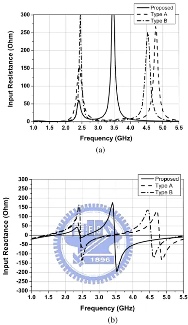
Figure 3.8 Simulated (a)input resistance and (b)reactance for the proposed, type A, and type B antennas. ...45
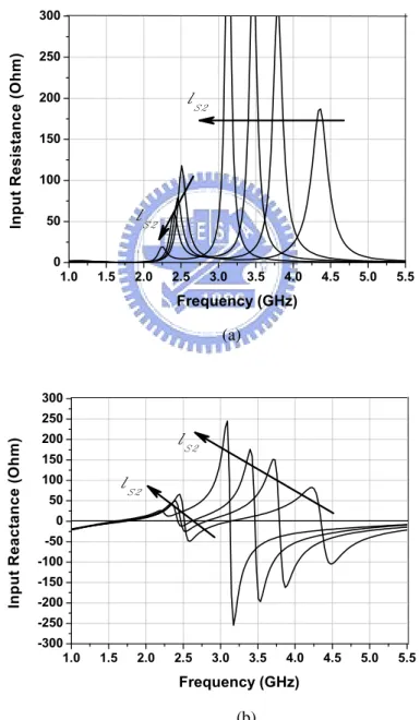
Figure 3.9 Simulated (a) real part and (b)imaginary part of the input impedance, with changing the slot length lS2 under L1, for the proposed antenna. lS2 = 1.5, 3.0, 3.5, 4.5 mm. ...46
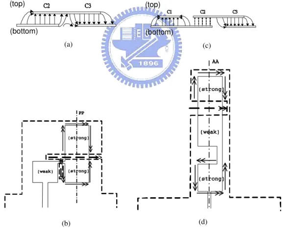
Figure 3.10 (a)Schematic for the electric field distribution at the PP cut for the proposed antenna. (b) Schematic of the equivalent magnetic current distribution for the proposed antenna. (c)Schematic of the electric field distribution at the AA cut for the type A antenna. (d)Schematic of the equivalent magnetic current distribution for the type A antenna...48 Figure 3.11 Simulated and measured return loss for (a)the proposed antenna and
(b)the type A antenna. ...49 Figure 3.12 Simulated and measured radiation patterns for the proposed antenna. ..50 Figure 3.13 Simulated and measured radiation patterns for the type-A antenna...50 Figure 3.14 (a)The realized proposed antenna layout with printed elements. (b)The
realized proposed antenna layout with lumped capacitors. (c)The measured input impedance of the antenna with printed element. (d)The measured input impedance of the antenna with lumped capacitors. (e)The measured radiation pattern of the antenna with printed element in x-z plane. (f)The measured radiation pattern of the antenna with lumped capacitors in x-z plane...52 Figure 3.15 (a)The proposed antenna configuration with different ground sizes.
(b)The return loss of the proposed antenna configuration with different ground sizes...53 Figure 3.16 (a)The configuration of an open-end slot antenna fed by a short-circuited microstrip line. (b)The corresponding equivalent circuit model. ...56 Figure 3.17 (a)The input impedance from full wave simulation with different lM.
(b)The input impedance from model calculation with different lM. ...57
Figure 3.18 (a)The configuration of a conventional microstrip-fed slot antenna with open end. (b)The configuration of the proposed slot antenna. Both the
configurations have the identical slot size. ...58 Figure 3.19 The corresponding equivalent circuit model of the antenna configuration in Figure 3.18. ...58 Figure 3.20 The comparison of input impedance between circuit model calculation
and full-wave simulation. (a)The conventional open-end slot antenna. (b)The proposed open-end slot antenna...60 Figure 3.21 The simulated and measured return losses of the proposed antenna...62 Figure 3.22 The measured radiation patterns of the proposed antenna. ...62 Figure 3.23 (a)One-eighth wavelength antennas with identical slot and capacitors
with different ground sizes. (b)The return losses of one-eighth wavelength
antennas with identical slot and capacitors with different ground sizes. ...63 Figure 3.24 The geometry of the proposed frequency tunable antenna ...65 Figure 3.25 (a)The equivalent circuit model of the proposed antenna. (b)The
Figure 3.26 The impedance curve, r(f)+jx(f), of the slot line on smith chart from the full-wave simulation. The denoted region is the forbidden area for the proposed matching scheme...67 Figure 3.27 The measured return losses of the antenna with SMD capacitors...68 Figure 3.28 Measured patterns The measured radiation patterns of different
operational frequencies (a)The antenna with C1 = 0.2 pF and C2 = 0.4 pF for
3.5GHz.. (b)The antenna with C1 = 0.6 pF and C2 = 2.2 pF for 2.45GHz. (c)The
antenna with C1 = 1.2 pF and C2 = 2.7 pF for 1.9GHz. (d)The antenna with C1 =
1.5 pF and C2 = 3.9 pF for 1.64GHz...71
Figure 3.29 The illustration of the frequency tunable antenna layout (a)Whole view (b)Circuit arrangement...72 Figure 3.30 The photograph of the realized frequency tunable antenna. ...72 Figure 3.31 The measured return losses of frequency tunable antennas using varactors with different applied voltages for different operational frequency...73 Figure 3.32 The capacitance tuning range of ALPHA SMV1232 varactor. ...74 Figure 3.33 Measured radiation pattern of frequency tunable antenna on yz-plane in
1.65GHz, 1.95GHz, and 2.45Ghz (E-total). ...74 Figure 3.34 The comparison of radiation efficiency for using capacitors and varactors.
...75 Figure 4.1 Configuration of the proposed ground edge current choke...78 Figure 4.2 (a)The transmission line structure for measuring the proposed RF choke. Ls
= 50 mm, Ws = 20 mm, w = 5 mm, and d = 1.6 mm. (b)Equivalent circuit of
measurement structure. (c)The photograph of measurement transmission line structure...79 Figure 4.3 Simulated and measured transmission coefficients for the GECC of various sizes. (a)Frequency responses for the chokes of different length a with b = 2 mm and c = 3.9 mm. (b)Frequency responses for the chokes of different width b with a = 3.5 mm and c = 3.9 mm. (c)Frequency responses for the chokes of different strip length c with a = 3.5 mm and b = 2 mm. Other structure parameters are fixed as t = 1 mm, l = 0.5 mm, and s = 0.6 mm...83 Figure 4.4 Structure of two nearby printed inverted-L antennas with a GECC in
between. ...84 Figure 4.5 Measured scattering parameters for two printed inverted-L antennas
without GECC in between. ...86 Figure 4.6 Measured scattering parameters for two printed inverted-L antennas with
GECC in between. ...86 Figure 4.7 The time-averaged current distribution on the antennas and ground plane
Figure 4.8 (a)Structure of the inverted-L monopole antenna with long ground plane. (b)Simulated and measured reflection coefficients of the inverted-L antenna. ...88 Figure 4.9 (a)Simulated and measured radiation patterns of the inverted-L antenna.
(b)Current distributions in different time steps of the inverted-L antenna at 5.25 GHz. T is the time period of the signal at 5.25 GHz. The arrows indicate the current null positions...89 Figure 4.10 (a)Structure of the inverted-L monopole antenna with GECC.
(b)Simulated and measured reflection coefficients of the inverted-L antenna with GECC...91 Figure 4.11 (a)Simulated and measured radiation patterns of the inverted-L antenna
with GECC. (b)The time-averaged current distribution combined with an instant current vector distribution on the ground plane of the inverted-L antenna with GECC...92 Figure A.1 The function blocks of the proposed decoupling structure, including two
transmission lines, a shunt reactive component, and two impedance matching networks...103 Figure A.2 (a)The coupled antennas in connection with the decoupling network.
(b)The corresponding even-mode circuit, and (c) the odd-mode circuit. ...105 Figure A.3 The configuration of the two closely spaced printed monopole antennas.
...108 Figure A.4 (a)The simulated reflection coefficient S11 and coupling coefficient S21, in
the complex plane, of the strongly coupled monopole antennas. (b)Measured and simulated return losses. (c)Measured and simulated isolations. ...109 Figure A.5 (a)The simulated reflection coefficient S11 and coupling coefficient S21, in
the complex plane, of the coupling monopole antennas with decoupling network. (b)Measured and simulated return losses. (c)Measured and simulated isolations. ... 111 Figure A.6 (a)The simulated reflection coefficient S11 and coupling coefficient S21, in
the complex plane, of the coupling monopole antennas with decoupling network and impedance matching networks. (b)Measured and simulated return losses. (c)Measured and simulated isolations... 112 Figure A.7 Measured radiation patterns of the two closely spaced printed monopole
antennas at 2.45GHz when fed from port 1: (a)x-y plane, (b)x-z plane, and (c)y-z plane... 114 Figure A.8 Measured radiation patterns (Eφ) in the x-y plane of (a)the single printed
monopole antenna and (b)the two closely spaced printed monopole antennas without decoupling. f = 2.45 GHz... 115 Figure A.9 The configuration of the two closely spaced miniaturized monopole
antennas... 116
Figure A.10 (a)The return loss and (b)the isolation of the miniaturized monopole antennas with decoupling network and impedance matching networks. ... 117
Figure A.11 Measured radiation patterns of the two closely spaced miniaturized monopole antennas at 2.45GHz when fed from port 1: (a) x-y plane, (b) x-z plane, and (c) y-z plane. ... 118
Figure A.12 Antenna layout. (a)Top view (b)Bottom view. ...120
Figure A.13 Simulated S-parameters of the two closely spaced antennas. ...120
Figure A.14 (a)The decouple network and (b)the matching network...121
Chapter 1 Introduction
1.1 Background and Motivation
In the past decade, wireless communication has grown rapidly. Many systems have been widely used, e.g. Global Position System (GPS), Wi-Fi for Wireless Local Area Network (WLAN), WiMAX, Bluetooth, and Global System for Mobile Communication (GSM) and Digital Cellular System (DCS). As these systems gain popularity, the demand for wireless products has highly increased, particularly for mobile devices. With the rapid development of the integrated circuit technology, the wireless mobile devices tend to be compact and integrated with multiple systems. For example, a USB WLAN card today is only typically 12 mm × 50 mm that is smaller PCMCIA ( 50 mm by 100 mm ) (λ0/4 of 2.4GHz is 32.5 mm). Also, more
than one wireless system is evident inside a smart phone today, e.g. GSM, Bluetooth, GPS, WiFi. Moreover, for increasing the data through put, the multiple-input multiple-output (MIMO) antenna system was developed. The system employs multiple antennas which simultaneously transmit and receive within the same system. These examples have to integrate multiple antennas in one device. As a result of the increased demand for miniaturized wireless devices, compact antenna designs with high integrating ability are desired. Since the small devices have limited space reserved for antennas, size reduction becomes the primary concern [1]. Antennas have to be arranged closely giving serious coupling issue in application. However, the coupling will be a serious problem in applications. Therefore, antenna design in modern wireless products has to face important issues on miniaturization and decoupling [2]-[4].
This dissertation focuses on the development of miniaturized antennas and the isolation enhancement between closely-spaced antennas. There are already many design methods for miniaturized antennas – most of which utilize the structure natural resonance of the structure (which corresponds to the length of the antenna). Most miniaturization designs can be simply categorized into three groups – bending the
capacitance in single a LC resonator.
Metamaterial have recently bacomes popular in antenna design. There have been many published designs on this subject but the input matching or radiation mechanisms are usually not discussed. A survey of these designs will be discussed in the next section. This dissertation tries to develop a new design method of compact antennas and to provide the equivalent circuit analysis for demonstration. The design methodology stems from equivalent circuit analysis to synthesize the resonance and process input matching. This design concept aims to diminish the consideration of wavelengths. As such, the compact antenna size is possibly smaller if resonance is achieved by discrete reactive elements in stead of the physical length. This dissertation will also study the conventional designs of bending the resonant path and dielectric loading.
The coupling between antennas will degrade the communication system performance, in terms of efficiency due to the cause of power dissipated because of coupling. The solution to this problem is to prevent the other antennas from absorbing the power. In this case, the antenna will be a reactive element with current on it but without power dissipation. This can be achieved by increasing the isolation between antenna terminals, i.e. increasing port isolation. Another solution is to decouple antennas for no current distribution on inactive antennas. Both conditions have already been discussed widely. A survey for above methodology will be presented in the next section. However, many of today’s published designs are bulky and most of them are not flexible enough for practical applications.
Today’s antennas tend to be compact and so does the decoupling structure for smaller devices. Therefore, this dissertation proposes two compact designs for decoupling and port isolation enhancement. The port isolation enhancement design can process two very closely-spaced antennas. The miniaturization methods of decoupling that respond to the miniaturized antennas also use the circuit approach design for size reduction.
1.2 Literature Survey
In this section, the conventional miniaturization designs and decoupling methods will be presented briefly. The miniaturization methods introduced here are divided into three parts: 1. resonant path alignment, inductive loading or capacitive loading, 2. dielectric loading, and 3. using metamaterial. In the first section, some compact printed dual-band design will also be mentioned due to their popularity.
1.2.1 Miniaturized Antennas
Most compact antennas are resonant antennas. In resonant type wire antennas, length is a main factor in determining the antennas’ frequency of operation. For a conventional monopole, it requires a quarter wavelength to resonate and for a loop antenna, it requires one wavelength. To have a compact design, one can simply arrange the resonant path inside a small area or reduce the physical length by inductive or capacitive loading while keeping same electrical length. The conventional design of the resonant path alignment is to bend, fold or turn the path into a smaller size – even a spiral or helical shape is acceptable. Figure 1.1 shows a loop antenna that is folded to be compact for handset application [1].
For mass production, cost is always the first priority. The following examples are given with low cost printed antennas. The printed slot antenna consisting of a slot line, can be miniaturized using similar methods. For example, the most used method is to spiral the slot while keeping its resonant length as shown in Figure 1.2 [5]-[7]. In Figure 1.2(b), a compact open-ended meander slot antenna is shown [8]. In Figure 1.1(c) a slot ring has been miniaturized by fractal geometry [9]. The length of these spiraled or meandered slots have been effectively reduced by increasing antenna width. By bending the slot, the above methods have maintained the total electrical length which determine the resonant frequency.
According to transmission line theory, the inductive loading or capacitive loading can increase the equivalent electrical length which is useful in miniaturizing
capacitive loading, as realized by printed elements, shown in Figure 1.3(a) [10]. Chip capacitors can be loaded at the ends of the coplanar-waveguide-fed slot line for further size reduction, as shown in Figure 1.3(b) [8]. Figure 1.3(c) is the disk-loaded monopole. The antenna is considered as a series LC resonator when the disk acts as a capacitive load [11]. The simple LC model can show resonance characteristics of an antenna but does not include an impedance matching mechanism.
Aside from, a single-band compact antenna, there are many other compact dual-band antenna designs. Since 1999, the WLAN standards including the IEEE 802.11a/b/g systems were established by the IEEE 802.11 Group. In the U.S., the 802.11b/g WLAN standards are used in the frequency range of 2.4 to 2.4835 GHz while the 802.11a standards are used from 5.15 to 5.35 GHz and 5.725 to 5.825 GHz. To enhance the communication capacity of a unit cell, a combo system with 802.11a/g or 802.11a/b/g standards have became popular. In this combo system, the antennas are like transceivers operating in both 2.45 and 5.25 GHz frequency bands; thus, a dual-band antenna with a single input port is needed for size reduction. Many dual-band antennas have been proposed in the literatures. Some of these designs use two similar resonators to achieve dual-band operations, such as a double inverted-F antenna [13] and an F shape monopole (double-L monopole), as shown in Figure 1.4(a) [14]-[17]. These are miniaturized by bending the strips into an L-shape. Also, some of these designs use a single block antenna with multiple resonant modes to achieve dual-band operations, such as a tapered bent folded monopole [18], as shown in Figure 1.4(b), meandered CPW-fed monopole [19], and, an L-shaped monopole [20].
Figure 1.1 Line alignments of a loop antenna for handset use.
(a) (b) (c)
Figure 1.2 (a)The spiraled microstrip-fed slot antenna. (b)The microstrip-fed meandered slot antenna. (c)The fractal microstrip-fed slot ring antenna.
(a) (b) (c)
Figure 1.3 (a)The microstrip-fed slot antenna with inductive load in central portion. (b)The CPW-fed slot antenna with capacitive load at the open end. (c) The disk-load monopole antenna.
20 mm 8 mm 24 mm 19 mm 24 mm 19 mm Feed Feed (a) (b)
Figure 1.4 (a)The compact coupled inverted-L dual-band antenna. (b)The compact CPW-fed dual-band antenna.
(a) (b)
Figure 1.5 (a)The monopole antenna printed on a dielectric slab. (b)The dielectric loaded monopole antenna.
To have enough electrical length under physical constraints, employing the use of a dielectric is an efficient solution. With a material of higher relative permittivity, one can have a larger phase constant, thereby reducing the physical resonant length [21]. Figure 1.5 shows a monopole printed on a ceramic piece [22]-[23]. In Figure 1.5(b) the antenna length is half than that in air by using the relative permittivity of 22 [23].
Unlike natural transmission line with a positive phase constant, metamaterial based transmission lines have a designable phase constant. This kind of artificial structure has been utilized by numerous guided and unguided wave applications. One notable example is Left-handed materials (LHMs) which possess negative refractive index and have drawn tremendous interests in both scientific and engineering fields. The Left-handed transmission line (LH TL) is characterized by the phase advance whereas the Right-handed transmission line (RH TL) is characterized by phase delay along the power traveling direction. Metamaterial antennas possess different characteristics from conventional antenna designs that are based on the standard transmission line. RH TL and LH TL can be embedded into each other and named as Composite Right/Left- Handed Transmission Line (CRLH TL). [24] provides an practical application inserting LH TL into the host RH TL. Its equivalent circuit and phase constant are shown in Figure 1.6. The Zeroth-order Resonance (ZOR) makes use of the opposite phase properties of RH and LH TL and has been proved experimentally [25]. Small planar antennas utilizing the ZOR structure were published [26-27], as shown in Figure 1.7. Basically, they are just a section of synthesized CRLH TL. The physical size of such antenna can be arbitrary since its size is specified by the value of the capacitances and inductances instead of wavelength. The concept of the infinite wavelength resonant antenna was first demonstrated in [26].
(a) (b)
Figure 1.6 (a)The equivalent lumped circuit of CRLH TL. (b)The phase constant curve of CRLH TL which possesses both positive and negative values.
Feed
CRLH TL
(a) (b)
1.2.2 Decoupling Methods
The use of multi-element antennas, such as MIMO antenna systems, is one of the effective ways to improve reliability and increase channel capacity. Due to the sharing of ground currents between antennas, these antennas couple strongly to each other; thereby, making it difficult to integrate multiple antennas closely in a small and compact mobile handset. For an MxN MIMO communication system, the data throughput can be pushed up to K times ( K = min(M, N) ), that of a Single-Input Single-Output (SISO) system, as long as the communication channels linked between the transmitter and the receiver are uncorrelated [2][3][29]. The correlation between the channels depends not only on the propagation environment, e.g., multi-path effect due to the reflection and diffraction of outdoor buildings or indoor partitions, but also on the coupling between the M or N antennas. High antenna coupling (or low isolation) would introduce signal leakage from one antenna to another, thus increasing the signal correlation between the channels. It will also decrease the antenna radiation efficiency due power dissipated in the coupled antenna port. The signal correlation between two receiver antennas can be reduced by increasing the antenna spacing. However, spacing is usually limited, especially for a mobile terminal which has very strict volume reserved for antennas. Another way to diminish correlation is by using multiple antennas with different radiation patterns. The patterns have to be complementary to each other in space in order to receive multi-path signals from various directions. However, the complementary patterns may not be the best solution for MIMO system. This is because for a single device, aside from the MIMO system, there are other systems operating simultaneously in the same frequency band, e.g. IEEE 802.11b and Bluetooth – both of which are popular systems that operate in the same 2.45GHz band. In this case, the coupling problem causes the same problem as MIMO system of the radiation efficiency. Thus, it causes inefficiency in the systems due to coupling.
Currently, there are numerous papers published focus on diminishing antenna coupling. Itoh and his co-workers used the defected ground structure (DGS) to increase the port isolation of dual-polarized and dual-frequency patch antennas [30]
same frequency electromagnetic band gap (EBG) structures can be used. Inserting band gap structures between antennas can help block wave coupling. Mushroom-like EBG structures are usually inserted between patch antennas to prevent the propagation of surface waves for higher isolation and better radiation patterns, as shown in Figure 1.8 [31]-[32]. These EBG structures provide conspicuous decoupling effect, but suffer from complicated structures and large structure area. Possible loss may also be induced in the resonant EBG structures. To reduce the coupling between two planar inverted F antennas (PIFAs), Diallo [33]-[36] used a suspended metal strip linking the two antennas to cancel the reactive coupling between antennas, as shown in Figure 1.9. This neutralization technique has been also extended to patch antennas by Ranvier [37]. In [38], a decoupling circuit network was realized for two-element array by using external transmission lines. Although good isolation was achieved, only weak coupled antennas were tackled. The all-transmission-lines configuration also made the circuit bulky. The mutual coupling of two closely-packed antennas was reduced by etching slots on the ground plane [39]. The fish-bone like slots formed equivalent inductors and capacitors on the ground plane, which prevented the flowing of the coupling ground current between the antennas, as shown in Figure 1.10. A large ground plane size, which was close to the antenna size, was needed for sufficient isolation. The above methods can be divided into two cases. The first is to insert band gap structures prevent the direct propagation of electromagnetic wave between two antennas, like EBG and DGS. The driven antenna will not induce current on the other antenna. The second is to cancel the coupling current by using additional reactance network between antenna ports, such as a suspended strip, as a decoupling network. This is similar to the crosstalk elimination circuit used in telephone network. In this case, the driven antenna does induce the current on the other antenna but the decoupling network cancel the current at the antenna terminal.
In conclusion, most of the decoupling technology are bulky, especially EBG structure. The suspended reactive element between antennas is simple but not convenient for the application due to the additional empty space requirement and wire supporting mechanism. These designs are not flexible and compact enough for different PCB configurations. Therefore, this dissertation would like to propose a
more compact and flexible method for decoupling. The primary consideration for their design is to attain a compact size followed by system flexibility.
EBG wall Patch antenna
Ground
Figure 1.8 The EBG structure used to decouple two patch antennas.
Feed Shorting pin
PIFA
Suspended reactive element for decoupling
Ground
Monopole 1 Monopole 2
Fish-bone like structure Ground
Figure 1.10 A fish-bone-like structure inserter on the ground plane to decouple two monopole antennas.
1.2.3 Antenna Equivalent Circuit Analysis
The equivalent circuit analysis is a kind of antenna modeling, which uses a lumped element circuit to model the input impedance of an antenna. Therefore, the equivalent circuit approach used in this study uses a lumped element circuit for antenna analysis and design.
The equivalent circuit analysis of antennas has already been used for decades. This method is usually used to explain antenna impedance and resonance mechanisms [40]-[43]. Additionally, the equivalent circuits of antennas are used in spice modeling for the analysis of antenna gain bandwidth or time-domain waveforms transmitted from antennas, etc [44]-[45].
Circuit models are used to represent antenna impedance curves. Thus, their creation usually considers antenna physics which mostly relate to resonance mechanisms. For example, a loop antenna with an anti-resonance at the operating frequency will be basically modeled by a parallel LC resonator. A parallel resonator is a basic circuit model of antennas with anti-resonance. However, a purely parallel resonator cannot depict antenna impedance curves precisely. Additional circuit parameters, such as parasitic capacitors, are required for better modeling.
Another topic relevant to equivalent circuit modeling is effective modeling bandwidth. Since lumped elements have bandwidth limitations for modeling distributed elements, the circuit model with lumped elements is also limited; thus, to describe antenna impedance over a wider bandwidth by circuit elements, distributed elements, such as a transmission line will be used.
[40], shows an antenna equivalent circuit of a strip line coupled patch antenna that considers many circuit parameters. Figure 1.11 shows the presented antenna equivalent circuit in [40]. Considering the anti-resonance of the patch antenna, RA, LA,
and Cp basically form the parallel resonator of a patch. To increase modeling
accuracy, LP and RP are treated as parasitic elements connected in series with Cp.
Coupling through the slot of an open-ended strip line are represented by an impedance transformer – Ct and Lt. The circuit elements mentioned above form a complex
antenna equivalent circuit model. The value of each circuit element can be obtained by curve fitting. Therefore, knowing the antenna input impedance is necessary for model extraction regardless of where this value is obtained – whether from measurement or from full-wave simulation. Another example on the operation mechanism of an antenna is that of a ladder CPW-fed slot antenna using multiple resonators. [41] shows a circuit model to explain and describe resonances of such an antenna. This type of circuit modeling does not have a direct relation with antenna
resonators are used to precisely fit the antenna impedance curve over a wider bandwidth since the two resonators can provide two additional poles, thereby, increasing flexibility in curve fitting.
The equivalent circuit is not only used to explain the operation mechanism and describe the impedance curve but is also for spice simulation in the time domain. In [44], a circuit model of an ultra-wide-band antenna is established and is used to calculate the waveform of receiving signal. Chapter 2 of this dissertation will show the equivalent circuit analysis for the proposed antenna structures.
(a) (b)
Figure 1.11 (a)A stripline coupled patch antenna (b)The equivalent circuit model of a stripline coupled patch antenna.
1.3 Antenna synthesis by the Equivalent Circuit Approach
In most publications, the antenna equivalent circuit is used for analysis and explanation. Design of the antenna is usually done first and then the establishment of equivalent circuit. However, the use of the antenna equivalent circuit can be expanded to antenna design. This means that the equivalent circuit must be designed first then synthesized into the antenna design. Chapter 3 will shows the synthesis of an antenna from an equivalent circuit.
This study uses the equivalent circuit approach to achieve miniaturized design. An equivalent circuit established prior to achieve resonance at the antenna’s operation frequency. The antenna is directly synthesized from the equivalent circuit instead of the iterative full wave simulation analysis. The equivalent circuit is designed to create resonance at a specified frequency. This is used as a reference in antenna synthesis. Next, the antenna topology is mapped from the equivalent circuit by using printed circuit elements to represent components of the circuit model. In this design procedure, resonant frequency can be easily controlled by an equivalent circuit. However, the radiation effect of antenna is difficult to control in the equivalent circuit model. To solve this problem, there are two possible methods. The first method uses equivalent circuits to control the resonance type and resonant frequencies of antennas. The bandwidth and radiation performance need to be fine tuned when processing the antenna layout. This means the radiation mechanism is considered during layout. This design method will be shown in Chapter 3-1.
The second method establishes circuit model of radiators by considering the radiation mechanism, and radiation resistor, during modeling. This means certain basic radiators, such as slots, should be modeled first. Thus, some preparatory work has to be done before the design of antenna equivalent circuit, such as establishing the radiator model library. The radiator model can be obtained through full-wave simulation or by measurements. However, only simple radiators can be modeled very well. Additionally, interaction between multiple radiators of the same antenna is also very difficult to be modeled. This method will be shown in Chapter 3-2.
The method of antenna synthesis from equivalent circuit model increases the flexibility of antenna design and reduces simulation efforts. Basic antenna design needs several iterations of full-wave simulation in order to obtain the specified resonant frequency followed by antenna layout tuning for input matching and bandwidth. The equivalent circuit approach helps obtain the correct resonant frequency quickly. For radiator models, although it takes time for modeling, the obtained radiator model can be reused in many future antenna designs.
1.4 Contributions
A series of miniaturized antenna design is presented with the equivalent circuit analysis. Also, the decoupling methods for two closely-space miniaturized antennas are developed. Both of miniaturized antenna design and decoupling method are important in modern wireless applications because modern devices tend to be smaller with less reserved antenna space. Antenna designs or decoupling structures should therefore be more compact as compared to whole device.
The research of miniaturized antennas is divided into two categorizes. One category is to use natural resonance in design – resonant antenna by using wavelengths. The other is design by circuit approach – creating resonance irrespective of wavelength. In the first category, a printed spiraled inverted-F antenna operating in 2.4/5.2GHz is very compact (9.5 mm by 6.5 mm). This can easily fit in most compact devices today. The dual-band mechanism of the spiraled inverted-F antenna is also explained by the equivalent circuit model. The dielectric-loaded quadrature helix antenna (QHA) with relative permittivity of 40 is another compact antenna design which is only 2.7% of air-loaded antenna. The challenge and solution of using dielectric to miniaturize QHA is studied and demonstrated in this dissertation. Two designs using circuit approach are proposed. The first design uses a short slot radiator with cascaded left/right-handed transmission line feed. The use of two cascaded sections of transmission line with identical electrical length and opposite phase constant to create anti-resonance is new concept. The second design uses a short slot radiator as an inductive element and two capacitors for tuning resonant frequency and matching. Both designs are with equivalent circuit demonstrations to help understand the antenna impedance and operating principle of the antenna. The advantages of circuit approach design are the flexibility and compactness of the resulting design which can be merged to the design of the wireless communication system. The radiation mechanism and input impedance are also discussed in the above design. The miniaturization methods mentioned provide new design concepts, several techniques and complete impedance analysis for compact antenna design.
The decoupling design reveals two compact structures. One is the circuit approach design which can reduce coupling by the circuit and can handle any two
closely-spaced antennas. The complete analysis of the circuit structure is demonstrated in Appendix A. Additionally, the same structure can be extended to dual-band application under limited conditions. The other is the miniaturized current choke that can block ground edge current. The ground edge current effect is common in monopole antenna design. The proposed choke was developed against edge current. Two useful applications are presented – decoupling and pattern regulation. The current distribution analysis is also illustrated to help understand the behavior of the edge current and the current choke. Both miniaturized decoupling structure are compact and flexible for application. This dissertation focuses on the miniaturization design of antenna and decoupling structures.
Chapter 2
Miniaturized
Antennas
with
Wave
Resonances
2.1 Spiraled Printed Inverted-F Antenna
The conventional printed inverted-F antenna is widely used because of several advantages such as making up with ease, matching the input impedance with no outer circuit, having omni-directional pattern, etc. However, its length is limited to be a quarter wavelength of the operating frequency, which usually occupies quite a few amounts of space in PCB [46]-[49]. Besides, the single inverted-F antenna can only be operated at the certain resonant frequency, which is unable to supply the market need of dual-band or triple-band applications. To solve these problems, in this section, PIFA related structures by means of spiraling an inverted-F antenna which achieves dual-band operation by one resonator. The antenna is designed on the FR4 substrate with 0.8mm thickness for commercial usage.
2.1.1 Antenna Configuration
via
h
l
H
W
y
x
w
sl
sg
Figure 2.1 The configuration of dual-band spiraled printed inverted-F antenna.
The first PIFA-related miniaturized dual-band antenna is the spiraled PIFA (Figure 2.1). The spiral inductor loaded on the antenna can both realize dual-band
operation and miniaturizes the size of the conventional inverted-F antenna. The chosen ground width is 46 mm compatible for PCMCIA interface. The antenna placed near the edge of ground plane is possible for antenna diversity.
2.1.2 Equivalent Circuit Analysis
In this section, the effect of the spiral is discussed and the circuit model is also developed for analyzing. And in Figure 2.2(a), there is a typical inverted-F antenna implemented on a printed circuit board. For this inverted-F antenna, the microstrip feed line is connected to a horizontal metal line with one end short-circuited to the ground and the other end open-circuited. The metal line and the ground plane form a quasi transmission line. It is easy to derive that as the total length of this quasi transmission line equals a quarter of wavelength, the input reactance vanishes due to the resonance of the inductor-like short-circuited line and the capacitor-like open-circuited line. The corresponding return loss simulated by the commercial EM simulator IE3D [50] is presented as the curve a in Figure 2.3(a). Here, the length of the horizontal metal line is designed as a quarter wavelength of the fundamental frequency 2.45 GHz, so that a deep resonance occurs at that frequency with return loss larger than 20 dB. It is noticed that another resonance presents at the frequency around 7.35 GHz, which is the triple of the fundamental frequency.
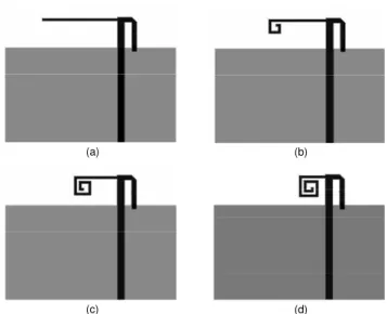
In order to demonstrate how the spiral works, a number of spiraled inverted-F antennas were also simulated. A set of spiraled inverted-F antennas (as Figure 2.2(a)-(d).) with the total length of the metal line kept similar and spiraled gradually were designed. The total length of the strip from short point to open end in Figure 2.2(a) is 25.5 mm. The fundamental resonant frequency of these antennas should remain about the same, which can be verified from the simulated return losses shown in the curves a-d of Figure 2.3(a). As a matter of fact, the return losses of the four antennas are all better than 15 dB, except for the variation of the bandwidth. However, it is also found that the frequency of the second resonance becomes lower as the antenna tail is spiraled more. The second resonant frequency shrinks to about 71% (from 7.35 to 5.25 GHz) when the antenna structure is changed from the conventional PIFA of Figure 2.2(a) to the spiraled one of Figure 2.2(d).
(a) (b)
(c) (d)
Figure 2.2 Four printed inverted-F antennas with different spiraled tails. The tail lengths are kept the same for the four antennas.
1 2 3 4 5 6 7 8 9 R et u rn L o ss ( d B ) 25 20 15 10 5 0 a b c d Frequency (GHz) 0 (a) 2.2 2.3 2.4 2.5 2.6 2.7 Frequency (GHz) 50 60 70 80 90 100 A n te n n a E ff ic ie n c y ( % ) a b c d (b)
Figure 2.3 (a)Simulated return losses, as functions of frequency, for the antennas shown in Figure 2.2. (b)Simulated radiation efficiency, as functions of frequency, for the antennas shown in Figure 2.2.
The miniature antenna always encounters the problem of the efficiency, especially for the lower operation band. The simulation of antenna efficiency around 2.45GHz is shown in Figure 2.3(b). It can be found that the efficiency is almost the same (about 70%) for the four antennas shown in Figure 2.2. The degradation of efficiency is under 5% in the required bandwidth. It means that the additional loss induced in this miniaturized antenna design is negligible. The invariance of the efficiency may be due to that a large ground plane with length larger than a quarter wavelength is used. (Note that the ground plane is a part of the antenna, on which the induced current contributes to the radiation performance of the antenna.) However, the bandwidth of the 2.45GHz band shown in Figure 2.3(a) becomes narrower with the smaller antenna size. This can be attributed to the increasing of antenna quality factor due to the antenna size. The efficiency of the well matched spiraled inverted-F antenna around 5.2GHz is about 50%, which is lower than that (70%) of a typical PIFA designed at the same frequency. In the 5GHz band, the proposed antenna operates at the high order mode with three quarter wavelength resonance. The current flows in the spiral with different directions, thus reducing the radiation efficiency of the antenna.
For conceptually understanding the frequency reduction effect of the second resonance, a brief equivalent circuit model for the spiraled PIFA is proposed as shown in Figure 2.4(a), where the PIFA is modeled as a short-circuited transmission line of length θ2 in shunt with a transmission line of length θ1 loaded by an effective radiation
resistance Ra. An inductor L is inserted in the end of the open-circuited transmission
line in order to take account of the spiraling effect of the antenna tail and the parasitic inductance of the transmission line. In addition, a parasitic capacitor Cs shunt to
ground for fringe field is considered in the open-end transmission line. The input admittance 2 0 1 0 1 0 0 2 1 cot tan tan θ θ θ jY jY Y jY Y Y Y Y Y L L in − + + = + = (2-1)
where Y0 (= Z0-1) and β denote the characteristic admittance and phase constant,
respectively, of the transmission line. The admittance YL can be written as:
+ + = = − s a L L jwC R jwL Z Y 1 1 (2-2)
0 0 in in Y Y Y Y − Γ = + . (2-3) Feed
R
aL
C
s Zo,ΘΘΘΘ1 Zo, ΘΘΘΘ2 Y 2 Y 1 Y L (a) S 1 1 (d B ) 1 2 3 4 5 6 7 8 9 Frequency (GHz) -25 -20 -15 -10 -5 0 a b c d (b)Figure 2.4 (a)Equivalent transmission line model for the spiraled printed inverted-F antenna. (b)Simulated return losses of the equivalent model with Zo = 180 Ω, θ1 = 57.4
o
, θ2 = 18.3 o
, Cs = 0.13 pF,
Ra = 150 Ω and L = 3.7, 6, 8, 12nH.
Figure 2.4(b) illustrates the calculated return losses, functions of frequency, for the equivalent circuit model of the spiraled antenna. The characteristic impedance Zo is
180 Ω, which is about the EM-simulation value of the characteristic impedance for the antenna’s quasi transmission line portion. The electrical length is set as θ1 = 57.4 o
and θ2 = 19o at 2.45GHz. The total electrical length is around quarter wavelength at
2.45GHz. Consider the small parasitic capacitor Cs to be 0.19pF as fringe field. The
effective radiation resistance Ra is around 150 Ω. The inductor L is related to the
spiraled strip, which is the dominant factor of the model. From the intuition, its value should increase as the strip is spiraled more. However, since the inductance
caused from the spiraling is distributed in the structure, it is hard to extract from the EM simulation. In this study, this inductor was chosen as 3.7, 6, 8, and 12 nH for the antennas (a) to (d) in Figure 2.2, respectively, so as to fit the EM-simulation results (Figure 2.3 (a)) of the antennas.
One can observe from Figure 2.4(b) that in the frequency span, two resonances are generated by each circuit. The higher resonant frequency at 7.35 GHz moves towards the lower frequencies of 6.5, 6, and 5.25 GHz, although, at the same time, the lower resonant frequency is remained around 2.45 GHz. Finally the specified dual-band operation is achieved by only one resonator. The results resemble those of the spiral antennas quite well, meaning that the equivalent circuit model including the value-changing inductor does explain the frequency characteristics of the proposed dual-band antennas.
2.1.3 Experimental Results
The spiraled PIFA of Figure 2.2(d) (or Figure 2.1) was fabricated on an FR4 (εr =
4.4) substrate with thickness 0.8 mm. The ground size of the substrate is set as W × H = 46 mm × 55 mm. The antenna occupies an area of l × h = 9.5 mm × 6.5 mm, which is only 50% of that of the PIFA without spiraling. The others parameters are ls=4.5 mm, ws=4 mm, g=1.54 mm and both the width and gap of spiral=0.5 mm.
Figure 2.5 shows the measured return loss corresponding to the EM simulated one. Both results agree each other quite well. The measured 10-dB bandwidth is 140 MHz centered at 2.45 GHz and 756 MHz at 5.25 GHz.
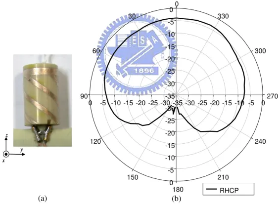
The measurement radiation patterns of the antenna are presented in Figure 2.6(a) for 2.45 GHz and Figure 2.6(b) for 5.25 GHz. Comparing with the conventional antenna (not shown here), the radiation patterns at the lower frequency of the proposed spiraled antenna are not varied much. The radiation pattern in the y-z plane is omni-directional with a peak gain of 1.59 dBi and average gain about -3 dBi. The radiation patterns at 5.25 GHz are also omni-directional in the y-z and x-z planes. The peak gain and average gain are respectively near 3 and -1.5 dBi in the y-z plane, and are about 0 and -5 dBi in the x-z plane.
Frequency (GHz)
2 3 4 5 6 25 20 15 10 5 0 2 3 4 5 6R
et
u
rn
L
o
ss
(
d
B
)
20 7 7 Simulation Measurement 7 7 Simulation MeasurementFigure 2.5 Simulated and measured return losses to frequency of the dual-band spiraled printed inverted-F antenna. 2.45GHz x_y plane -35 -30 -25 -20 -15 -10 -5 0 5 -35 -30 -25 -20 -15 -10 -5 0 5 -35 -30 -25 -20 -15 -10 -5 0 5 -35 -30 -25 -20 -15 -10 -5 0 5 0 30 60 90 120 150 180 210 240 270 300 330 2.45GHz x_z plane -35 -30 -25 -20 -15 -10 -5 0 5 -35 -30 -25 -20 -15 -10 -5 0 5 -35 -30 -25 -20 -15 -10 -5 0 5 -35 -30 -25 -20 -15 -10 -5 0 5 0 30 60 90 120 150 180 210 240 270 300 330 2.45GHz y_z plane -35 -30 -25 -20 -15 -10 -5 0 5 -35 -30 -25 -20 -15 -10 -5 0 5 -35 -30 -25 -20 -15 -10 -5 0 5 -35 -30 -25 -20 -15 -10 -5 0 5 0 30 60 90 120 150 180 210 240 270 300 330 Eθ: Eφ: Eθ: Eφ: y x (a)
5.25GHz x_y plane -35 -30 -25 -20 -15 -10 -5 0 5 -35 -30 -25 -20 -15 -10 -5 0 5 -35 -30 -25 -20 -15 -10 -5 0 5 -35 -30 -25 -20 -15 -10 -5 0 5 0 30 60 90 120 150 180 210 240 270 300 330 5.25GHz x-z plane -35 -30 -25 -20 -15 -10 -5 0 5 -35 -30 -25 -20 -15 -10 -5 0 5 -35 -30 -25 -20 -15 -10 -5 0 5 -35 -30 -25 -20 -15 -10 -5 0 5 0 30 60 90 120 150 180 210 240 270 300 330 5.25GHz y-z plane -35 -30 -25 -20 -15 -10 -5 0 5 -35 -30 -25 -20 -15 -10 -5 0 5 -35 -30 -25 -20 -15 -10 -5 0 5 -35 -30 -25 -20 -15 -10 -5 0 5 0 30 60 90 120 150 180 210 240 270 300 330
E
θ:
E
φ:
E
θ:
E
φ:
y x (b)Figure 2.6 Measured radiation patterns at the principal planes for the dual-band spiraled PIFA at (a)2.45GHz and (b)5.25GHz. (solid line denotes E-theta; dashed line denotes E-phi)
2.1.4 Summary
Through the features of the conventional PIFA, the original antenna is re-shaped to a spiral structure for the purpose of miniaturization and dual-band operation. A dual- band equivalent circuit model for spiraled antenna has been developed as well in order to examine the effects with the tail of the antenna spiraled little by little. The size of the proposed spiraled antenna is about 50% of a conventional one. The proposed type not only holds most of the properties of the conventional antenna but also provide more options for dual-band antenna designs. Finally, since the bandwidths of the higher band is about 700 MHz, it is easy, after upwards shifting the center frequency, to cover all signal frequencies (from 5.15 GHz to 5.825 GHz) of the IEEE 802.11a WLAN application.
2.2 Dielectric-loaded Quaduature Helix Antenna
The resonant quadrifilar helix antenna (QHA) can generate a semi-spherical radiation pattern for circular polarization. This radiation pattern with a wide beamwidth can facilitate low-elevation reception or a wide angular receiving range. This antenna is already applied in many spacecraft systems [51]. The advantages of the semi-spherical radiation pattern of the QHA are also attractive for mobile satellite communication and position-location systems, which typically require circular polarization and a wide beamwidth. The conventional resonant QHA has two resonant bifilar helix antennas (BHAs) oriented in a mutually orthogonal relationship on a common axis. The resonant BHA can be treated as a twisted one-wave-length loop antenna. To achieve circular polarization, these two BHAs are fed in quadrature phase. The radiation pattern shape of the resonant QHA depends on helix dimensions, number of turns and pitch angle. When four arms are roughly half wavelength with half turn with axial length equal to a quarter wavelength, the radiation pattern approaches a semi-sphere like a cardioidal shape [52]. The demand for global positioning systems (GPSs) has recently grown dramatically for portable tracking devices or mobile phones with GPS functions. This need has led to the increased requirement for circular-polarized antennas. The good radiation property of resonant QHAs has drawn considerable attention. However, the half wavelength of 1.575GHz (GPS L1 frequency) for a resonant QHA is too long to be integrated into handsets
2.2.1 Antenna Configuration
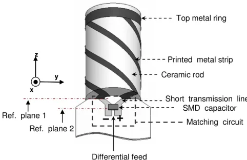
SMD capacitor Printed metal strip Ceramic rod x y z x y z Matching circuit Ref. plane 1 Ref. plane 2
Top metal ring
Short transmission line
Differential feed
Figure 2.7 Antenna structure including the adapted PCB with a SMD capacitor.
Figure 2.7 presents the geometry of the proposed antenna. The overall structure contains a hollow ceramic rod with printed metal strips on the surface and a planar circuit substrate with a matching structure and feeding lines. The ceramic rod with a relative permittivity of 40 helps reduce antenna size [53]-[54]. Its low material loss with loss tangent lower than 0.0001 at the frequency under 5GHz also helps maintain the antenna efficiency. The hollow structure of the rod is designed for fabrication convenience and to retain structure strength. The circuit substrate, which has a protrusion, can be inserted into the ceramic rod during assembly. The metal strips on the ceramic rod surface are silver ensuring good conduction, and are printed by using the low-cost screen-printing technique. To reduce the procedure of manufacture, only the rod sidewall and bottom are printed. A metal ring on the top of the sidewall is used to connect the four helical arms of the resonant QHA. The feeding lines are a differential line that directly contacts antenna feed points on the ceramic rod bottom. Feeding lines are printed on the circuit substrate. The proposed antenna is designed to operate at 1.575 GHz for GPS applications. The structure is simulated using the full-wave simulation tool, Ansoft HFSS. Due to the high permittivity of the ceramic rod, the antenna is very small, only 4.5 mm in radius and 14.8 mm in height (<0.08λ0).
The helical arms are roughly half turns with a pitch length of 22 mm. The helical orientation of the antenna affects radiation performance. The helical arms of the antenna are designed in a left-hand orientation to optimize the right-hand circular polarization (RHCP) gain in the upper half space. This helix orientation generates better RHCP gain in the upper space than a left-hand circular polarization (LHCP) gain in the lower space [52]. The antenna is matched to 100 Ω by the matching structure. The 100-Ω differential line is then used to feed the antenna. Both the feeding line and matching structure are printed on an 0.8-mm-thick FR4 substrate.
2.2.2 Equivalent Circuit Analysis and Matching Network
The impedance characteristics of the dielectric-loaded QHA can be observed from simple equivalent circuits. Because the configuration of BHA is constructed as a twisted pair line, the BHA model consists of a differential transmission line and resistor (Figure 2.8(a)). The characteristic impedance of the transmission line in the model is approximately 65 Ω. This value is similar to the simulated characteristic impedance of the twisted line in a BHA. The resistor includes the effects of radiation resistance and ohm resistance, whose value equals 1.3 Ω (obtained by curve fitting compared with full- wave simulation.) The high permittivity of the ceramic rod makes the antenna very small as compared with the wavelength in free space, and decreases radiation resistance dramatically. The small radiation resistance means that the loss tangent of the ceramic rod becomes very critical to antenna efficiency.
L1 L2 RA L1 Antenna feed Antenna feed RA RA (a) (b)
Figure 2.8 (a)The equivalent circuit of the proposed BHA. (b)The equivalent circuit of the proposed QHA.
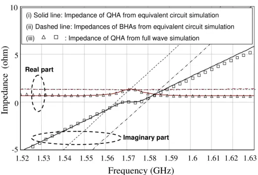
1.52 1.53 1.54 1.55 1.56 1.57 1.58 1.59 1.6 1.61 1.62 1.63 Frequency (GHz) -5 0 5 10
(i) Solid line: Impedance of QHA from equivalent circuit simulation (ii) Dashed line: Impedances of BHAs from equivalent circuit simulation (iii) : Impedance of QHA from full wave simulation
Im p ed an ce (o h m ) Real part Imaginary part
Figure 2.9 Impedances from full-wave simulation and equivalent circuit simulation.
A resonant QHA can be considered as two resonant BHAs arranged orthogonally with quadrature-phase excitation. To simplify the feeding network, the phase quadrature is obtained using the self-phasing method such that only one set of feeding lines is required. By this method, two BHAs are fed in parallel (Figure 2.8 (b)), with one BHA slightly larger than the other. In the proposed design, the electrical lengths L1 and L2 of the equivalent transmission line of the two BHAs are 180.8° and 179.2°
at the QHA resonant frequency, what are inductive and capacitive, respectively, and cancel each other at the center frequency. The very small difference in length required to achieve circular polarization is based on the small input resistance of the antenna. To compare full-wave simulation result with the equivalent circuit, the input impedance of the un-matched antenna was de-embedded to eliminate parasitic inductance from feeding lines. Figure 2.9 plots the calculated input impedances of the BHA and QHA from equivalent circuits, and the input impedance of QHA from full-wave simulation, where the reference plane is set as reference plane 1 (Figure 2.7). The calculated result for the circuit model agrees with the full-wave simulation, and the impedance of the QHA is the impedance of two BHAs connected in parallel. Near the center frequency of the QHA, the impedance curve of an imaginary part becomes flat and the curve of the real part reaches a maximum. The corresponding Smith chart has a tip on the impedance curve around center frequency (Figure 2.10).