國
立
交
通
大
學
電子工程學系 電子研究所碩士班
碩
士
論
文
利用 Coprocessor 介面在 32 位元嵌入式系統上
實現加解密加速器
AES Accelerator using Coprocessor Interface on 32-bit
Embedded System
研 究 生:葉 博 元
指導教授:張 錫 嘉 教授
利用 Coprocessor 介面在 32 位元嵌入式系統上實現
加解密加速器
AES Accelerator using Coprocessor Interface on 32-bit
Embedded Systems
研 究 生:葉博元 Student:Po-Yuan Yeh
指導教授:張錫嘉 教授 Advisor:Hsie-Chia Chang
國 立 交 通 大 學
電子工程學系 電子研究所碩士班
碩 士 論 文
A ThesisSubmitted to Department of Electronics Engineering & Institute of Electronics College of Electrical and Computer Engineering
National Chiao Tung University in partial Fulfillment of the Requirements
for the Degree of Master in
Electronics Engineering August 2007
Hsinchu, Taiwan, Republic of China
利用 Coprocessor 介面在 32 位元嵌入式系統上實現
加解密加速器
研究生:葉博元 指導教授:張錫嘉 教授
國立交通大學
電子工程研究所碩士班
摘要
由於 AES 是屬於高速的加解密系統,但是硬體在和 CPU 系統平台整合後會造 成效能降低,因此提高生產率是很重要的。在本論文中,提出利用凌陽科技公司 的產品『S+ Core』之系統平台,使用『S+ Core』中所提供指令集擴充的功能 Coprocessor 介面來加速 AES 加解密系統,支援鑰匙長度為 128 位元,192 位元 和 256 位元。我們所提供的鑰匙產生單元可以即時產生加密所需的鑰匙,另外我 們提出一套適合用於 Coprocessor 介面的加速硬體單元。我們所提出來的架構基 於 0.18 微米聯華電子(UMC)互補式金氧半導體製程, 我們的硬體設計需要包含 47500 個邏輯閘,產能可達到 1.82Gbps。AES Accelerator using Coprocessor Interface on
32-bit Embedded Systems
Student:Po-Yuan Yeh Advisor:Hsie-Chia Chang
Department of Electronics Engineering & Institute of Electronics
National Chiao Tung University
ABSTRACT
AES crypto system needs high-throughput, and hardware implementation for embedded system will make the performance worse. How to increase the throughput is very important. In this thesis, we propose instruction-like architecture using coprocessor interface for AES acceleration on 32-bit embedded system “S+Core”. The cycle count is reduced from 3329 to 206. Our AES core can operate in 128, 192, and 256 bit key, and the round key is on-the-fly generated. The total gate count is about 47.5K gates, and maximal throughput is about 1.82Gbps with UMC 0.18 μm process.
誌
謝
兩年多來的碩士研究生涯,即將劃下休止符,心裡真是五味雜陳。相 當珍惜這兩年來在交大學到的研究態度,我想這是我最受用且最珍貴的。 在這期間給予我指導的師長和共同研究的夥伴們令人最為難忘。首先,要 感謝的就是指導教授張錫嘉博士,在這兩年多的時間裡不斷地給我許多專 業的指導,甚至生活上的大小瑣事也都非常關心,這也讓實驗室的研究氣 氛相當好。還有建青學長、彥欽學姊、大頭學長在我研究遇到困難時給我 適時的幫助,也給了我相當多的啟發。再來要感謝已畢業的維均學長、耀 仁學長和允律學長,在我碩一時期帶著我研究密碼學,讓我認識密碼學的 奧妙。還有其他已畢業學長們在學術上給我的建議。此外,要感謝實驗室 裡共同研究的好伙伴,實驗室一姐佳瑋,又會念書又會打球的修齊,博班 高材生國光,碩二才加入的胖達和義凱,幫助我完成論文的大嘴和 Q 毛學 弟,還有實驗室許許多多的學弟們,真的很開心跟你們一起做研究。再來, 我要特別感謝凌陽科技公司給我的一切幫助,感謝梁伯嵩博士,蕭信志學 長,吳政諭學長、林啟民學長和張雅閔學姊的幫助,讓我很快的可以進入 狀況,順利的在凌陽公司所研發的系統平台上做研究。最後要感謝的是我 的家人和女友,感謝他們一直在背後給我莫大的支持與鼓勵,讓我沒有後 顧之憂的專心研究。Contents
Chapter 1 Introduction... 1
1.1 Background... 1
1.2 Motivation... 3
1.3 Organization of this thesis ... 4
Chapter 2 Algorithm Specification ... 6
2.1 Advanced Encryption Standard (AES) Specification ... 6
2.1.1 Basic Galois Field Arithmetic... 7
2.1.2 Composite Field Arithmetic ... 7
2.2 Encryption and Decryption Procedure ... 9
2.2.1 SubBytes() and InvSubBytes() Transformation ... 12
2.2.2 ShiftRows() and InvShiftRows() Transformation ... 15
2.2.3 MixColumns() and InvMixColumns() Transformation... 16
2.2.4 AddRoundKey() Transformation ... 18
2.3 Key Expansion... 19
Chapter 3 AES Design ... 21
3.1 AES System Architecture ... 21
3.2 Overview of S+Core Platform ... 23
3.3 Proposed AES Architecture... 26
3.3.1 Efficient implementation of the Function Unit... 26
3.3.2 Reconfigurable Key Unit ... 32
Chapter 4 Simulation and FPGA Verification... 34
4.1 ASIC Implementation... 34
4.2 FPGA Verification ... 36
Chapter 5 Conclusions ... 38
List of Figures
Figure 1.1 The Concept of Crypto System... 2
Figure 1.2 AES instructions of S+Core... 4
Figure 2.1 State array input and output ... 7
Figure 2.2 The Procedure of Encryption and Decryption... 10
Figure 2.3 Pseudo Code for the Cipher...11
Figure 2.4 Pseudo Code for the Inverse Cipher ...11
Figure 2.5 SubBytes() applies the S-Box to each byte of the State array ... 13
Figure 2.6 ShiftRows() operates on the row of the State... 16
Figure 2.7 InvShiftRows() operates on the row of the State ... 16
Figure 2.8 MixColumns() operates on each column of the State ... 17
Figure 2.9 AddRoundKey() XORs each column of the State with a word ... 18
Figure 2.10 The pseudo Code of the Key Expansion ... 20
Figure 2.11 Round Key Select in 192 bit and 256 bit Key Length ... 20
Figure 3.1 Block diagram of AES architecture by CI ... 22
Figure 3.2 Waveform of AES-128 encryption... 23
Figure 3.3 Pipelined AES core... 23
Figure 3.4 Coprocessor Interface... 25
Figure 3.6 Block diagram of the AES ... 26
Figure 3.7 Main function Unit for encryption ... 27
Figure 3.8 Implementation of the SubBytes Transformation ... 29
Figure 3.9 Block diagram of the InvSubBytes transformation... 29
Figure 3.10 Implementation of the MixColumns Transformation... 31
Figure 3.11 Implementation of MixColumns and InvMixcolumns ... 32
Figure 3.12 Block diagram of Key Unit for Encryption ... 33
Figure 3.13 Block diagram of Key Unit for Decryption ... 33
Figure 4.1 ASIC design flow... 35
List of Tables
Table 1.1 Comparable security strength for given cryptography ... 2
Table 2.1 AES specification relations ... 6
Table 2.2 Multiplicative Inverse table for the byte {xy}16... 13
Table 2.3 S-Box, a substitution table for the byte {xy}16... 14
Table 2.4 Inverse S-Box, a substitution table for the byte {xy}16... 15
Table 4.1 The AES Core Comparison... 35
Table 4.2 The comparison of S+Core with accelerator and not... 36
Chapter 1
Introduction
1.1 Background
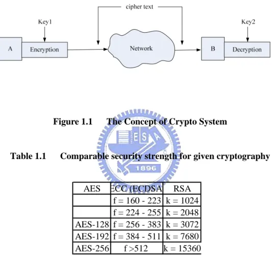
The rapidly growth of internet and wireless communication has led to more requirement on security device to protect the data communication over open channels. If the hacker gets the message without protection, the message is not secret. Cryptography [1] is knowledge to research how to avoid that the hacker gets the real message. The concept of crypto-system illustrated in Fig. 1.1 is used to protect message transmitted over public channel. Every message is encrypted to cipher text with Key1 by Host A before transmitted, and decrypted to plain text with Key2 after received by Host B. According to the Key, two type of crypto-system are classified, such as symmetric-key or private-Key, and asymmetric-key or public-Key crypto-system. The symmetric-key crypto-system uses identical key for encryption and decryption, i.e., Key1 is equal to Key2 or we can get Key2 easily from Key1. DES, 3DES, and AES are symmetric-key algorithms use in symmetric-key crypto-system. The asymmetric-key crypto-system uses different key when encryption and decryption, i.e., Key1 is not equal to Key2. RSA and Elliptic Curve are asymmetric-key algorithms used in symmetric-key crypto-system. All secret-key crypto-systems are based on substitution and transposition. Substitution means mapping from one field to another
and transposition means replacing the element of the message. Because of that the hardware of substitution and transposition is very easy, so secret-key crypto-system is much faster than public-key crypto-system in general. Tab. 1.1 shows each different parameter size with the same level of security strengths compared with given cryptography [2]. The f and k are key length of ECC and RSA.
Figure 1.1 The Concept of Crypto System
Table 1.1 Comparable security strength for given cryptography
AES ECC (ECDSA) RSA f = 160 - 223 k = 1024 f = 224 - 255 k = 2048 AES-128 f = 256 - 383 k = 3072 AES-192 f = 384 - 511 k = 7680 AES-256 f >512 k = 15360
Advanced Encryption Standard (AES) [3] is a symmetric block cipher proposed by National Institute Standard Technology (NIST) of United States. In January, 1997, the NIST announced the start of an initiative to develop a new encryption standard: the AES. The algorithm should be a symmetric-key block cipher, and support block size under 128 bits and key sizes under 128, 192, and 256 bits. The new encryption standard was to become a Federal Information Processing Standard (FIPS), replacing the old Data Encryption Standard (DES) and triple-DES. Then the
first Advanced Encryption Standard Candidate conference (AES1) was held in Ventura, California, August, 1998. Fifteen AES algorithms submitted by members of the cryptographic community around the world were announced in AES1. Five algorithms, MARS, RC6, Rijndael, Serpent, and Twofish, were selected as the finalist in the Second Advanced Encryption Standard Candidate conference (AES2), held in Rome, Italy. Until April, 2000, the Third Advanced Encryption Standard Candidate conference (AES3), held in New York, invited the submitters in finalist to attend and described their algorithm. Finally, NIST selected that Rijndael as the AES algorithm in October, 2000. The AES algorithm has broad applications, including smart cards and cellular phones, WWW servers and automated teller machines (ATMs), and digital video recorders. [4]
1.2 Motivation
In resent years, security issues on communications are more and more significant as the wireless industry explodes. The AES has become an important role in secret-key cryptographic systems. As compared to software implementations, the hardware implementations of the AES algorithm provide more physical security as well as higher speed. AES crypto system needs high throughput. Although the AES hardware for embedded system will limit the performance because of its limited instruction set. So we will provide a hardware AES design for 32 bits embedded system to increase the throughput. And the 『S+Core』 is 32-bit RISC CPU, it established high-efficient development platform with integrated software/hardware tools. The 『S+Core』 CPU compile AES algorithm to several instructions listed in Fig. 1.2. It cost more than 3000 cycle count to encrypt a message. We analyze the instructions in detail. Obviously, it
takes a lot of time to exchange the data and perform finite field computation. We can use hardware to solve this problem. In the design, We make use of 『S+Core』 to finish a cryptographic system, flexibility is the advantage. Because the development of 『S+
Core』 is quite complete, it is convenient in replacing the circuit to make use of development platform to realize the hardware. Because 『S+Core』 has good user’s interface, We devote us to designing the cryptographic systems to work with higher speed, alleviate other burdens.
10% 8%
43% 39%
load & store arith & logic shift_rotate others
Figure 1.2 AES instructions of S+Core
1.3 Organization of this thesis
This thesis is organized as follows. In Chapter 2, we present the AES algorithm. It contains AES basic operations. Chapter 3 shows the proposed architecture of the encryption of AES design. In addition, we also introduce the S+Core Platform. The
verification method and simulation result will be shown in Chapter 4. We make a brief conclusion and future work in the last chapter.
Chapter 2
Algorithm Specification
In this chapter, the Advanced Encryption Standard (AES) algorithm is described.
2.1 Advanced Encryption Standard (AES)
Specification
The input and output of AES specification is described follow in Table 2.1. For the AES algorithm, the length of the input block and the output block is 128 bits, and the different key length will execute different iteration count. For key length 128 bits, 10 iteration is execute, and 12 iteration for 192 bits, 14 iteration for 256 bits.
Table 2.1 AES specification relations
In/Output Block Size Key Length Number of Rounds AES-128 128 bits 128 bits 10
AES-192 128 bits 192 bits 12 AES-256 128 bits 256 bits 14
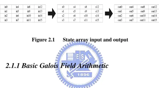
The input – the array of bytes in0, in1, … in15 – is copied into the State array as illustrated in Fig. 2.1. The Cipher or Inverse Cipher operations are then conducted on this State array, after which its final value is copied to the output – the array of bytes
out0, out1, … out15. Roughly, there are 4 kinds of transformation:
1. Non-linear byte substitution, so called SubBytes().
2. Cyclic shift on each row of the State array by different offsets, so called
ShiftRows().
3. Mixing the data within each column of the State array, so called
MixColumns().
4. Adding the round key with the State, so called AddRoundKey().
in0 in4 in8 in12 in1 in5 in9 in13 in2 in6 in10 in14 in3 in7 in11 in15
s0 s4 s8 s12 s1 s5 s9 s13 s2 s6 s10 s14 s3 s7 s11 s15
out0 out4 out8 out12 out1 out5 out9 out13 out2 out6 out10 out14 out3 out7 out11 out15
Figure 2.1 State array input and output
2.1.1 Basic Galois Field Arithmetic
The basic unit for processing in the AES algorithm is byte, and most operation in AES round function is based on GF(28) arithmetic addition and multiplication. The addition in GF(28) is defined as XOR operation, but the multiplication between 8 bit vector will produce a vector longer than 8 bits which in GF(28). Therefore, the finite field multiplication always performs a modular multiplication, that modulo with irreducible polynomial after multiplication. For AES, the irreducible polynomial is
8 4 2
( ) 1
m x =x +x +x + + (2.1) x
2.1.2 Composite Field Arithmetic
We call two pairs
( )
( )
1( )
0 2n , n n i i, i 2 i GF Q y =y +∑
=− q y q ∈GF (2.2) and( )
( )
( )
1( )
0 2n m , m mi i i, i 2n GF P x =x +∑
=− p x p ∈GF (2.3) a composite field [5] if z GF(2n) is constructed from GF(2) by Q(y); z GF((2n
)m) is constructed from GF(2n) by P(x).
Composite fields will be denoted by GF((2n)m), and a composite field GF((2n)m) is isomorphic to the field GF(2k) for k = nm. Additionally, composite fields can be built iteratively from lower order fields. For example, the composite field of GF(28) can be built iteratively from GF(2) using the following irreducible polynomials [6]:
( )
( )
( )
( )
( )
( )
( )
( )
( )
( )
( )
( )
2 2 0 2 2 2 2 1 2 2 2 2 2 2 2 2 2 ... 1 2 2 ... 2 2 ... GF GF P x x x GF GF P x x x GF GF P x x x φ λ ⎧ ⎪ ⇒ = + + ⎪ ⎪ ⇒ = + + ⎨ ⎪ ⎪ ⇒ ⎛ ⎞ = + + ⎪ ⎜ ⎟ ⎝ ⎠ ⎩ (2.4)Whereφ =
{ }
10 2andλ={
1100}
2. Meanwhile, an isomorphic mapping function( )
f x = ×δ x and its inverse need to be applied to map the representation of an element in GF(28) to its composite field and vice versa. The 8×8 binary matrix δ are decided by the field polynomials of GF(28) and its composite fields. Such a matrix can be found by the exhaustive-search-based algorithm in [5]. The δ matrix corresponding to p x( )=x8+x4+x3+ + and the field polynomials in (2.4) can be x 1 found as below:
1 1 0 0 0 0 1 0 0 1 0 0 1 0 1 0 0 1 1 1 1 0 0 1 0 1 1 0 0 0 1 1 0 1 1 1 0 1 0 1 0 0 1 1 0 1 0 1 0 1 1 1 1 0 1 1 0 0 0 0 0 1 0 1 δ ⎡ ⎤ ⎢ ⎥ ⎢ ⎥ ⎢ ⎥ ⎢ ⎥ ⎢ ⎥ = ⎢ ⎥ ⎢ ⎥ ⎢ ⎥ ⎢ ⎥ ⎢ ⎥ ⎢ ⎥ ⎣ ⎦ (2.5)
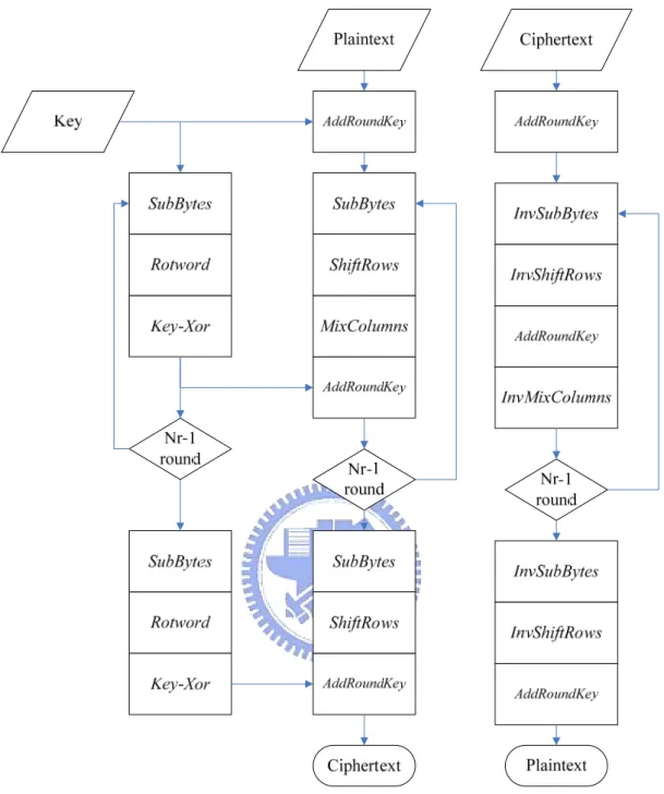
2.2 Encryption and Decryption Procedure
The encryption and decryption procedure are shown in Fig. 2.2. At the beginning of encryption procedure, the plain block is XORed with initial round key, by
AddRoundKey() procedure. After an initial Round Key addition, the State array is
applied to SubBytes(), ShiftRows(), MixColumns(), and AddRoundKey() for 10, 12, or 14 times (depending on the key length), with the final round differing slightly from the first Nr-1 rounds. The State is only applied to SubBytes(), ShiftRows(), and
AddRoundKey(), then the cipher block is outputted. Similar to the encryption
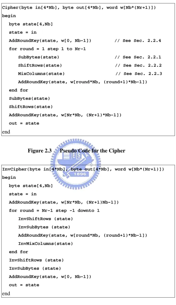
Cipher(byte in[4*Nb], byte out[4*Nb], word w[Nb*(Nr+1)]) begin
byte state[4,Nb] state = in
AddRoundKey(state, w[0, Nb-1]) // See Sec. 2.2.4 for round = 1 step 1 to Nr–1
SubBytes(state) // See Sec. 2.2.1 ShiftRows(state) // See Sec. 2.2.2 MixColumns(state) // See Sec. 2.2.3 AddRoundKey(state, w[round*Nb, (round+1)*Nb-1]) end for SubBytes(state) ShiftRows(state) AddRoundKey(state, w[Nr*Nb, (Nr+1)*Nb-1]) out = state end
Figure 2.3 Pseudo Code for the Cipher
InvCipher(byte in[4*Nb], byte out[4*Nb], word w[Nb*(Nr+1)]) begin
byte state[4,Nb] state = in
AddRoundKey(state, w[Nr*Nb, (Nr+1)Nb-1]) for round = Nr-1 step -1 downto 1
InvShiftRows (state) InvSubBytes (state)
AddRoundKey(state, w[round*Nb, (round+1)*Nb-1]) InvMixColumns(state) end for InvShiftRows (state) InvSubBytes (state) AddRoundKey(state, w[0, Nb-1]) out = state end
The Cipher is described in the pseudo code in Fig. 2.3, and the inverse cipher is described in the pseudo code in Fig. 2.4.
2.2.1 SubBytes() and InvSubBytes() Transformation
The SubBytes() transformation is a non-linear byte substitution that operates independently on each byte of the State using a substitution table (S-box). The S-box is invertible and consists of two transformations:
1. Take the multiplicative inverse in the finite field GF(28), the element {00} is mapped to itself. Tab. 2.2 shows the multiplicative inverse of {xy}16
using Equ. 2.1 as the irreducible polynomial.
2. Apply the following affine transformation (over GF(2)):
'
i i (i+4)mod8 (i+5)mod8 (i+6)mod8 (i+7)mod8 i
b = ⊕b b ⊕b ⊕b ⊕b ⊕c (2.6) for 0≦ i<8, where bi is the ith bit of the byte b, and ci is the ith bit of the
byte c with the value {63}16 or {01100011}2.
In matrix form, the affine transformation element of the S-box can be expressed as:
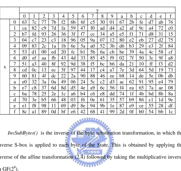
(2.7) Fig. 2.5 illustrates the effect of the SubBytes() transformation on the State. The S-Box used in the SubBytes() transformation is presented in hexadecimal form in Tab.
' 0 0 ' 1 1 ' 2 2 ' 3 3 ' 4 4 ' 5 5 ' 6 6 ' 7 7 1 0 0 0 1 1 1 1 1 1 1 0 0 0 1 1 1 1 1 1 1 0 0 0 1 1 0 1 1 1 1 0 0 0 1 0 1 1 1 1 1 0 0 0 0 0 1 1 1 1 1 0 0 1 0 0 1 1 1 1 1 0 1 0 0 0 1 1 1 1 1 0 b b b b b b b b b b b b b b b b ⎡ ⎤ ⎡ ⎤⎡ ⎤ ⎡ ⎢ ⎥ ⎢ ⎥⎢ ⎥ ⎢ ⎢ ⎥ ⎢ ⎥⎢ ⎥ ⎢ ⎢ ⎥ ⎢ ⎥⎢ ⎥ ⎢ ⎢ ⎥ ⎢ ⎥⎢ ⎥ ⎢ ⎢ ⎥=⎢ ⎥⎢ ⎥+⎢ ⎢ ⎥ ⎢ ⎥⎢ ⎥ ⎢ ⎢ ⎥ ⎢ ⎥⎢ ⎥ ⎢ ⎥ ⎢ ⎥⎢ ⎥ ⎢ ⎥ ⎢ ⎥⎢ ⎥ ⎢ ⎥ ⎢ ⎥⎢ ⎥ ⎢ ⎥ ⎢⎣ ⎥ ⎢ ⎥⎦⎣ ⎦ ⎣ ⎣ ⎦ ⎤ ⎥ ⎥ ⎥ ⎥ ⎥ ⎥ ⎢ ⎥ ⎢ ⎥ ⎢ ⎥ ⎢ ⎥ ⎢ ⎥⎦
2.3. For example, if s1,1 = {53}, then the substitution value would be determined by the
intersection of the row with index ‘5’ and the column with index ‘3’ in Tab. 2.3. This would result in s’1,1 having a value of {ed}.
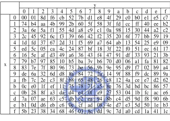
Table 2.2 Multiplicative Inverse table for the byte {xy}16
0 1 2 3 4 5 6 7 8 9 a b c d e f 0 00 01 8d f6 cb 52 7b d1 e8 4f 29 c0 b0 e1 e5 c7 1 74 b4 aa 4b 99 2b 60 5f 58 3f fd cc ff 40 ee b2 2 3a 6e 5a f1 55 4d a8 c9 c1 0a 98 15 30 44 a2 c2 3 2c 45 92 6c f3 39 66 42 f2 35 20 6f 77 bb 59 19 4 1d fd 37 67 2d 31 f5 69 a7 64 ab 13 54 25 e9 09 5 ed 5c 05 ca 4c 24 87 bf 18 3f 22 f0 51 ec 61 17 6 16 5e af d3 49 a6 36 43 f4 47 91 df 33 93 21 3b 7 79 b7 97 85 10 b5 ba 3v b6 70 d0 06 a1 fa 81 82 8 83 7e 7f 80 96 73 be 56 9b 9e 95 d9 f7 02 b9 a4 9 de 6a 32 6d d8 8a 84 72 2a 14 9f 88 f9 dc 89 9a a fb 7c 2e c3 8f b8 65 48 26 c8 12 4a ce e7 d2 62 b 0c e0 1f ef 11 75 78 71 a5 8e 76 3d bd bc 86 57 c 0b 28 8f a3 da d4 e4 0f a9 27 53 04 1b fc ac e6 d 7a 07 ae 63 c5 db e2 ea 94 8b c4 d5 9d f8 90 6b e b1 0d d6 eb c6 0e cf ad 08 4e d7 e3 5d 50 1e b3 f 5b 23 38 34 68 46 03 8c dd 9c 7d a0 cd 1a 41 1c y x
Table 2.3 S-Box, a substitution table for the byte {xy}16 0 1 2 3 4 5 6 7 8 9 a b c d e f 0 63 7c 77 7b f2 6b 6f c5 30 01 67 2b fe d7 ab 76 1 ca 82 c9 7d fa 59 47 f0 ad d4 a2 af 9c a4 72 c0 2 b7 fd 93 26 36 3f f7 cc 34 a5 e5 f1 71 d8 31 15 3 04 c7 23 c3 18 96 05 9a 07 12 80 e2 eb 27 d2 75 4 09 83 2c 1a 1b 6e 5a a0 52 3b d6 b3 29 e3 2f 84 5 53 d1 00 ed 20 fc b1 5b 6a cb be 39 4a 4c 58 cf 6 d0 ef aa fb 43 4d 33 85 45 f9 02 7f 50 3c 9f a8 7 51 a3 40 8f 92 9d 38 f5 bc b6 da 21 10 ff f3 d2 8 cd 0c 13 ec 5f 97 44 17 c4 a7 7e 3d 64 5d 19 73 9 60 81 4f dc 22 2a 90 88 46 ee b8 14 de 5e 0b db a e0 32 3a 0a 49 06 24 5c c2 d3 ac 62 91 95 e4 79 b e7 c8 37 6d 8d d5 4e a9 6c 56 f4 ea 65 7a ae 08 c ba 78 25 2e 1c a6 b4 c6 e8 dd 74 1f 4b bd 8b 8a d 70 3e b5 66 48 03 f6 0e 61 35 57 b9 86 c1 1d 9e e e1 f8 98 11 69 d9 8e 94 9b 1e 87 e9 ce 55 28 df f 8c a1 89 0d bf e6 42 68 41 99 2d 0f b0 54 bb 1c y x
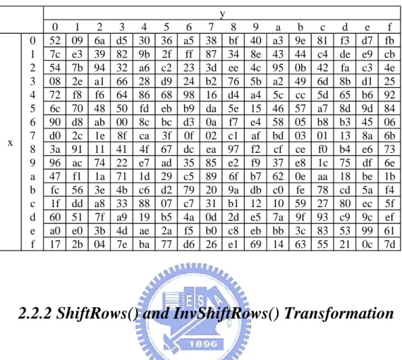
InvSubBytes() is the inverse of the byte substitution transformation, in which the
inverse S-box is applied to each byte of the State. This is obtained by applying the inverse of the affine transformation (2.4) followed by taking the multiplicative inverse in GF(28).
The inverse S-box used in the InvSubBytes() transformation is presented in Tab. 2.4.
Table 2.4 Inverse S-Box, a substitution table for the byte {xy}16 0 1 2 3 4 5 6 7 8 9 a b c d e f 0 52 09 6a d5 30 36 a5 38 bf 40 a3 9e 81 f3 d7 fb 1 7c e3 39 82 9b 2f ff 87 34 8e 43 44 c4 de e9 cb 2 54 7b 94 32 a6 c2 23 3d ee 4c 95 0b 42 fa c3 4e 3 08 2e a1 66 28 d9 24 b2 76 5b a2 49 6d 8b d1 25 4 72 f8 f6 64 86 68 98 16 d4 a4 5c cc 5d 65 b6 92 5 6c 70 48 50 fd eb b9 da 5e 15 46 57 a7 8d 9d 84 6 90 d8 ab 00 8c bc d3 0a f7 e4 58 05 b8 b3 45 06 7 d0 2c 1e 8f ca 3f 0f 02 c1 af bd 03 01 13 8a 6b 8 3a 91 11 41 4f 67 dc ea 97 f2 cf ce f0 b4 e6 73 9 96 ac 74 22 e7 ad 35 85 e2 f9 37 e8 1c 75 df 6e a 47 f1 1a 71 1d 29 c5 89 6f b7 62 0e aa 18 be 1b b fc 56 3e 4b c6 d2 79 20 9a db c0 fe 78 cd 5a f4 c 1f dd a8 33 88 07 c7 31 b1 12 10 59 27 80 ec 5f d 60 51 7f a9 19 b5 4a 0d 2d e5 7a 9f 93 c9 9c ef e a0 e0 3b 4d ae 2a f5 b0 c8 eb bb 3c 83 53 99 61 f 17 2b 04 7e ba 77 d6 26 e1 69 14 63 55 21 0c 7d y x
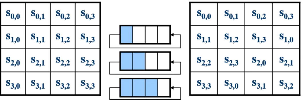
2.2.2 ShiftRows() and InvShiftRows() Transformation
In the ShiftRows() transformation, the bytes in the last three rows of the State are cyclically shifted over different numbers of bytes(offsets). The first row, r = 0, is not shifted.
Specifically, the ShiftRows() transformation proceeds as follows:
'
, ,( ( , )) m od
r c r c shift r N b N b
S = S + for 0< <r 4 and 0≤ <c 4 (2.8) Where the shift value shift(r, Nb) depends on the row number, r, as follows:
( )
1, 4 1shift = shift
( )
2, 4 =2 shift( )
3, 4 =3 (2.9) Fig. 2.6 illustrates the ShiftRows() transformation.s
3,3s
3,2s
3,1s
3,0s
2,3s
2,2s
2,1s
2,0s
1,3s
1,2s
1,1s
1,0s
0,3s
0,2s
0,1s
0,0s
3,3s
3,2s
3,1s
3,0s
2,3s
2,2s
2,1s
2,0s
1,3s
1,2s
1,1s
1,0s
0,3s
0,2s
0,1s
0,0s
3,2s
3,1s
3,0s
3,3s
2,1s
2,0s
2,3s
2,2s
1,0s
1,3s
1,2s
1,1s
0,3s
0,2s
0,1s
0,0s
3,2s
3,1s
3,0s
3,3s
2,1s
2,0s
2,3s
2,2s
1,0s
1,3s
1,2s
1,1s
0,3s
0,2s
0,1s
0,0Figure 2.6 ShiftRows() operates on the row of the State
The InvShiftRows() transformation proceeds as follows:
' '
,( ( , )) m od ,
r c shift r N b N b r c
S + = S for 0< <r 4 and 0≤ <c 4 (2.10) Fig. 2.7 illustrates the InvShiftRows() transformation.
s
3,3s
3,2s
3,1s
3,0s
2,3s
2,2s
2,1s
2,0s
1,3s
1,2s
1,1s
1,0s
0,3s
0,2s
0,1s
0,0s
3,3s
3,2s
3,1s
3,0s
2,3s
2,2s
2,1s
2,0s
1,3s
1,2s
1,1s
1,0s
0,3s
0,2s
0,1s
0,0s
3,0s
3,3s
3,2s
3,1s
2,1s
2,0s
2,3s
2,2s
1,2s
1,1s
1,0s
1,3s
0,3s
0,2s
0,1s
0,0s
3,0s
3,3s
3,2s
3,1s
2,1s
2,0s
2,3s
2,2s
1,2s
1,1s
1,0s
1,3s
0,3s
0,2s
0,1s
0,0Figure 2.7 InvShiftRows() operates on the row of the State
2.2.3 MixColumns() and InvMixColumns()
Transformation
The MixColumns() transformation takes a linear operation on each column – 32-bit word of the State. The linear operation treats the column of the State as a four-degree polynomial over GF(28) and multiplies the column with a fixed polynomial a(x) modulo x4+ . The polynomial a(x) is given by 1
{ }
3{ }
2{ } { }
( ) 03 01 01 02
a x = x + x + x+ (2.11) The polynomial is co-prime tox4+ and therefore is invertible. This operation can 1 also be written as a matrix multiplication. LetS x'
( )
=a x( ) ( )
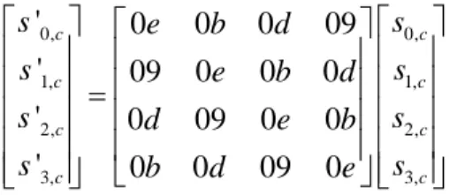
⊗s x0, 0, 1, 1, 2, 2, 3, 3, ' 02 03 01 01 ' 01 02 03 01 ' 01 01 02 03 ' 03 01 01 02 c c c c c c c c s s s s s s s s ⎡ ⎤ ⎡ ⎤⎡ ⎤ ⎢ ⎥ ⎢ ⎥⎢ ⎥ ⎢ ⎥=⎢ ⎥⎢ ⎥ ⎢ ⎥ ⎢ ⎥⎢ ⎥ ⎢ ⎥ ⎢ ⎥⎢ ⎥ ⎢ ⎥ ⎣ ⎦⎢ ⎥ ⎣ ⎦ ⎣ ⎦ (2.12)
Fig. 2.8 describes the effect of the MixColumns() transformation on the State. The elements in column 1 are processed at the same time. After the operation, a(x), the results are generated in column 1.
Figure 2.8 MixColumns() operates on each column of the State
The InvMixColumns() multiplies with the inverse matrix of MixColumns() as follow 0, 0, 1, 1, 2, 2, 3, 3, ' 0 0 0 09 ' 09 0 0 0 ' 0 09 0 0 ' 0 0 09 0 c c c c c c c c s e b d s s e b d s s d e b s s b d e s ⎡ ⎤ ⎡ ⎤⎡ ⎤ ⎢ ⎥ ⎢ ⎥⎢ ⎥ ⎢ ⎥=⎢ ⎥⎢ ⎥ ⎢ ⎥ ⎢ ⎥⎢ ⎥ ⎢ ⎥ ⎢ ⎥⎢ ⎥ ⎢ ⎥ ⎣ ⎦⎢ ⎥ ⎣ ⎦ ⎣ ⎦ (2.13)
2.2.4 AddRoundKey() Transformation
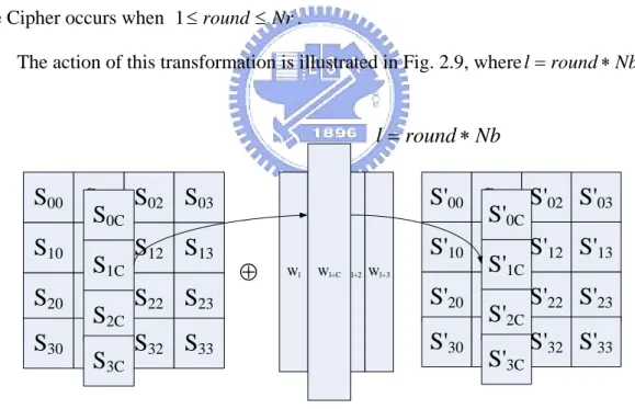
In the AddRoundKey() transformation, a Round Key is added to the State by a simple bitwise XOR operation. Each Round Key consists of Nb words from the key schedule (described in Sec. 2.3). Those Nb words are each added into the columns of the State, such that
' ' ' '
0, 1, 2, 3, 0, 1, 2, 3,
[S c,S c,S c,S c] [= S c,S c,S c,S c]⊕[Wround Nb c∗ + ] for 0≤ <c Nb (2.14) Where [w are the key schedule words described in Sec. 2.3, and round is a value i] in the range0≤round≤Nr. In the Cipher, the initial Round Key addition occurs when round = 0. The application of the AddRoundKey() transformation to the Nr rounds of the Cipher occurs when 1≤round≤Nr.
The action of this transformation is illustrated in Fig. 2.9, wherel=round Nb∗ .
S'
00S
01S'
02S'
03S'
10S
11S'
12S'
13S'
20S
21S'
22S'
23S'
30S
31S'
32S'
33S'
0CS'
1CS'
2CS'
3CS
00S
01S
02S
03S
10S
11S
12S
13S
20S
21S
22S
23S
30S
31S
32S
33S
0CS
1CS
2CS
3C Wl Wl+CWl+2 Wl+3⊕
l =round Nb∗2.3 Key Expansion
The AES algorithm takes the key K, and performs a Key Expansion routine to generate a key schedule. The Key Expansion generates a total of Nb(Nr+1) words: the algorithm requires an initial set of Nb words, and each of the Nr rounds requires Nb words of Key data. The expansion of the input key into the key schedule proceeds according to the pseudo code in Fig. 2.10. As the pseudo code goes, there are different operations to be performed depending on i. Subword() is a operation, consists of 4
SubBytes() operations. RotWord() just performs a cyclic shift, word [a0, a1, a2, a3] will
be shifted as [a1, a2, a3, a0]. The Rcon[i] array, consists of [xi-1, {00}, {00}, {00}],
where the xi-1 is power of x, with irreducible polynomialm x =x +x +x +x+1
( )
8 4 3 in GF(28). The following word, w[i], is derived from the XOR of the preview word, w[i-1], with the word w[i-Nk], which is Nk positions earlier, where Nk means the key length in word. For words in positions that are a multiple of Nk, a transformation, followed by an XOR with the round constant, Rcon[i], is applied to w[i] prior to the XOR with the word w[i-Nk]. This transformation consists of RotWord() andSubWord().
The Key Expansion routine will produce a key array like upper of Fig. 2.11. Whenever the AddRoundKey() routine is invoked, the current index i will increased 4, and the four key after index i are used as input of AddRoundKey(), just as illustrated in lower of Fig. 2.11.
KeyExpansion(byte key[4*Nk], word w[Nb*(Nr+1)], Nk) begin
word temp i = 0
while (i < Nk)
w[i] = word(key[4*i], key[4*i+1], key[4*i+2], key[4*i+3]) i = i+1 end while i = Nk while (i < Nb * (Nr+1)] temp = w[i-1] if (i mod Nk = 0)
temp = SubWord(RotWord(temp)) xor Rcon[i/Nk] else if (Nk > 6 and i mod Nk = 4)
temp = SubWord(temp) end if
w[i] = w[i-Nk] xor temp i = i + 1
end while
end
Figure 2.10 The pseudo Code of the Key Expansion
Figure 2.11 Round Key Select in 192 bit and 256 bit Key Length
k0 k1 k2 k3 k4 k5
Round Key 0 Round Key 1 ...
k0 k1 k2 k3 k4 k5 k6 k7
Round Key 0 Round Key 1 ... k6 k7 k8 k9 k10 k11
Chapter 3
AES Design
In this chapter, we will propose the AES architecture. AES was announced since 2001. Until now, lots of research had shown their AES implementations in hardware or software. In this chapter, we will introduce what is S+Core and how to realize our AES architecture.
This chapter is organized as follows. In section 3.1, consider the system requirement, we modify the AES architecture to match the system request, then new architecture will be given. In section 3.2, we introduce the overview of S+Core, and what is Coprocessor interface (CI). In section 3.3, we present the architecture of the AES.
3.1 AES System Architecture
At the beginning, we use S+Core’s simulator to process the AES encryption procedure, and we find the S+Core’s compiler compile the program inefficient. Because the instruction set of S+Core is limited. So, we can use Coprocessor Interface to solve this problem. The coprocessor is like we plus an accelerator on the system. We will introduce what is S+Core and its Coprocessor Interface in Sec. 3.2. The Coprocessor Interface is the I/O device of our AES design. Our core gets the data from S+Core and starts to encrypt and decrypt the data through the Coprocessor Interface.
Fig. 3.1 shows the block diagram of our AES architecture by Coprocessor Interface. The coprocessor’s general registers receive or transmit data from S+Core only when MTC or LDC instruction is executed, and S+Core gets data from the coprocessor’s general registers when MFC or STC instruction is executed. Take AES-128 for example: First, we give eight MTC or LDC instructions for data and key transmitting from CPU’s general registers or memory unit. We will discuss these instructions in detail in Sec. 3.2.1.And then we start the AES coprocessor when the start signal is assert. Because AES-128 needs 10 cycles to generate the correct cipher, we need Freeze signal to stall the CPU, or the cipher will be wrong. When the Ready signal is assert which means current data is valid, we can transfer the correct 128-bit cipher to coprocessor’s output registers. Finally, we need 4 MFC or STC instructions for transmitting the 128 bits cipher to CPU. Fig. 3.2 shows the waveform of AES-128 encryption.
CLK
rst
START
DATA & Key
Cipher out
Freeze
Ready
Figure 3.2 Waveform of AES-128 encryption
Because of speed consideration, we insert a pipeline register in the core of AES, and Fig. 3.3 shows the block diagram of the core.
Figure 3.3 Pipelined AES core
3.2 Overview of S
+Core Platform
The S+Core™ [12] is Taiwan's first self-defined 32-bit RISC CPU with Sunplus-owned instruction set architecture (ISA). The ISA has 32/16-bit hybrid
instruction mode and parallel conditional execution for high code density, high performance and versatile application. The micro-architecture includes AMBA bus for SoC integration, coprocessor and custom engine interface for function flexibility, and SJTAG for efficient debugging and In-Circuit Emulation (ICE).
The user friendly development environment including S+Core IDE, simulator, optimization GNU C/C++ compiler and GDB enable users to develop the high quality application in fast time.
The most important feature of S+Core is that it has Optional customer-defined coprocessors. That means we can define a new instruction for some dedicated function. Because of that, we can improve the performance of S+Core by customer-defined coprocessors. We will introduce how to use Coprocessor Interface in next section.
3.2.1 Coprocessor Interface (CI)
The S+Core can plug coprocessor 1~3 for some dedicated function; for example, floating pointer device, DSP device. Coprocessor device can plug into S+Core by “Coprocessor Interface”. Up to three Coprocessors may be employed on one design. In this section, we only discuss the coprocessor interface and coprocessor instruction for coprocessor.
S+Core will issue the instruction to coprocessor by CI in first stage. Coprocessor will determine the instruction that belongs to them or not first. And then coprocessor will execute the instruction in it. A coprocessor may contain up to 32 general registers. Each of these registers is up to 32 bits wide. Typically, programs use the general register for loading and storing data on which the coprocessor operates. Data is moved to the coprocessor’s general register from the processor’s general registers with the
MTCz instruction. Data is moved from the coprocessor’s general register to the processor’s general register with the MFCz instruction. Main memory data is loaded into or stored from the coprocessor’s general register with the LDCz and STCz instructions. Fig. 3.4 shows the interaction of S+Core CPU and coprocessor.
All coprocessor instructions share one main opcode encoding. There are three types of coprocessor instruction: coprocessor register transfer instructions, coprocessor data transfer instructions and coprocessor operation instructions. The Sub-OP field distinguishes different coprocessor instructions while CP# specifies the coprocessor number. Coprocessor register transfer instructions are MTC# (move to coprocessor) and MFC# (move from coprocessor). Coprocessor data processing instruction are LDC# (coprocessor load) and STC# (coprocessor store). And Fig. 3.5 shows the coprocessor instructions format.
Coprocessor
Pipeline signal
data
Freeze
Figure 3.4 Coprocessor Interface
mtc/mfc OP rD CrA CP# Sub-OP ldc/stc OP rD CrA CP# Sub-OP cop OP CrD CrA CrB Cop-Code CP# Sub-OP
0 imm10
3.3 Proposed AES Architecture
Fig. 3.6 shows the architecture of our AES core design. The core is composed of three parts, Main function unit, Key Unit, and Control Unit. The Control Unit count the different number of count for different key length. And it generates data ready signal and busy signal to control the AES architecture. The detail components of the Main function Unit will be discussed in Sec. 3.3.1. In our AES design, encryption can run in different key length, such as 128, 192, 256-bit key, and we will discuss how the Key Unit works in Sec. 3.3.2.
Main function Unit Key Unit Control Unit 128 128 Cipher Massage Key 256 128
Figure 3.6 Block diagram of the AES
3.3.1 Efficient implementation of the Function Unit
Because of speed consideration, we process the 128-bit block message in each cycle. The basic architecture unrolls only one full cipher round, and iteratively loops
data through this round until the entire encryption is completed. The basic component is shown in Fig. 3.7.
Figure 3.7 Main function Unit for encryption
SubBytes and InvSubBytes Transformation [4]
The multiplicative inversion in GF(28) involved in the SubBytes is a hardware demanding operation, it takes at least 620 gates to implement by repeat multiplications in GF(28) [7]. However, the gate count can be reduced greatly by using composite field arithmetic. In the SubBytes transformation, using substructure sharing, the isomorphic mapping function can be implemented by 12 XOR gates with 4 XOR gates in the critical path. Meanwhile, the combined inverse isomorphic mapping and the affine transformation can be implemented by 19 XOR gates, and the critical path consists of 4 XOR gates also. In the composite field GF((24)2), an element can be expressed as
h l
s x+ , where s s sh, l∈GF
( )
24 and x is a root of P2(x). Using Extended Euclidean algorithm, the multiplicative inverse of s xh + modulo Psl 2(x) can be computed as in(3.1)
(
)
1(
)
h l h h l
s x+s − = Θ +s x s x+s Θ (3.1)
whereΘ =
(
sh2λ+s sh l +sl2)
−1. The proof of this equation is as follow:( )
2 2P x =x + +x λ is equivalent to finding polynomials A(x) and B(x) satisfying the following equation:
( ) ( )
2( ) ( )
1A x P x +B x S x = (3.2) The B(x) in (3.2) is the inverse of S(x) module P2(x). Such A(x) and B(x) can be
found by using the Extended Euclidean Algorithm for one iteration. First, we need to rewrite P2(x) in the form of
( )
( ) ( )
( )
2
P x =Q x S x +R x (3.3) where Q(x) and R(x) are the quotient and remainder polynomials of dividing P2(x) by
S(x), respectively. By long division, it can be derived that
( )
1(
1)
1 1 h h l h Q x =s x− + +s s s− − (3.4)( )
(
1)
1 1 h l h l R x = + +λ s s s s− − (3.5)Substituting (3.4) and (3.5) into (3.3) and multiplying s to both sides of the h2
equation, it follow that
( )
(
(
)
)
( )
(
)
2 2 2 2 h h h l h h l l s P x = s x+ s +s S x + s λ+s s +s (3.6) Multiplying(
sh2λ s sh l sl2)
1 −Θ = + + to both side of (3.6), we get
( )
(
(
)
)
( )
2 2 1 h h h l s P x s x s s S x Θ = Θ + + + (3.7) Since addition and subtraction are the same in the extended field of GF(2), the first term on the right side of (3.7) can be moved to the left side. Comparing (3.2) and (3.7), it can be observed that( )
(
)
1
h h l
S− x = Θ +s x s +s Θ (3.8) According to (3.1), the multiplicative inversion in GF(28) can be carried out in GF((24)2) by the architecture illustrated in Fig. 3.8.
Figure 3.8 Implementation of the SubBytes Transformation
The SubBytes can be described by
' 1
, ,
i j i j
S =MS− +C (3.9) where M is an 8*8 binary matrix, and C is an 8-bit binary vector with only 4 nonzero bits. The InvSubBytes performs the following operation on each byte of the State
(
)
(
)
1 ' 1 , , i j i j S = M− S +C − (3.10) From (3.10), the InvSubBytes transformation can be implemented according to the block diagram illustrated in Fig. 3.9.MixColumns and InvMixColumns Transformation
Various architectures have been proposed for the implementation of the
MixColumns transformation [6], [8], [9], [10], [11]. Applying substructure sharing both
to the computation of a byte and between the computation of the four bytes in a column of the State, an efficient MixColumns implementation architecture can be derived. Particularly, (2.10) can be rewritten as
' 0, 16 0, 1, 2, 3, 1, ' 1, 16 1, 2, 3, 0, 2, ' 2, 16 2, 3, 0, 1, 3, ' 3, 16 3, 0, 1, 2, 0, {02} ( ) ( ) {02} ( ) ( ) {02} ( ) ( ) {02} ( ) ( ) c c c c c c c c c c c c c c c c c c c c c c c c S S S S S S S S S S S S S S S S S S S S S S S S ⎧ = + + + + ⎪ = + + + + ⎪ ⎨ = + + + + ⎪ ⎪ = + + + + ⎩ (3.11)
According to (3.11), the MixColumns transformation can be implemented by the architecture shown in Fig. 3.10. The function of the block “XTime” is to compute constant multiplication by {02}16. An element of GF(28) can be expressed in
polynomial form as S =s x7 7+s x6 6+s x5 5+s x4 4+s x3 3+s x2 2+s x1 +s0 , where
( )
0, ,...,1 7 2
s s s ∈GF , and x is a root of the field polynomial p(x). Then
{ }
8 7 6 5 4 3 27 6 5 4 3 2 1 0
16
02 S =xS=s x +s x +s x +s x +s x +s x +s x +s x mod p x
( )
=s x6 7+s x5 6+s x4 5+
(
s3+s7)
x4+(
s2+s7)
x3+s x1 2+(
s0+s7) ( )
x+ s7Therefore, the “XTime” block can be implemented by 3 XOR gates with only one XOR gate in the critical path. As illustrated in Fig. 3.5, the total number of XOR gates for computing one column of the State is 108, and the critical path is 3 XOR gates. The
InvMixColumns multiplies the input polynomial by constant polynomial:
( )
1( ) { }
3{ }
2{ } { }
0 0 09 0
d x =c− x = b x + d x + x+ e (3.12) The InvMixColumns is far more complex and occupies larger area. A. Satoh et al. [6] proposed an implantation based idea. This implementation yields logic optimizations since InvMixColumns shares logic resources with MixColumns.
We propose a different method for exploring resource sharing. Recall (2.9) and (3.12). a x
( ) ( ) { }
•d x = 01 . If we multiply both sides of the equation by d(x) weobtain a x
( )
•d2( )
x =d x( )
, where d2( ) { }
x = 04 x2+{ }
05 . Note that two of the coefficients of the d2( )
x are equal to {00}. The MixColumns and InvMixColumnscan be implemented using shared logic resources as shown in Fig. 3.11.
S0 S1 S2 S3
XOR XOR XOR XOR
XOR XOR
XOR XOR
XTime XTime XTime XTime
XOR XOR XOR XOR
S3' S0' S1' S2'
( )
a x
( )
2
d x
Figure 3.11 Implementation of MixColumns and InvMixcolumns
3.3.2 Reconfigurable Key Unit
Fig. 3.12 shows our Key Unit, it is composed of two part, control logic and Key- Generator. The KeyGenerator generate the round key for AES encryption every round. The counter count 10 rounds for 128-bit key, 12 rounds for 192-bit key and 14 rounds for 256-bit key. But we only need 128-bit key in every round, so we use registers to store the round key for next round when 192-bit key and 256-bit key scheduling. The SBox in KeyGenerator is the same as that in Main Function Unit. And the control logic chooses the correct round key for AddRoundKey transformation of Main Function Unit in every round.
Figure 3.12 Block diagram of Key Unit for Encryption
The Key Unit for decryption is different with from that for encryption. At first, we generate all keys for each round and stored in the STACK. When all key we need for decryption is ready, we start to decrypt the cipher. The Fig. 3.13 shows our Key Unit for decryption.
Chapter 4
Simulation and FPGA Verification
AES arithmetic in hardware and design for embedded system are given in this work. This chapter shows the hardware implantation results. The hardware implementation results and design flow are described in Sec. 4.1. The RTL synthesizer uses Synopsys1 Design Compiler for ASIC. The FPGA verification will discuss in Sec. 4.2.
4.1 ASIC Implementation
Fig. 4.1 illustrates the entire ASIC design and testing flow with various CAD (Computer Aided Design) tools. The design is done by pre-layout gate-level simulation but the pre-layout simulation can not calculate the circuit speed precisely. The results for post-layout gate-level simulation will be worse than the results shown in former.
Tab. 4.1 compares our design with other proposed paper. [14] implements the SBox using Look-up-Table. [13] uses composite field arithmetic to implement the SBox. Our design is 2-stage pipelined. The throughput in 128 bit-key length is 1.82Gbps.
Figure 4.1 ASIC design flow
Table 4.1 The AES Core Comparison
Kuo [14] Lai [15] Horng [13] Ours Technology 0.18 0.25 0.18 0.18 Clock rate (MHz) 154 125 125 150 Gate count 173K 80K 67.9K 47.5K Throughput (Gbps) 1.6 1.454 1.6 1.82 Pipeline stage 1 6 1 2 Key Size All 128 All All Function E E/D E/D E
without AES-128 encryption accelerator. Tab. 4.2 shows the time we need to encrypt the first data. We don’t need to spend so much time calculating data as before did.
Table 4.2 The comparison of S+Core with accelerator and not
S+Core (without accelerator) 3329 cycles S+Core (with accelerator) 206 cycles
4.2 FPGA Verification
Figure 4.2 illustrates the FPGA design and testing flow in contrast to the ASIC design flow. Besides the RTL simulation, we also verified our design by using Field Programmable Gate Array (FPGA). Our design is implemented in S+Core, and the operation clock rate is about 33MHz. Tab. 4.3 shows the hardware utilization of our design.
Figure 4.2 FPGA design flow
Table 4.3 The hardware utilization on S+Core
Device S+Core Number of Slice Flip-Flops 20801/93184 (22%)
Number of 4 Input LUT 62400/93184 (66%) clcok rate 33MHz
Chapter 5
Conclusions
First, we have proposed an efficient AES design supported 128, 192, and 256 bits key length. Because of our real time variable KeyGenerator, we don’t need to store all round keys. We only need 10% storage area than others. Second, by implementing the multiplicative inverter in composite field, the area cost can be smaller then that in Look-up-table (LUT). The whole design area can be also reduced by sharing the hardware for encryption and decryption. We also proposed an AES accelerator for 32-bit Embedded Processors. Third, we extend the instruction set of the processor. Because of that, we only need less than 300 cycle count. The processor without accelerator needs over 3000 cycle count to process AES encryption. We speed up 10 times by our design. Besides, from the analysis of various instruction schedules, the 2-stage pipelined architecture is suitable and efficient for most schedules. The total gate count is about 47.5K gates, and maximal throughput is about 1.82Gbps with UMC 0.18 μm process.
Bibliography
[1] W. Stallings, Cryptography and Network Security: Principles and Practice.
Prentice Hall, 2002.
[2] Recommendation on Key Management, NIST Special Publications Std. 800-57, 2005.
[3] J. Daemen and V. Rijmen, AES Proposal: Rijndael, AES Algorithm Submission, September 3, 1999.
[4] X. Zhang, K. K. Parhi, “High-speed VLSI Architectures for the AES algorithm,”
IEEE Trans. On VLSI Systems, vol. 12, no. 9, pp. 957-967, 2004.
[5] C. Paar, “Efficient VLSI architecture for bit-parallel computations in Galois field,” Ph.D. dissertation, Institute for Experimental Mathematics, University of Essen, Essen, Germany, 1994.
[6] A. Satoh, S. Morioka, K. Takano, and S. Munetoh, “A compact Rijndael hardware architecture with S-Box optimization,” in Proc. ASIACRYPT 2001, Gold Coast, Australia, Dec. 2000, pp. 239-254.
[7] M. H. Jing, Y. H. Chen, Y. T. Chang, and C. H. Hsu, “The design of a fast inverse module in AES,” in Proc. Int. Conf. Info-Tech and Info-Net, vol. 3, Beijing, China, Nov. 2001, pp. 298–303.
[8] V. Fischer and M. Drutarovsky, “Two methods of Rijndael implementation in reconfigurable hardware,” in Proc. CHES 2001, Paris, France, May 2001, pp. 77–92.
[9] H. Kuo and I. Verbauwhede, “Architectural optimization for a 1.82 Gbits/sec VLSI implementation of the AES Rijndael algorithm,” in Proc. Cryptographic Hardware and Embedded Systems (CHES) 2001, Paris, France, May 2001, pp.
51–64.
[10] C. C. Lu and S. Y. Tseng, “Integrated design of AES (advanced encryption standard) encrypter and decrypter,” in Proc. IEEE Int. Conf. Application Specific
Systems, Architectures Processors, 2002, pp. 277–285.
[11] X. Zhang and K. K. Parhi, “Implementation approaches for the advanced encryption standard algorithm,” IEEE Circuits Syst. Mag., vol. 2, no. 4, pp. 24–46, 2002.
[12] http://w3.sunplus.com/products/S%2Bcore.asp
[13] C. L. Horng, “An AES cipher chip design using on-the fly key scheduler”, Master Thesis, Dept. Electrical Engineering, National Tsing Hua University, Hsinchu, Taiwan, June 2004.
[14] I. Verbauwhede, P. Schaumont, and H. Kuo, “Design and performance testing of a 2.29Gb/s Rijndael Processor”, IEEE Jour. of Solid-State Circuits, vol. 38, no. 3, March 2003, pp. 569-572, 2003.
[15] Y. K. Lai, L. C. Chang, L. F. Chen, C. C. Chou, and C. W. Chiu, “A novel memory less AES cipher architecture for networking applications”, in Proc.