國 立 交 通 大 學
光 電 工 程 研 究 所
碩士論文
寬能隙半導體微共振腔強耦合作用之研究
Strong Coupling Regime in Wide Bandgap
Semiconductor Microcavity
研
研究
究生
生:
:林
林詳
詳淇
淇
指
指導
導教
教授
授:
:盧
盧廷
廷昌
昌教
教授
授
中
中華
華民
民國
國九
九十
十九
九年
年七
七月
月
寬能隙半導體微共振腔強耦合作用之研究
Strong coupling regime in wide bandgap semiconductor
microcavity
研究生:林詳淇 Student:Shiang-Chi Lin
指導教授:盧廷昌 教授 Advisor:Tien-Chang Lu
國立交通大學電機資訊學院
光電工程研究所
碩 士 論 文
A Thesis
Submitted to Institute of Electro-Optical Engineering
College of Electrical Engineering and Computer Science
National Chiao Tung University
in Partial Fulfillment of the Requirements
for the Degree of
Master
In
Electro-Optical Engineering
July 2010
Hsinchu, Taiwan, Republic of China
中華民國 九十九 年 七 月
寬能隙半導體微共振腔強耦合作用之研究
研究生:林詳淇 指導教授:盧廷昌 教授
國立交通大學光電工程研究所
摘要
半導體微共振腔中在強耦合作用下,光子與激子會混合形成新的準粒子,我 們稱之為極化子(polariton),這樣的粒子具有玻色子的特性,其有效質量很小並 且擁有可調變的色散曲線,因此在研究固態系統的光與物質交互作用中,半導體 微共振腔是一項十分有潛力的研究領域。在此論文中,我們主要著重於在強耦合 作用下寬能隙材料的微共振腔特性研究,分別為混合型氧化鋅微共振腔以及電激 發氮化銦鎵/氮化鎵多量子井微共振腔。 首先,我們研究混合型氧化鋅微共振腔中的高反射率分布式布拉格反射鏡, 其結構為四分之一光學厚度的氮化鋁/氮化鎵薄膜組成。在 20 對氮化鋁/氮化鎵 分布式布拉格反射鏡中,反射率為 97.2%並且停止帶的寬度為 36.6 奈米。另外, 值得注意的是氮化鋁/氮化鎵分布式布拉格反射鏡其反射率中心波長短於 380 奈 米時,反射頻譜會受到氮化鎵嚴重的吸收使得反射率下降。實驗結果可藉由轉換 矩陣計算出在考慮氮化鎵的吸收時反射頻譜的變化。 藉由 1.5 光學厚度的氧化鋅微共振腔,我們在室溫條件下,分別在反射頻譜 和螢光激發頻譜觀察到 68 meV 的拉比分裂值(Rabi-splitting)。然而在實驗結果中, 上極化子由於與激子連續能態的散射,使得在實驗結果中無法清楚地觀察到上極 化子分支。另外,為了對上極化子分支的鑑別度做進一步的討論,我們藉由數值 模擬的方式對不同物理機制條件下的上極化子分支做討論。模擬結果顯示在氧化鎵與氧化鋅的微共振腔中,其主動層厚度分別在 和 0.25的情況下,上極子分 支會變的無法分辨,主要的原因是在於寬能隙材料塊材的微共振腔中,具有較大 的厚度與吸收係數之間乘積。另外,在共振腔與激子兩者模態的能量差距的選擇 上,會偏向於能量差為負值,因為在此條件下,上極化子在較小的波向量會偏向 激子特性,較不會發生激子連續能態散射情形。此外,在寬能隙材料當中,上極 化子分支的鑑別度也會同時受到非均勻性變寬的影響。而在結構的設計上,量子 井結構的微共振腔因為具有較大的激子束縛能以及較小的厚度與吸收係數乘積, 所以在結構的考量上,量子井結構的微共振腔相較於塊材結構會較容易觀察到上 極化子分支。 在此碩論的最後章節中,我們在電激發氮化銦鎵的微共振腔中觀察到強耦合 的情況。藉由變溫電激發頻譜,我們在 280k 的溫度條件下觀察到 6meV 的拉比 分裂值。另外,我們再藉由變角度電激發頻譜的實驗,在 7.4 度的收光角度下觀 察到 7meV 的拉比分裂值。最後我們在改變注入電流的情形下,可以發現隨著注 入電流的增加拉比分裂值也隨著變小,進一步地證明我們在電激發氮化銦鎵微共 振腔元件中觀察到激子與光子的強耦合現象。
Strong coupling regime in wide bandgap semiconductor
microcavity
Student:Shiang-Chi Lin Advisor:Tien-Chang Lu
Institute of Electro-Optical Engineering, National Chiao Tung University
Abstract
In the strong coupling regime, a new quasi-particle termed cavity –polariton
with bosonic characteristics is created from the mixing of photons and excitons. It has
very small effective mass as well as controllable dispersion curves, so that
semiconductor microcavities (MCs) have been widely investigated due to the
enhanced control of light-matter interaction in solid-state systems. In the thesis, we
focus the strong coupling regime between cavity photon and exciton in two wide
bandgap semiconductor microcavities- ZnO based hybrid microcavity and
InGaN/GaN multiple-quantum-well microcavity.
First of all, we investigate high-reflectivity blue-violet distributed Bragg reflectors
(DBRs) based on AlN/GaN quarter-wave layers for the hybrid ZnO-based MCs. The
20-pairs AlN/GaN DBRs achieve peak reflectivity of 97.2% at 440 nm together with a
stopband width of 36.6 nm. Furthermore, the growth of 20-pair AlN/GaN DBR will suffer
significant influence of GaN absorption when the designed DBR wavelength is
shorter than about 380 nm. The experimental reflectivity spectra are modeled by
transfer matrix theory including the effect of GaN absorption to compare the
For bulk ZnO-based microcavity with 1.5λ optical thickness, we observed a
vacuum Rabi-splitting as large as 68 meV at RT based on the angle-resolved
photoluminescence and reflectivity experiments. It is found that the upper polariton
branch (UPB) is blurred in both experiments due to the absorption from scattering
states. Furthermore, we present in detail the possible physical mechanisms leading to
the broadening of UPBs for different designs of MCs by numerical simulations based
on GaAs, GaN and ZnO materials. The calculated results show that the UPBs of the
GaN- and ZnO-based MCs will become indistinct when the thickness of optical cavity
is larger than and 0.25, respectively, mainly attributed to the larger product of the absorption coefficient and the active layer thickness. In wide-bandgap materials, it
would be relatively easier to observe the UPB in the case of negative exciton-photon
detuning due to the exciton-like UPB and lower absorption of scattering states. In
addition, the inhomogeneous broadening would be an important factor causing the
invisible UPB in wide-bandgap semiconductor MCs. We demonstrate that in a
ZnO/ZnMgO multiple-quantum-well MCs, the UPB could be well-defined due to the
large 2D exciton binding energy and the small product of absorption coefficient and
active layer thickness. These results show that the UPBs can be properly defined in
wide-bandgap semiconductor MCs by appropriate design of MC structures.
In the last of the thesis, we report the strong coupling regime in electrically
pumped InGaN-based microcavity. Through the temperature-dependent
temperature of 280 K. Moreover, the angle-resolved EL spectra at 180 K show the
7-meV Rabi-splitting at 7.4, and the splitting value between lower polariton and upper polariton decreases with the increase of current density, which further evidence
Acknowledgements
時間過的很快,從專題生到畢業,在實驗室也待了三年。首先,這期間最 要感謝的就是盧廷昌老師這三年來耐心的教導,從一個連量子觀念都不懂的大專 生,到現在順利的完成學位碩士生,每兩個禮拜充實的 meeting,讓我在這三年 間成長了不少,十分感謝老師這三年來的栽培。當然還有郭浩中老師與王興宗老 師對我的指導,也讓我在研究上的態度有更有想法與堅持。 另外,我要特別感謝的就是把我一手帶大的俊榮學長以及和我一起奮鬥的 永吉。俊榮學長為人熱心,時常搭配著爽朗的笑聲出場,和學弟的相處就像朋友 一樣。在研究上不論是實驗或是觀念都很有條理和見解,真的很慶幸能有這樣的 機會給學長指導。而我的最佳實驗夥伴火星人永吉,在實驗上真的幫了很大的忙, 模擬方面更是一把罩,每次與他的討論總是能獲得建設性的意見。這兩位學長對 我的碩士生研究,真的是不可或缺的貴人啊! 最後還要感謝一起奮鬥的實驗室同仁們,跟我一樣是 GB 系列的阿伯、憨 厚網球一哥信助、吃飯不找不行的板弟,擁有陽光般笑容的 Joseph、超麻吉但腦 子有洞的傻子,超有趣開心果奇葩獸皇,很對 tone 的 Roommate 菲哥、不知長 褲為何物的辣妹依嚀、個性滿點的惟雯、超活潑且語不驚人死不休的嗡嗡、帶點 正經又和李博擊拳的阿翔、緩速靈氣的”絕”高手小胖、擁有水汪汪大眼的哭哭、 話不容易接的怪怪美少女小邱、話不少的彥群、還有新上任的 Microcavity 一哥 思維、表裡不如一的阿國等等…..。這些人為我的碩士班生涯添加了許多回憶和 歡笑,真的很開心能認識你們,也祝福大家在未來的路上都能有很好很好的發展。 半導體雷射實驗室超酷的啦。Content
Abstract (in Chinese)……….………..…………..i
Abstract(in English )………..……….iii
Acknowledgement………...………....vi
Content………...……….…...vii
List of Figures...x
Chaper 1. Introduction………1
1.1 Semiconductor Microcavity………...1
1.2 Strong coupling regime in semiconductor microcavity………4
1.3 Wide bandgap semiconductor microcavity………...7
Chaper 2. Microcavity polaritons………12
2.1 Strong coupling regime and weak coupling regime………...12
2.2 What are microcavity Polaritons……….19
2.2.1 Wannier-Mott exciton………...19
2.2.2 Semiconductor microcavity cavity mode……….21
2.2.3 Microcavity polaritons………..24
2.3 Microcavity polaritons characteristics………26
Chaper 3. Strong
coupling
regime
in
hybrid
ZnO-based
microcavity……….35
3.1.1 Ultra-Violet Distributed Bragg Reflectors………36
3.1.2 Microcavity Structure Design and Quality………...41
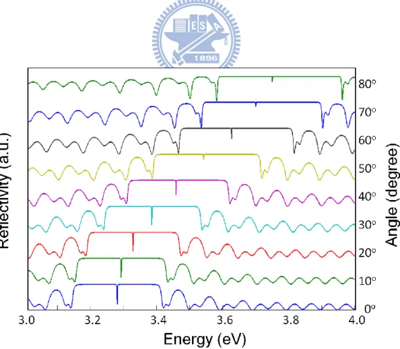
3.2 Angle-Resolved Reflectivity………...42
3.2.1 Principles and Setups………42
3.2.2 Simulation Model………...44
3.2.2.1 Transfer matrix model………...44
3.2.2.2 Oscillator model of strong coupling regime………48
3.2.3 Experimental results of strong coupling regime in ZnO microcavities……….48
3.2.4 Exciton scattering states absorption………..50
3.3 Broadening of upper polariton branch………52
3.3.1 Comparison of UPB broadening between microcavities based on different materials……….53
3.3.1.1 Influenceof the active layer thickness………56
3.3.1.2 Influenceof exciton-cavity detuning………...58
3.3.2 Influence of inhomogeneous broadening………..59
3.3.3 Comparison between QWs-embedded and bulk ZnO-based microcavities……….62
Chaper 4. Strong coupling in InGaN/GaN multi quantum well
vertical cavity surface emitting laser………80
4.2 InGaN/GaN multi quantum well microcavity structure………..84
4.3 Electroluminescence setup and principle………85
4.4 Experimental results………...………85
4.4.1 Temperature-dependent electroluminescence………...85
4.4.2 Angle-resolved electroluminescence………89
4.4.3 Current-dependent electroluminescence………...90
List of Figures
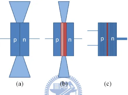
Fig 1.1. Various schemes of lasing with semiconductors………..11
Fig 2.1. The time-dependence of these probabilities……….30
Fig 2.2. Damped Rabi oscillations for diffrent ratio of the damping rate γ………...30
Fig 2.3. Schematic diagram of a free exciton………31
Fig 2.4. Reflection spectra of a typical distributed Bragg mirror………..31
Fig 2.5. Reflectance of an emptyλ/2 microcavity………..…..32
Fig 2.6. Incidence angle θ dependence of the cavity reflectance………..32
Fig 2.7. Cavity dispersion Ecav vs. θ………...………33
Fig 2.8. Anti-crossing of LP and UP energy levels when tuning the cavity energy across the exciton energy by transfer matrix calculation……….33
Fig 2.9. Polariton dispersions and corresponding Hopfield coefficients…………..34
FIg 3.1. Total in-situ reflectance signal at 440 nm for the growth of DBR I……….65
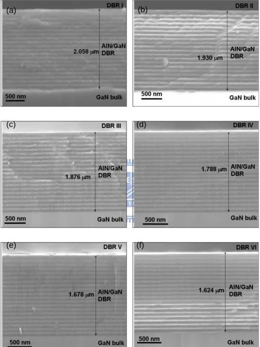
FIg 3.2. The cross-section SEM images of DBRs I-VI……….66
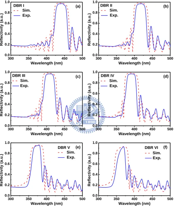
FIg 3.3. Measured and simulated reflectivity spectra of DBR I- VI………..67
FIg 3.4. Measured and calculated maximum reflectivity values and stopband widths of the DBRs I-VI……….68
FIg 3.5. (a) The schematic diagram of the ZnO-based hybrid microcavity. (b) The cross section image of the ZnO microcavity with bottom DBRs observed by SEM……….68
FIg 3.6. Photoluminescence spectrum from the half-cavity ZnO film grown on AlN/AlGaN DBRs………...69
FIg 3.7. Reflectivity spectra of a 30-pair AlN/Al0.23Ga0.77N DBR and a 9-pair SiO2/HfO2 DBR. RT PL spectra from a half cavity………...………..69
FIg 3.8. Reflectivity and PL spectra from the full hybrid microcavity……….70
FIg 3.9. (a) Schematic of experimental setups for measuring reflectance. (b) Practical setup for the angle-resolved reflectivity…………...………70
FIg 3.10. Schematic of the calculation for interface matrix and propagation matrix..71
FIg 3.11. Schematic for multilayer structure for transfer matrix………72
FIg 3.12. Comparison between reflectivity of pure cavity mode and the polariton mode………72
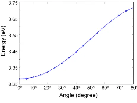
FIg 3.13. Angle-resolved reflectivity spectra ranging from 8° to 40° for detunings of (a) -93 meV and (b)-53meV………73 FIg 3.14. Experimental and theoretical polariton dispersion curves………...73 FIg 3.15. (a) The color map of the measured angle-solved reflectivity spectra. (b) The
color map of the calculated angle-solved reflectivity spectra without taking the resonant exciton into account. (c) The color map of the calculated angle-solved reflectivity spectra with taking the resonant exciton into account……….74 FIg 3.16. Experimental and simulated absorption spectra of a bulk ZnO…………...75 FIg 3.17. (a) Color map of the angular dispersion of measured reflectivity spectra (b)
Color maps of the calculated angle-resolved reflectivity spectra with taking the resonant exciton into account. (c) Simulation of angle-resolved reflectivity spectra for the bulk ZnO MCs after taking the absorption of scattering states into account………...76 FIg 3.18. (a) Schematic diagram of the bulk semiconductor microcavity. (b)
Refractive index profile and the optical-field intensity………...77 FIg 3.19. Color maps of calculated reflectivity spectra as a function of active layer
thickness for GaAs, GaN, and ZnO microcavities………...77 FIg 3.20. Color maps of calculated reflectivity spectra as a function of
exciton-photon detuning for GaAs, GaN, and ZnO MCs………78 FIg 3.21. (a) Calculated reflectivity spectra for the ZnO cavity as varying the
inhomogeneous broadening. (b) Color map of the reflectivity spectra as a function of inhomogeneous broadening………..79 FIg 3.22. Color maps of the calculated angle-resolved reflectivity spectra of 0.5- (a)
MQW ZnO-based MC, (b) bulk ZnO-based MC………79 FIg 4.1. The schematic diagram of completed electrical pumped InGaN-based
microcavity………..92 FIg 4.2. The schematic of low-temperature electroluminescence……….92 FIg 4.3. (a) Series of electroluminescence spectra from polariton emission for
different temperatures between 180K and 300K. (b) Color map of electroluminescence spectra from polariton emission for different temperatures between 180K and 300K. (c) Simulation of
temperature-dependent transmittance spectra from 180K to 300 K (d) Color map of transmittance spectra ranging from 180K to 300K……….…..….93 FIg 4.4. (a)Summarizes the angle-resolved emission spectra measured ranging from
0o to 13o at 180k. (b) Color map of the angle-resolved emission spectra measured ranging from 0o to 13o at 180k. (c) Simulation results for angle-resolved transmittance spectra (d) Color map of simulated angle-resolved transmittance spectra………..……….94 FIg 4.5. Electroluminescence spectra are shown as a function of injection current.95
Chapter 1. Introduction
1.1. Semiconductor microcavitySemiconductors are important materials in light–matter physics thanks to the
radiative recombination of electrons and holes, although not at equilibrium where
their densities are too small to produce a detectable quantity of light even with high
doping. However, it is easy to operate a semiconductor out of equilibrium by applying
an electric voltage to it and generating huge populations of carriers. Indeed, a forward
biased p-n gallium arsenide junction generates strong light in the infrared as reported
in the early 1960s by Hall et al. [1], Nathan et al.[2] and Quist et al.[3]. By increasing
the pumping of the structure to the point where electrons and holes undergo an
inversion of population, the diode reaches the stage where gain overcomes losses
through stimulated emission, and an input signal on the active region is amplified. It
remains to engineer the device so that this input is levied from its output to trigger the
laser oscillations. When the light generated by recombination of electrons and holes
gets to this surface, it is partially reflected back by internal reflection. The reflectivity
is consequently quite low for such lasers, about 30% (the facets can be coated for
better reflection).
For semiconductor laser, these preliminary diode sources were not efficient
lasers as the active region where electron and hole recombine is spread out across the
junction with great losses and requiring significant threshold currents to compensate.
Kroemer [4]: the double heterostructure (DH). It consists of a thin region of
semiconductor with a small energy gap sandwiched between two oppositely doped
semiconductors with a wider bandgap. When forward biased, carriers flow into the
active region and recombine more efficiently because the potential barriers of the
heterostructure confine the carriers to the active region. Practical and soon efficient
operation was achieved and the device became one key element in the computer and
information era, with maybe its most significant impact in the data storage with
optical reading of CD and DVD types of optical disks.
These above-mentioned structures that are now called classical
heterostructures rely on the profile of the energy bands for providing potential traps
for the carriers. Their size varies in the range between a few hundred μm and a few
mm. The idea was pushed forward by reducing further still the area of localization to
the point where size-quantization plays a role, opening the way to quantum
heterostructures, quantum wells, quantum wires and quantum dots. These various
schemes of lasing with semiconductors are sketched in Fig. 1.1.
Until the late 1970s, semiconductor lasers exclusively used the stripe geometry
with cavity lengths longer than 100 μm. However, with the production of high-quality
integrated DBR mirrors, it became possible to rotate the orientation of the emission so
that it emerged normal to the growth-layer planes. The principal advantage of this
surface emission geometry of vertical-cavity surface-emitting Lasers (VCSELs) is the
cleave the wafer into individual lasers with facets, with a large reduction in the cost of
quality control, manufacture and ease of packaging devices. With the introduction of
lattice-matched DBR designs producing 99% to 99.9% intensity reflection
coefficients, the VCSEL dimension can be reduce to about micrometre –sized.
A microcavity is an optical resonator close to, or below the dimension of the
wavelength of light. Micrometre- and submicrometre-sized resonators use two
different approaches to confine light, and the most common microcavity is the planar
microcavity in which two flat mirrors are brought into close proximity so that only a
few wavelengths of light can fit in between them such as VCSEL. Generally, planar
microcavities use two different schemes to confine light. In the first, reflection off a
single interface is used, such as a metallic surface, or total internal reflection at the
boundary between two dielectrics. The second scheme is to use microstructures
periodically patterned on the scale of the resonant optical wavelength, for instance a
planar multilayer Bragg reflector with high reflectivity, or a photonic crystal. Since
confinement by reflection is sometimes required in all three spatial directions,
combinations of these approaches can be used within the same microcavity. To
confine light laterally within these layers, a curved mirror or lens can be incorporated
to focus the light, or they can be patterned into mesas.
Microcavities provide the gain is large enough to make up for the cavity losses.
Because of the short round-trip length, the conditions on the reflectivity of the cavity
of VCSELs), due to their ease of integrable manufacture and their performance. Small
cavity volumes are also advantageous for producing low threshold lasers as the
condition for inversion can be reached by pumping fewer electronic states. On the
other hand the total power produced from a microcavity is in general restricted as
eventually the high power density causes problems of thermal loading, extra
electronic scattering, and saturation. One advantage of a microcavity laser is the
reduced number of optical modes into which spontaneous emission is directed, thus
increasing the probability of spontaneous emission in a particular mode and thus
reducing the lasing threshold.
1.2. Strong coupling regime in planar microcavity
The optical properties of semiconductors and semiconductor structures have
been the subject of intense experimental and theoretical investigation during recent
decades. Consequently, many of the basic physical properties are understood very
well and even used in commercial devices such as semiconductor lasers. When a
quantum well grown in the center of a planar microcavity exhibits a pronounced
exciton resonance and if the widths of the degenerate exciton and pure-cavity lines are
both small enough, one sees two transmission peaks and two reflection dips [5]. This
result of light-matter interaction is called here excitonic normal-mode coupling. In
other words, If the rate of energy exchange between the cavity field and the excitons
becomes much faster than the decay and decoherence rates of both the cavity photons
photon and exciton, which shows the light-matter strong coupling regime. In the
strong coupling regime, it is often related to vacuum-field Rabi splitting of atoms or
to a polariton describing light-propagation in a dielectric medium.
For atoms in a high-finesse cavity one finds a sinusoidal cycling of energy
between the atom and the cavity field, which shows the reversible energy transition
between atom and photon which causing the vacuum-field Rabi splitting. The study
of vacuum-field Rabi splitting has been an exciting subfield of atomic physics.
Thompson et al. demonstrate Rabi splitting with a single atom. This led recently to the
first clear demonstration of the discrete nature of the coherent exchange of energy
between the atom and the quantized electromagnetic field [6]. For such a truly
quantum system the optical properties are changed by the addition of a single photon
or single atom, which is often referred to as the quantum statistical limit. In the
opposite limit of many atoms the system behaves semiclassically, i.e., the light-matter
interaction can be described equally well on the basis of a classical field. Interestingly
enough basically the same structures show very interesting light-matter coupling
effects even under low excitation conditions, where the excitonic resonances
dominate the optical semiconductor properties.
Many of the early experimental studies in quantum well structures were done in
samples having linewidths of several meV. In the late 1980s great progress was made
both in the growth of high-finesse monolithic semiconductor microcavities that
modern quantum well sample can have a narrow linewidth of less than one meV. This
results in very pronounced index changes in the vicinity of the exciton resonance so
that the Fabry-Pérot resonance condition, requiring an integral number of wavelengths
between the two mirrors, can be satisfied at three different frequencies. In strong
coupling regime, the high absorption at line center destroys the transmission at the
central frequency Fabry-Pérot solution. That leaves the two sideband solutions giving
the characteristic strong coupling two peaked transmission spectrum first observed by
Weisbuch et al. in the GaAs/GaAlAs multi quantum well microcavity.
Planar semiconductor MCs in the strong coupling regime have attracted a
good deal of attention owing to their potential to enhance and control the interaction
between the light field with a single resonance of an infinite medium leads to a new
quasi-particle termed cavity–polariton will be created and characterized by bosonic
properties, very small effective mass, as well as controllable dispersion curves. The
control of the aforementioned interaction is expected to lead to the realization of
coherent optical sources such as polariton lasers, which are based on Bose-Einstein
condensation or more strictly non-equilibrium polariton population, due to the
collective interaction of cavity polaritons with photon modes. In contrast to bulk
polaritons, the cavity polaritons have a quasi two-dimensional nature with a finite
energy at zero wave vector, k=0, and is characterized by a very small in-plane
effective mass. These characteristics lead to bosonic effects in MCs that cannot be
polariton lasers. This feature is markedly different from those governing conventional
lasers. Lasing in conventional lasers that we discussed above is predicated upon
population inversion which requires substantial pumping injection. In a microcavity
system involving polaritons, however, the lasing condition uniquely depends only on
the lifetime of the lower polariton ground state. This is expected to lead to extremely
low threshold lasers, even when compared to VCSELs. Through these unique
properties of MC polaritons, the investigation on fundamental physical phenomena
and advanced optoelectronic devices are reported in recent years, such as Bose
Einstein condensates [7, 8], parametric amplifications [9], solid state cavity quantum
electrodynamics [10], and polariton light-emitting diodes [11].
1.3. Wide bandgap semiconductor microcavity
Since the first observation of the vacuum Rabi splitting in GaAs-based
QW-MCs , the strong coupling of light with excitons in semiconductor MCs has
attracted a good deal of interest for fundamental studies of exciton-polariton BEC in
solid state as well as promising applications such as very low threshold vertical cavity
lasers. So far, however, cavity polariton and BEC based on GaAs based MCs are
observable only at very low temperatures because of the slow relaxation of cavity
polariton due to the bottleneck effect. Furthermore, the critical temperature Tc of the
bosonic phase transition for cavity polaritons is not limited by the effective mass but
and by the value of the so-called Rabi splitting proportional to light-matter interaction
strength. This Tc is of the order of a few tens of kelvins in GaAs-based structures and
about 100–200 K in CdTe microcavities. In this respect, GaAs-based polariton LED
[12] and electroluminescence from polariton state in the strong coupling regime [13]
were reported. Yet, these experiments were conducted in the 4 – 10 K temperature
range, and of course with the limitation imposed by low temperatures
It is only natural then wide-bandgap semiconductor based MCs such as GaN and
ZnO came to attract increasing attention for RT polariton devices, such as polariton
lasers, polariton LEDs, and polariton parametric amplifiers. This potential is due to
the large exciton binding energies and oscillator strengths accorded to large bandgap
semiconductors. The GaN technology is now reasonably well developed and it should
come as no surprise that the strong coupling regime in GaN MCs has been observed
by a number of research groups [14-16]. In principle, ZnO is even more attractive as it
has a much larger exciton binding energy of 60 meV [17] as compared to 26 meV for
GaN [18].
Wide bandgap semiconductor optical emitters have experienced tremendous
progress and are now commercially available in the form of blue-violet GaN based
edge emitting laser diodes (LDs) [19] and light emitting diodes (LEDs) which are
sufficiently bright that general lighting applications, dubbed solid state lighting (SSL),
are being pursued vigorously. With high efficiency LEDs for illumination are of
with certain inherent advantages such as resonant cavity LEDs (RCLEDs) and
VCSELs. Owing to significant efforts and ensuing continual advances in GaN
technology, optically [20-23] and electrically [24] pumped GaN-based VCSELs have
been reported at room temperature(RT). The study on GaN-based VCSELs is now
poised to enter a new era wherein the threshold current, optical power emitted,
efficiency and longevity will be drawing more attention. Beyond the standard VCSEL
mentioned above, another type of laser, polariton laser is very attractive owing to its
nearly threshold-less operation through Bose-Einstein condensation using cavity
polaritons whose genesis lies in the interaction between photons and excitons.
Furthermore, ZnO is the other attractive wide band-gap material for the
polariton laser device. ZnO is a II-VI semiconductor with a direct band gap around
3.3 eV, a large exciton binding energy of 60 meV, and extremely high exciton
oscillator strength. In 2002 [25],it as suggested that these properties are ideal in order
to fabricate a new type of coherent light emitter called polariton laser [26] which
would emit light in the blue-UV range. Such laser would have a large technological
interest, since there is, so far, no demonstration of VCSEL working in the UV
frequency range. In parallel, the progress in ZnO technology [27] has made realistic a
polariton laser based on this material. The strong coupling regime has been reported
by several groups, [28-30] which have confirmed that (close of 100 meV) twice that
of the best GaN samples could be achieved. Also some alternative systems to planar
allowed the observation of the strong coupling regime at RT [31].
Therefore, wide bandgap semiconductors such as GaN and ZnO are candidates
for achieving low threshold, ideally threshold-less polariton lasing at RT, owing to
large exciton binding energies and extremely high light-matter interaction constant in
these materials systems. Recently, RT polariton lasing has been observed in a
bulk-GaN MC [32] and multi quantum well (MQW) MC [33]. Since the study of
polariton induced nonlinear phenomena is in its early stages, electrically injected
polariton lasers are awaiting further development. However, the optically pumped
experiments, which have been successful, form the stepping stone for electrical
injection. Low-threshold UV polariton lasers should be of great technological interest
Fig 1.1 Various schemes of lasing with semiconductors (a) the p-n junction where
electron–hole recombination at the interface serve as the active population, (b) the
edge-emitting laser where the active region is confined by a heterostructure and (c)
the VCSEL where localization is pushed to the quantum limit and emission made
Chapter 2. Microcavity polaritons
2.1 Strong coupling regime and weak coupling regime
The quantum treatment between light and atoms is usually developed in terms
of the two-level atom approximation [34]. This approximation is applicable when the
frequency of the light coincides with one of the optical transitions of the atom. The
atom will have many quantum levels, and there will be many possible optical
transitions between them. However, in the two-level atom approximation we only
consider the specific transition that satisfies eq.(2.1-1) and ignore all the other levels.
It is customary to label the lower and upper levels as 1 and 2, respectively.
1 2
E
E
(2.1-1)Our objective is to solve the time-dependent Schrödinger equation for a
two-level atom in the presence of the light. In other words, we must solve:
t Ψ i Ψ H ˆ (2.1-2)
We start by splitting the Hamiltonian into a time-independent partH which ˆ0
describes the atom in the dark, and a perturbation term Vˆ t( )which accounts for the light–atom interaction: ) ( ˆ ) ( ˆ ˆ 0 r V t H H (2.1-3) In the case of a two-level atom, the general solution to the time-dependent
Schrödinger equation reduces to
/ 2 2 / 1 1 21 1 ( ) ( ) ) ( ) ( ) , (r t c t r eiEt c t r eiE t (2.1-4) On substituting this wave function into eq.(2.1-2) with H given by eq.(2.1-3), ˆ0
we obtain: ) ) ( ) ( ( ) ( 0 12 2 11 1 ' 1 t iw e V t c V t c i t c (2.1-5) ) ) ( ) ( ( ) ( 1 21 2 22 ' 2 0 c t V e V t c i t c iwt (2.1-6) Where r d t V j t V i Vij | ˆ( )|
i*ˆ( )j 3 (2.1-7)To proceed further we must consider the explicit form of the perturbationVˆ t( ). In the semi-classical approach, the light–atom interaction is given by the energy shift
of the atomic dipole in the electric field of the light, and we arbitrarily choose the
x-axis as the direction of the polarization so that we can write
) ( 2 cos ) ( ˆ 0 0 iwt iwt e e ex wt ex t V
(2.1-8) where 0is the amplitude of the light wave and the perturbation matrix elements are given by: ij iwt iwt ij e e u V ( ) 2 0 (2.1-9)
where u is the dipole matrix element given by ij
| | 3 *
x d r e i x j uij i j (2.1-10)Since x is an odd parity operator and atomic states have either even or odd
parities, it must be the case that u11= u22 = 0. Moreover, the dipole matrix element represents a measurable quantity and must be real, which implies that u21 =u12, because u21 = u . With these simplifications, eq.(2.1-5) and eq.(2.1-6) reduce to: 12*
) ( ) ( 2 ) ( 2 ) ( ) ( ' 1 0 0 e c t e i t c R iw w t iw w t (2.1-11) ) ( ) ( 2 ) ( 1 ) ( ) ( ' 2 0 0 e c t e i t c R iw w t i w w t (2.1-12)
where we define the Rabi frequency R |u12E0/|
These are the equations that we must solve to understand the behavior of the
atom in the light field. It turns out that there are two distinct types of solution that can
be found, which correspond to the weak-field limit and the strong-field limit
respectively.
We consider the weak-field limit first. The weak-field limit applies to
low-intensity light sources. We assume that the atom is initially in the lower level and
that the lamp is turned on at t = 0. This implies that c1(0) = 1 and c2(0) = 0. With a
low-intensity source, the electric field amplitude will be small and the perturbation
weak. The number of transitions expected is therefore small, and it will always be the
case that c1(t)>>c2(t). In these conditions we can put c1(t) = 1 for all t, so that eq.
(2.1-14) reduces to 0 ) ( ' 1 t c (2.1-13) ) ( ) ( 2 ) ( ( ) ( ) 1 ' 2 0 0 e c t e i t c R iww t i ww t (2.1-14)
According to the rotating wave approximation, we now neglect the second term
in eq.(2.1-14). This is justified by the fact that since δω<<(ω + ω0), the second term is
much smaller than the first. After some manipulation we find:
2 2 2 2 ) 2 / 2 / sin ( ) 2 ( ) ( w wt t c R (2.1-15)
We know in fact that all spectral lines have a finite width Δω. Furthermore, we
are considering the interaction between the atom and a broad-band source such as a
black-body lamp. Such a broad-band source can be specified by the spectral energy
density u(ω), which must satisfy:
u(w)dw Eo2 0 2 1 (2.1-16)We therefore integrate eq.(2.1-16) the spectral line:
/2 2 / 2 0 0 2 2 0 2 12 2 2 0 0 ) 2 / ) ( 2 / ) sin( ( ) 2 ( ) ( w w w w w w u(w) t w w u t c (2.1-17)We now make the approximation that the spectral line is sharp compared to the
broad-band spectrum of the lamp, so that u(ω) does not vary significantly within the
integral. This allows us to replace u(ω) by a constant value u(ω0), and thus to evaluate
the integral. The limiting value for tΔω→∞ is u(ω0)2πt. Hence we finally obtain:
)t u(w u t c 2 122 0 0 2 2( ) (2.1-18)
which is a much more satisfactory result because it implies that the probability that
the atom is in the upper level increases linearly with time.
We now wish to return to the more general case in which the population of the
upper level is significant. It is intuitively obvious that this condition applies when the
light–atom interaction is strong. In other words, we are dealing with the case of strong
electric fields, such as those found in powerful laser beams. In order to find a solution
to eq.(2.1-12) in the strong-field limit we make two simplifications. First, we apply
the previous section. Second, we only consider the case of exact resonance with δω =
0. With these simplifications, eq.(2.1-11) reduces to:
) ( 2 ) ( 2 ' 1 c t i t c R (2.1-19) ) ( 2 ) ( 1 ' 2 c t i t c R (2.1-20)
If the particle is in the lower level at t = 0 so that c1(0) = 1 and c2(0) = 0, the
solution is: ) 2 / cos( ) ( 1 t t c R (2.1-21) ) 2 / sin( ) ( 1 t i t c R (2.1-22)
The probabilities for finding the electron in the upper or lower levels are then
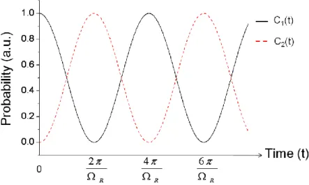
given by: ) 2 / ( cos | ) ( |c1 t 2 2 Rt (2.1-23) )) 2 / ( sin | ) ( |c2 t 2 2 Rt (2.1-24)
The time dependence of these probabilities is shown inFig. 2.1. At t = π/ΩR the
electron is in the upper level, whereas at t = 2π/ΩR it is back in the lower level. The
process then repeats itself with a period equal to 2π/ΩR. The electron thus oscillates
back and forth between the lower and upper levels at a frequency equal to ΩR/2π. This
oscillatory behavior in response to the strong-field is called Rabi oscillation or Rabi
flopping. When the light is not exactly resonant with the transition, it can be shown
that the second line of eq.(2.1-24) is modified to
)) 2 / ( sin | ) ( | 2 2 2 2 2 t t c R R (2.1-25)
Where 2 R2 w2, w being the detuning. This shows that the frequency of the Rabi oscillations increases but their amplitude decreases as the light is tuned
away from resonance.
At low powers, the oscillation period is longer than the radiative lifetime, and
we would expect random spontaneous emission events to destroy the coherence of the
superposition states, and hence curtail the oscillations. We thus have to work at higher
powers to shorten the Rabi flopping period, which can be difficult to achieve in
practice. The damping processes for coherent phenomena such as Rabi flopping are
traditionally characterized by two time constants, T1 and T2. These two types of
damping are sometimes called longitudinal relaxation and transverse relaxation,
respectively. In physical terms, T1 damping is essentially determined by population
decay, whereas T2 damping is related to dephasing processes.
Having considered the processes that cause dephasing in quantum systems, we
can now study the detailed effects of damping on Rabi oscillations. It can be shown
that if the damping rate is γ, the probability that the electron is in the upper level,
namely |c2(t)|2, is given by:
)] 2 3 exp( ) sin ) 4 ( 3 (cos 1 [ ) 2 1 1 ( 2 1 ) ( 2 2 ' 2 1/2 ' 2 t t t t c (2.1-25) Where R
/
4 / 1 2 ' RFig 2.2 shows graphs of |c2(t)|2 from eq.(2.1-25) for three different values of the
damping constant. The dotted line shows the undamped case with γ = 0. The two other
graphs correspond to light damping (γ/ΩR = 0.1) and strong damping (γ/ΩR = 1),
respectively. Let us consider the case of light damping first. The electron performs a
few damped oscillations and then approaches the asymptotic limit with |c1|2 = |c2|2 =
1/2. This asymptotic limit is exactly the behavior we would have expected from the
Einstein analysis of a pure two-level system in the strong-field limit. At high optical
power levels the spontaneous emission rate is negligible and the rates of stimulated
emission and absorption eventually equal out, leading to identical upper and lower
level populations.
Now consider the behavior for strong damping. This is effectively equivalent to
the weak-field limit, because we can always make γ/ΩR large by turning down the
electric field of the light beam. (See eq. (2.1-25)) No oscillations are observed, and
the asymptotic value of |c2|2 for very large damping rates (i.e. ξ>> 1) is given by:
2 2 2 2 4 4 ) ( R t c (2.1-25)
This simple discussion shows how the inclusion of damping allows us to
understand the evolution of the behavior as the electric field strength is increased. At
low fields, we are in the strongly damped regime where there are discrete transitions
and the Einstein analysis is valid. As the field is increased, the ratio of the damping
rate to the Rabi frequency decreases, and we can eventually reach the case where the
2.2 What are microcavity polaritons
2.2.1 Wannier-Mott exciton
The absorption of a photon by interband transition in a semiconductor or
insulator creates an electron in the conduction band and a hole in the valence band.
The oppositely charged particles are created at the same point in space and can attract
each other through their mutual Coulomb interaction. This attractive interaction
increases the probability of the formation of an electron-hole pair, and therefore
increases the optical transition rate. Moreover, if the right condition is satisfied, a
bound electron-hole pair can be formed. This neural bound pair is called and exciton.
In the simplest picture, the exciton may be conceived as a small hydrogenic system
similar to a positronium atom with the electron and hole in a stable orbit around each
other.
Excitons are observed in many crystalline materials. There are two basic
types[35]:
(a) Wannier-Matt excitons, also called free excitons
(b) Frenkel excitons, also called tightly bound excitons
The Wannier-Mott excitons are mainly observed in semiconductors, while the Frenkel
excitons are found in insulator crystals and molecular crystals. In our study, we focus
on the Wannier-Mott excitons having a large radius that encompasses many atoms,
and they are delocalized states that can move freely throughout the crystal; hence the
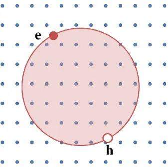
In a free exciton, the average separation of the electrons and holes is much
greater than the atomic spacing, as shown in Fig 2.3. This is effectively the definition
of a Wannier exciton, and it specifies more accurately what is meant by saying that
the free exciton is weekly bound electron-hole pair. Since the electron-hole pair
separation is so large, it is a good approximation to average over the detailed structure
of the atoms in between the electron and hole and to consider the particles to be
moving in a uniform dielectric material. We can then model the free exciton as a
hydrogenic system similar to positronium.
We know from atomic physics that the motion of hydrogenic atoms splits into
the centre of mass motion and the relative motion. The centre of mass motion
describes the kinetic energy of the atom as a whole, while the relative motion
determines the internal structure. The energies of the bound states can be determined
by finding the eigenvalues of the Schrödinger equation for the relative motion. The
main results are well explained by using the Bohr model and this is the procedure we
will adopt here.
In applying the Bohr model to the exciton, we must take account of the fact that
the electron ad hole are moving through a medium with a high dielectric constant
r.Wemust also remember that the reduced mass μwill be given by eq(2.2-1).
* * 1 1 1 h e m m (2.2-1) With these two qualifications, we can then just use the standard results of the
The energy of the nth level relative to the ionization limit is given by 2 2 2 0 1 ) ( n R n R m n E H y r (2.2-2)
where RH is the Rydberg constant of the hydrogen atom (13.6 eV). The quality
H r y m R
R (/ 02) introduced here is the exciton Rydberg constant. The radius of the electron-hole orbit is given by
X H r n n a n a m r 0 2 2 (2.2-3) where aH is the Bohr radius of the hydrogen atom (5.29 × 10⁻¹¹ m) and
H r
X m a
a ( 0 /) is the exciton Bohr radius. Equation (2.2-2) and (2.2-3) show that the ground state with n=1 has the largest binding energy and smallest radius. The
excited states with n>1 at less strongly bound and have a larger radius.
Stable excitons will only be formed if the attractive potential is sufficient to
protect the exciton against collisions with phonons. Since the maximum energy of a
thermally excited phonons at temperature T is about kBT, where kB is Boltzmann‟s
constant, this condition will be satisfied if the exciton binding energy is greater than
kBT. Wannier-Mott excitons have small binding energies due to their large radius, with
typical values of around 10meV. Since kBT is about 25 meV at RT, it is necessary to
direct the interest toward wide band-gap semiconductors for large exciton binding
energy, such as GaN and ZnO. Table 2.1lists the exciton Rydberg constant and Bohr
radius for number of direct gap III-V and II-VI semiconductors.
A typical structure of a semiconductor microcavity consisting of a cavity layer
with mλ/2 (m is integer) sandwiched between two distributed Bragg reflectors
(DBRs). A DBR is made of layers of alternating high and low refraction indices, each
layer with an optical thickness of λ /4. Light reflected from each interface
destructively interfere, creating a stop-band for transmission. Hence the DBR acts as a
high-reflectance mirror when the wavelength of the incident light is within the
stopband. The bottom DBR consists of 2N layers with alternating refraction indices of
n1 and n2, the first layer with refraction index (n1)is next to a cavity layer with
refraction index (nc), while the last layer with refraction index (n2) is next to the
substrate with reflection (ns). For incident light from the cavity side, the maximum
reflectivity is at the center of the stopband
2 2 1 2 2 1 2 2 max ) ( 1 ) ( 1 N s c N s c N n n n n n n n n R
(2.2-4) If the DBR has N + 1 layers with refraction index n1 and N layers with n2, such
as the top DBR, 2 2 1 2 1 1 2 1 2 1 1 2 max ) ( 1 ) ( 1 N t c N t c N n n n n n n n n n n n n R (2.2-5)
where Rmax always increases with N and increases with the refraction index contrast
of the pair. Shown inFig 2.4 are the reflection spectra of a typical DBR.
thickness integer times of λc/2, a cavity resonance is formed atλc, leading to a
sharp increase of the transmission T atλc:
1
4 sin ( /2) ) 1 )( 1 ( 2 2 1 2 2 1 2 1 R R R R R R T (2.2-6) where φ is the cavity round-trip phase shift of a photon at λc.
One characteristic parameter of the cavity quality
2 / 1 2 1 4 / 1 2 1 ) ( 1 ) ( R R R R Q c c (2.2-7) Q is the average number of round trips a photon travels inside the cavity before
it escapes. Fig 2.5 gives an example of the reflection spectrum of a cavity with Q
~4000.
Yet unlike in a metallic cavity, the field penetration depth into the DBRs is
much larger. So effective cavity length is extended in a semiconductor microcavity as:
DBR c eff L L L
(2.2-8) 2 1 2 1 2 n n n n n L c c DBR
(2.2-9) The planar DBR-cavity confines the photon field in the z-direction but not in
plane, incident light from a slant angle µ relative to the z-axis has a resonance at
c/cos . As a result, the cavity has an energy dispersion versus the inplane wavenumber k//: 2 // 2 k k n c E c cav
(2.2-10) where c c n k 2
angle θ and each resonance mode with inplane wavenumber k//: k k n n k c c c c // 1 // when 2 ) sin ( sin tan 2
(2.2-11) In the region k// k, we have:
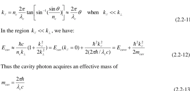
cav cavo c cav c cav m k E c k k E k k k n c E 2 ) / 2 ( 2 ) 0 ( ) 2 1 ( 2 // 2 2 // 2 // 2 2 //
(2.2-12)
Thus the cavity photon acquires an effective mass of
c m c cav 2
(2.2-13) Fig 2.6 gives a numerical example of the angle-tuning, or energy and inplane
wavenumber dispersion of the cavity resonance.
2.2.3. Microcavity polaritons
If the rate of energy exchange between the cavity field and the excitons
becomes much faster than the decay and decoherence rates of both the cavity photons
and the excitons, an excitation in the system is stored in the combined system of
photon and exciton. Thus the elementary excitations of the system are no longer
exciton or photon, but a new type of quasi-particles called the polaritons.
Using the rotating wave approximation, the linear Hamiltonian of the system is
written in the second quantization form as: [36]
) ˆ ˆ ˆ ˆ ( ˆ ˆ ) ( ˆ ˆ ) . ( ˆ ˆ ˆ ˆ // // // // // // // // // // c k k exc k k kk k k k cav I exc opl opl e a e a e e k E a a k k E H H H H c (2.2-14) Here is // ˆka the photon creation operator with inplane wavenumber k// and
longitudinal wavenumberkc kzˆdetermined by the cavity resonance.
// ˆk
exciton creation operators with inplane wavenumber k//.
is the exciton-photondipole interaction given by the exciton optical transition matrix element, and we used
the condition that M is non-zero only between modes with the same k//. The above
Hamiltonian can be diagonalized by the transformation:
// // // // // ˆ ˆ ˆk Xk ek Ck ak p
(2.2-15) // // // // // ˆ ˆ ˆk Ck ek Xk ak q
(2.2-16) And Hˆopl becomes:
// // // // ˆ ( )ˆ ˆ ˆ ) ( ˆ // // k k UP k k LP pol E k p p E k q q H
(2.2-17) The new operators (
// ˆk p
,
// ˆk p ) and ( // ˆk q , // ˆkq ) are the new quasi-particles, or,
eigenmodes, of the system. They are called the lower (LP) and upper polaritons (UP),
corresponding to the lower and upper branches of the eigen energies. A polariton is a
linear superposition of an exciton and a photon with the same inplane wavenumber k//.
Since both excitons and photons are bosons, so are the polaritons. The exciton and
photon fractions in each lower polariton (and vice versa for upper polaritons) are
given by the amplitude squared of Xk//and Ck// which are referred to as the Hopfield
coefficients, they satisfy:
1 2 2 // // k k C X
(2.2-18) Let E(k//)Eexc(k//)Ecav(k//,kc),
// k X and // k C are given by ) 4 ) ( ) ( 1 ( 2 1 2 2 2 // 2 // k E k E Xk
) 4 ) ( ) ( 1 ( 2 1 2 2 2 // // 2 // k E k E Ck
(2.2-20) At ΔE=0, 2 1 2 2 C
X , LP and UP are exactly half photon half exciton, and
the energies of the polaritons, which are the eigenenergies of the Hamiltonian (2.2-17),
are deduced from the diagonalization procedure as:
] ) ( 4 [ 2 1 ) ( // 2 2
,UP exc cav exc cav LP k E E E E
E
(
2.2-21) When the un-coupled exciton and photon are at resonance, Eexc = Ecav, lower andupper polariton energies have the minimum separation Eexc Ecav 2, which is
often called the Rabi splitting in analogy to the atomic cavity Rabi splitting. Due to
the coupling between the exciton and photon modes, the new polariton energies anti-
cross when the cavity energy is tuned across the exciton energy. This is one of the
signatures of 'strong coupling' shown in Fig 2.8. When EexcEcav , the polariton energies reduce to the same as photon and exciton energies due to the very
large detuning between the two modes, and polariton is no longer a useful concept. So
the detuning is assumed to be comparable to or less than the coupling strength in our
discussions unless specified.
2.3 Microcavity polaritons characteristics
The spin number of bosons is number of integer so that the kind of particle does
not necessary to obey the Pauli Exclusion Principle which is much different from the
eingenstate and form the unique physical phenomenon Bose Einstein Condensation.
A polariton is a linear superposition of an exciton and a photon with the same inplane
wavenumber k//, and both excitons and photons are bosons, so the polaritons also have
the bosonic properties.
Compared to other BEC systems, such as atomic gases and excitons, polaritons
have vastly different length, energy and time scales. Beside as an essentially different
system of fundamental interest, polaritons also possess many unique advantages for
BEC research. First of all, the critical temperature of polariton condensation ranges
from a few kelvin to above RT, which is four order of magnitude higher than that of
excitons and eight orders of magnitude higher than that of atoms. It originates from
the critical temperature is inverse proportional to the particle effective mass.
1 / 2 2
2
n
m
T
C
c d (2.3-1)The polariton effective mass is the weighted harmonic mean of the mass of its
exciton and photon components:
cav exc LP m C m X m 2 2 1 (2.3-2) cav exc UP m X m C m 2 2 1 (2.3-3)
where X and C are the exciton and photon fractions given by (2.2-19) and (2.2-20).
mexc is effective exciton mass of its center of mass motion, and mcav is the effective
cavity photon masses given by (2.2-12). Since mcav is much smaller than mexc,
exc cav
LP k m C m
m ( // ~0) / 2 ~104
2 // ~0) /
(k m X
mUP cav
(2.3-5) The very small effective mass of LPs at k// ~0determines the very high critical temperature of phase transitions for the system. At large k// kc// ,
( )
)
(k// E k//
Ecav exc , disperseons of the LP and UP converge to the exciton
and photon dispersions respectively, and LP has an effective mass
exc cav
LP k m C m
m 2 4
// ~0) / ~10
( , Hence the LP's effective mass changes by four order of magnitude from k// ~0 to large k//. Therefore, the polariton effective mass of polaritons is much lighter than atoms and exciton gas due to the mixing with cavity
photons, and most notable for the polariton system is its very light effective mass and
very short time scale which leads to a critical temperature of phase transitions ranging
from 1 Kelvin up to RT.
From the experimental viewpoints, the microcavity polariton is a most
accessible system. There exists a one-to-one correspondence between an internal
polariton in mode k// and an external photon with the same energy and
inplane-wavenumber, propagating at an angle θ from the growth direction. The
polariton is coupled to this photon via its the photonic component with a fixed
coupling rate (2.2-20).The one-to-one correspondence between the internal polariton
mode and the external out-coupled photon mode lends great convenience to
experimental access to the system. The external emitted photon field carries directly
mode, and statistics of the polaritons. It is mainly through the emitted photons that we
study the internal polaritons. Furthermore, polaritons are conveniently excited,
resonantly or non-resonantly, by optical pumping. The excitation density spans the
whole density range of interest. A major enemy against quantum phase transitions in
solids is the unavoidable compositional and structural disorders.
Microcavity system of a given composition has two very useful and unique
adjustable parameters: the active layer thicknessand the cavity-exciton detuning (δ).
For example, the active layer thicknesschanges the exciton-photon coupling strength
QW
N
, where NQW is the number of quantum wells, When Ω is increased to
become comparable with the exciton binding energy, the very strong coupling effect
further reduces exciton Bohr radius in the LP branch and increases the exciton mott
density. The other parameter detuning δ is very conveniently changed due to the taper
of the cavity thickness across each wafer. It tunes the exciton and photon fractions in
the LPs, hence the dispersions, lifetimes, effective mass of the polaritons. This
peculiar parameter has important implications in polaritonic properties, especially for
energy relaxation dynamics of polaritons. A few examples of the polariton dispersion
Fig 2.1 Time dependence of these probabilities for finding the electron in either the
upper or lower level in the strong-field in the absence of damping. The electron
oscillates back and forth between the two levels at the Rabi angular frequency, ΩR.
This phenomenon is either called Rabi flopping or Rabi oscillation.
Fig 2.2 Damped Rabi oscillations for two ratio of the damping rate γ to the Rabi
oscillation frequency ΩR. The dotted curve shows the oscillations when no damping is
Fig 2.3 Schematic diagram of a free exciton which is called Wannier-Mott excitons
Fig 2.5 Reflectance of an empty¸λ/2 microcavity with the Q value of 4000
Fig 2.7 Pure cavity dispersion Ecav vs. θ
Fig 2.8 Anti-crossing of LP and UP energy levels when tuning the cavity energy
across the exciton energy by transfer matrix calculation. X means the exciton mode, C
pure cavity mode, δ cavity-exciton detuning, Ω Rabi-splitting, UPB upper
Fig 2.9 Polariton dispersions and corresponding Hopfield coefficients at (a) δ<0 (b)
δ=0, and (c) δ>0, where the negative detuning shows the obvious polaritonic