國立交通大學
電子工程學系 電子研究所碩士班
碩 士 論 文
基於漢明差值與觸動計數模型之差分能量分析與實作
-以AES晶片為例
Differential Power Analysis on AES Chip with
Hamming-distance and Toggle-count Model
學生:魏廷聿
指導教授:張錫嘉 黃威 教授
基於漢明差值與觸動計數模型之差分能量分析與實作-以
AES晶片為例
Differential Power Analysis on AES Chip with
Hamming-distance and Toggle-count Model
研 究 生:魏廷聿 Student:Ting-Yu Wei
指導教授:張錫嘉 教授 Advisor:Hsie-Chia Chang
黃 威 教授
Wei Hwang
國 立 交 通 大 學
電子工程學系 電子研究所 碩士班
碩 士 論 文
A ThesisSubmitted to Department of Electronics Engineering & Institute Electronics College of Electrical and Computer Engineering
National Chiao Tung University In Partial Fulfillment of the Requirements
for the Degree of Master of Science
In
Electronics Engineering September 2010
Hsinchu, Taiwan, Republic of China
i
漢明差值與觸動計數模型之差分能量分析-以AES晶片
為例
學生:魏廷聿 指導教授:張錫嘉 教授
黃 威 教授
國立交通大學
電子工程學系 電子研究所碩士班
摘 要
在我們當今的日常生活中,人類對於網路和3C產品的使用越來越頻繁,而秘 密資訊便可利用這些產品來做傳遞。為了確保這些資訊安全,加密系統必頇廣泛 的使用在這些產品上。不過,加密系統雖然提供了這些產品的安全性,但沒有人 可以保證這些加密系統是絕對的讓人放心。 差分能量分析攻擊法是一種可以從這些密碼系統中揭露出秘密資訊的威脅, 而差分能量分析攻擊法的執行效率是根據於能量模型的選擇與建立。只要選擇與 建立良好適合的能量模型,攻擊過程將可以省去很多的時間成本。本篇論文將以 AES 90奈米製程的實體晶片為例,實行兩種不同能量模型的攻擊法。漢明差值模 型便是其中一種,它的模型是依據於S-box的輸入端與輸出端的關係。利用漢明 差值的差分能量分析攻擊法可以對於使用查表方式實現S-box的AES晶片成功攻 擊。但根據實驗結果,如果AES晶片的S-box是用composite-field的方式實現的ii
話,針對S-box輸出輸入端作攻擊的這種漢明差值便無法使我們成功攻擊這顆晶 片。因此,我們必頇找出替代的能量模型,針對S-box來攻擊,並且完成破解晶 片的研究。而我們想使用這能量模型,觸動計數模型,來取代漢明差值模型。它 統計了當S-box正在運行時所產生logic gate的所有轉換。
iii
Differential Power Analysis on AES Chip with
Hamming-distance and Toggle-count Model
Student:Ting-Yu Wei Advisor:Dr. Hsie-Chia Chang
Dr. Wei Hwang
Department of Electronics Engineering
Institute of Electronics
National Chiao Tung University
Abstract
In our daily life, the applications of internet and 3C products are used more frequently. The secret information is transported through these applications. In order to ensure the information security, some cryptographic systems have been adopted widely. Cryptographic system indeed can provide the security. However, no one can ensure that cryptographic system can absolutely protect the information security.
Differential power analysis (DPA) attack is one of the threats [11] that could reveal the secret in the cryptographic system. The main efficiency of DPA attack is depended on the power model of attack method. Getting suitable power model, it could cost less time to finish the attack. This thesis describes differential power analysis attack with two kinds of power models on an Advanced Encryption Standard (AES) chip fabricated in 90nm CMOS. One kind of power model is Hamming-Distance model that calculates the relationship between input and output of S-box. The differential power analysis attack with the Hamming-distance model can
iv
attack the AES chip based on look-up-table S-box successfully. But according to the experiment results, it cannot attack the AES chip based on composite-field S-box successfully. So, other power model should substitute for the Hamming-distance model to complete the DPA attack. The substitute power model is toggle-count model that get the statistics of the switching activities from the logic gates during the S-Box process.
v
誌 謝
感謝交通大學,讓我在碩士生涯加上大學生涯收穫許多,在許多師長的提攜 以及同學朋友的鼓勵幫助下,讓我的研究路程充滿驚奇與收穫。首先我要感謝我 指導教授張錫嘉老師,年輕有衝勁且親切的老師不僅能和我們討論到研究內容, 對學生有著無限的包容與體諒,非常的關心學生,不只在學業研究方面,也很看 重每個學生的身心理狀況,甚至能和我們聊一些有趣的事。老師不只在研究上, 或在待人處事上,都是讓我覺得自己要向老師看齊的。另外我也要感謝我的共同 指導教授黃威老師,因為黃老師的指導建議, 改善了很多論文上的缺點,使得我 的論文更完整。 再來要感謝Star group 的全部成員,尤其要感謝林建青學長和劉柏均學長, 透過他們的指導,讓我在專業領域中獲益良多。而在遇到瓶頸問題時,學長也教 了我解決問題的方法,幫助我很順利完成各項研究進度。當然也感謝實驗室的每 位學長同學和學弟妹們,讓我度過了一個充實又開心的研究生涯。Si2實驗室的 同學們,點子和建螢,沒有你們,我也無法完成這次的研究。當然曾經幫助過我 的人,我一定不會忘記你們曾經對我的恩情。 另外要感謝這段日子陪伴我的夥伴,勇志,其衡,耀琳,Qmo,大嘴,永裕, 振揚,高手,歐卡西,玉婷,渠,土豪,傻蔡,尾力,俗氣翔,陳廷,布丁,八 千姊,Jens Floss,還有教會的朋友們,謝謝你們的陪伴、鼓勵與嘴砲,一起運 動歡笑流汗喝酒等,讓我的研究生涯不至於太苦悶,有知識也有知性。 我也要感謝曾經是不斷的在背後支持我的琬庭,妳是對我那麼的無私,那麼 的有耐心,時時相伴而給我力量,真的很謝謝妳。最後,僅將此論文獻給疼愛我 的父母與姊姊姊夫,謝謝你們的愛與讓我能夠無憂無慮的學習,每當我要倒下的 時候,都還能倚靠著你們,真的非常非常的謝謝你們,我感到非常的幸運與幸福。vi
Differential Power Analysis Attacks on AES Chip
with Hamming-distance and Toggle-count Model
Student:Ting-Yu Wei
Advisor:Hsie-Chia Chang, Wei Hwang
Department of Electronics Engineering
National Chiao Tung University
vii
Content
摘 要... i Abstract ... iii 誌 謝... v Content ... vii List of Figures ... ix 1 Introduction ... 1 1.1 Motivation ... 1 1.2 Thesis Organization ... 22 Differential Power Analysis Attack (DPA) ... 3
2.1 General Introduction ... 3
2.2 The Strategy of the DPA Attack ... 4
2.3 Statistical Analysis ... 11
3 Introduction of Advanced Encryption Standard (AES) ... 14
3.1 General Introduction ... 14
3.2 AES Algorithm Steps ... 17
3.2.1 SubBytes Transformation... 17
3.2.2 ShiftRows Transformation ... 19
3.2.3 MixColumns Tranformation ... 20
3.2.4 AddRoundKeys Transformation ... 21
3.2.5 KeyExpansion ... 22
4 Practical Implementation for DPA Attack on AES ... 26
viii
4.2 Practical Implementation ... 30
4.3 Power Model ... 34
4.3.1 Hamming-distance Power Model ... 35
4.3.2 Toggle-count Power Model ... 36
4.4 Result ... 40
4.5 Inference and Comparison ... 42
5 Conclusion and Future Work ... 43
5.1 Conclusion ... 43
5.2 Future Work ... 44
ix
List of Figures
Figure 2.1: Inverter. ... 4
Figure 2.2: Step1: Prepare the plaintexts or ciphertexts. ... 5
Figure 2.3: Step 2: Measure the power trace corresponding to the data blocks. ... 6
Figure 2.4: Step 3: Calculate the hypothetical intermediate value. ... 7
Figure 2.5: Step 4: Generate hypothetical power consumption values. ... 8
Figure 2.6: Step 5: Compare the hypothetical power consumption values with the power traces. ... 10
Figure 2.7: The five steps of DPA attacks. ... 11
Figure 3.1: AES algorithm flow. ... 15
Figure 3.2: Key, block, round combination for AES-128,192,256. ... 15
Figure 3.3: The transformation of the input → state array 4x4. ... 17
Figure 3.4: The two steps of SubBytes transformation... 17
Figure 3.5: SubBytes transformation. ... 18
Figure 3.6: The look-up-table of S-Box. ... 19
Figure 3.7: Shiftrows transformation. ... 20
Figure 3.8: MixColumns transformation. ... 20
Figure 3.9: Addroundkeys transformation. ... 21
Figure 3.10: The whole roundkeys of the keyexpansion for AES-128. ... 25
Figure 4.1: The whole experiment environment. ... 27
Figure 4.2: Logic analyzer with pattern generator. ... 28
x
Figure 4.4: The AES chip ... 30
Figure 4.5: The ASIC board placing. ... 31
Figure 4.6: The CSV file. ... 32
Figure 4.7: Divide the power traces. ... 33
Figure 4.8: Align the power traces. ... 34
Figure 4.9: Hamming-distance power model. ... 35
Figure 4.10: The toggle count. ... 36
Figure 4.11: Glitches happened during the executing process. ... 37
Figure 4.12: Toggle-count power model for the input 0. ... 38
Figure 4.13: To build the toggle-count model by Perl. ... 39
Figure 4.14: The numbers of toggle-count for 256 keys. ... 39
Figure 4.15: Choose a toggle-count number from 256 choices... 40
Figure 4.16: The result of the Hamming-distance power model. ... 41
Figure 4.17: The result of the toggle-count power model. ... 41
1
Chapter 1
Introduction
1.1 Motivation
In recent decades, information technology grows extremely in our daily life. And the information may be transported through ATM cards, mobile phone SIM cards, etc. The smart card could be a representative of tamper-resistant device. Nowadays, we have to pay more attention to the security of the information. The chip embedded on the smart card is given with storing secret information and computing cryptographic algorithm. Therefore, the smart card can be applied for authenticating, encryption and decryption, signing for digital signature, even combining with E-commerce. So, the importance due to the security of the information cannot be neglected.
However, when executing the algorithm in the smart card, there are still threats needed to be considered. While encryption and decryption, the smart card processor would be related with secret data or message. Because of the CMOS characteristics, the executing processor leak some information related to the secret data, called the side-channel information. By collecting and analyzing the side-channel information, attackers could use some methods to discover the secret data. According to the
2
side-channel information, there are three different ways to attack the cryptographic system, called power analysis attack, timing attack, and electromagnetic attack. These attacks are generally called physical attack.
In smart card, one of the cryptographic systems is symmetric block cipher. In 1977, the Data Encryption Standard (DES) is adopted by National Institute of Standards and Technology (NIST) as Federal Standard. DES was reviewed approximately every five years to check if it is still adequate as standard. Its last renewal was in January 1999. By that time, the Advanced Encryption Standard (AES) had already been developed. In this thesis, we always focus on power analysis attack on AES. To collect the power consumption is not too hard for attackers. The power analysis attack is really great threat to the cryptographic system on the smart card.
1.2 Thesis Organization
This thesis consists of 5 chapters. The methods related to power analysis attack including differential power analysis (DPA), and correlation are presented in chapter 2. In chapter 3, the concept of the algorithm of AES will be introduced. In chapter 4, we talk about the implementation corresponding to the device in the environment, and the corresponding practical attack flows, the power models and experiment results. Finally, we make the conclusion in chapter 5.
3
Chapter 2
Differential Power Analysis Attack
2.1 General Introduction
Differential power analysis (DPA) attacks are most popular type of power analysis attack because DPA attacks is one of the most efficient attacks. It doesn’t need lots of detailed information from the attacked target. So, what information does a DPA attack need for an attacker? In the beginning, an attacker should measure the power consumption from the attacked target as precisely as possible. The goal of DPA attacks is to get the secret keys from the cryptography device based on lots of power consumption information. Second, the attacker must figure out what the cryptography algorithm inside the target. Nowadays, it is not difficult to get the idea that what kind of algorithm is computed inside the specific target. Third, the attacker requires the plaintexts or ciphertexts. The main idea of DPA attacks of the attacker is to make a large number of measurements, and then divide them with some methods into different sets. Statistical calculations are used to verify the dividing-methods. If the method is right, the attacker can see some notices in the statistics. The point means that DPA attacks analyze how the power consumption at the fixed time depends on the
4
processed data.
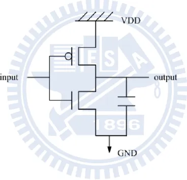
In this age, Complementary metal oxide semiconductor (CMOS) technology constructs almost all digital circuit. Attackers have to know the power consumption characteristics of CMOS technology. Power consumptions can be measured at the VDD or GND pin if a CMOS gate changes its state. The more circuits change the state, the more power is dissipated, and the more information leaked from the device [3].
Figure 2.1: Inverter.
2.2 The Strategy of the DPA Attack
Instead of the first article on DPA attacks in 1999 [1], the so-called difference-of-means method, the correlation coefficient has been considered to analyze our data and the leakage information. The following is the general strategy
5
that how to attack the cryptography devices successfully [4].
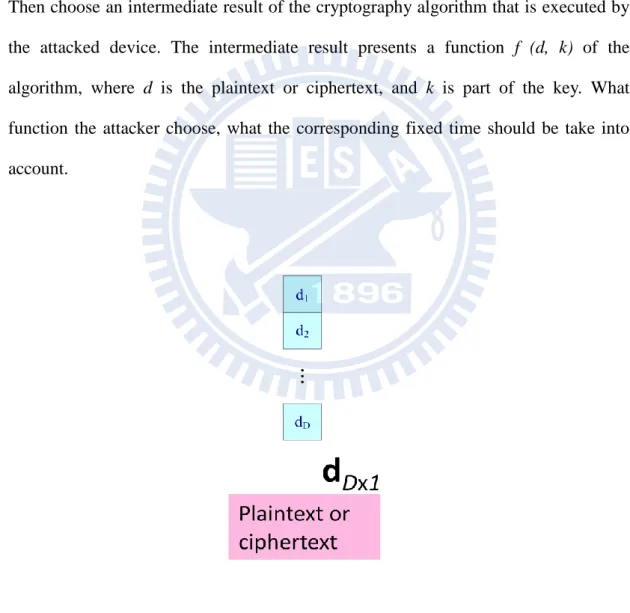
Step 1:
Prepare plaintexts or ciphertexts and choose an intermediate result at a
fixed time of the algorithm.
The first step of a DPA attack for attacks is to prepare a large number of plaintexts or ciphertexts. The plaintexts or ciphertexts are known random data values. Then choose an intermediate result of the cryptography algorithm that is executed by the attacked device. The intermediate result presents a function f (d, k) of the algorithm, where d is the plaintext or ciphertext, and k is part of the key. What function the attacker choose, what the corresponding fixed time should be take into account.
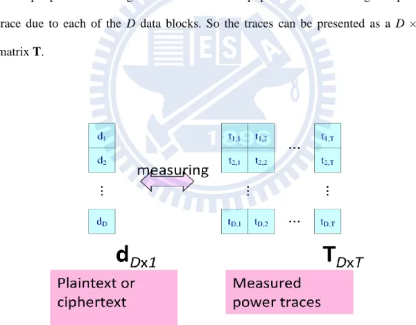
6 Step 2:
Measure the power consumption.
The second step of DPA attack for an attacker is to get the power consumption trace of the cryptography device executing the encryption or decryption with D random data blocks. The corresponding data value d that is involved in the intermediate result need to be confirmed. We present the data values in this way, d = (d1, …, dD)’, where di is the data value in the ith executing run. The attacker measures
each power trace during each of the runs. Corresponding to the data blocks di, we
write the power trace as ti = (ti, 1, …, ti, T), where T is the length of time, or the number
of sample points according to the measurement equipment. The attacker gets a power trace due to each of the D data blocks. So the traces can be presented as a D × T matrix T.
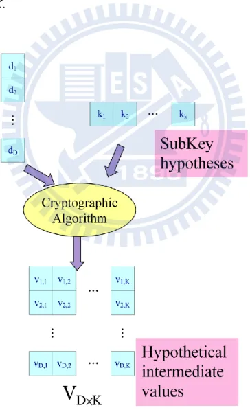
7 Step 3:
Calculate the hypothetical intermediate value.
Here, we list all possible choice of keys as vector k = (k1, …, kK), where K
means the total numbers of possible choices for k, and we refer to k as key hypotheses. After preparing the data blocks d and the key hypotheses k well, the attacker can calculate the hypothetical intermediate values through f (d, k) in the cryptographic algorithm with D data blocks and K key hypotheses. This calculation results in a matrix V, which size is D × K. The elements in V denote as vi,j = f (di, ki), where i = 1
to D and j = 1 to K.
8
From the matrix V, it is not hard to realize that each column of V has been calculated based on the same key hypothesis. Because that k includes all possible key hypotheses, the correct key used in the cryptographic device is the one of the element in k. The key used in the cryptographic device is written as kck. Hence, kck is what the
attacker is eager for.
Step 4:
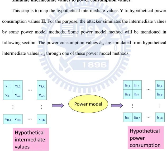
Simulate intermediate values to power consumption values.
This step is to map the hypothetical intermediate values V to hypothetical power consumption values H. For the purpose, the attacker simulates the intermediate values by some power model methods. Some power model method will be mentioned in following section. The power consumption values hi,j are simulated from hypothetical
intermediate values vi,j through one of these power model methods.
9
The efficiency of the DPA attack strongly depends on the power model simulation. And the quality of the simulation depends on the knowledge of the attacker from the attacked device. The attacker should choose a power model that can make the simulation more closely to the actual power consumption characteristics of the attacked device. The more closely the simulation is, the more effective the DPA attack is.
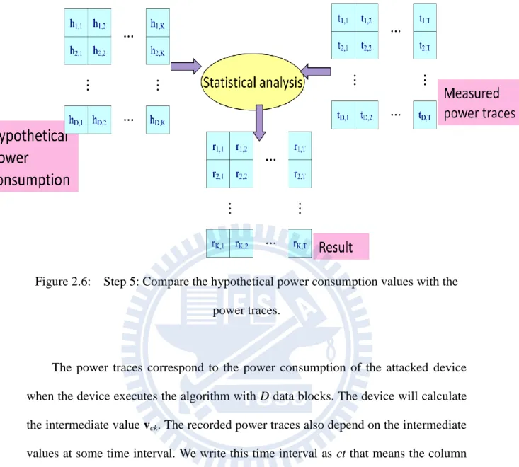
Step 5:
Compare the hypothetical power consumption values with the power traces.
Reviewing the above four steps, we have the V, the hypothetical intermediate value matrix, H, the hypothetical power consumption matrix, and T, the power trace matrix. In this step, the attacker compares the each column hi of H with each column
ti of T. this means the hypothetical power consumption values of each key hypothesis
are compared with the recorded power traces at every time interval. After comparing
H and T, the result is a matrix R of size K × T, where the element ri,j is the result from
the columns hi and tj. This comparison is based on some statistical analysis mentioned
10
Figure 2.6: Step 5: Compare the hypothetical power consumption values with the power traces.
The power traces correspond to the power consumption of the attacked device when the device executes the algorithm with D data blocks. The device will calculate the intermediate value vck. The recorded power traces also depend on the intermediate
values at some time interval. We write this time interval as ct that means the column
tct is the power consumption corresponding to the vck. And the hypothetical power
consumption values hck are simulated based on vck. Therefore, the columns hck and tct
are related strongly, and the result from these two columns hck and tct is the highest
value in R, written as rck,ct. Other values are not as high as rck,ct because the other
11
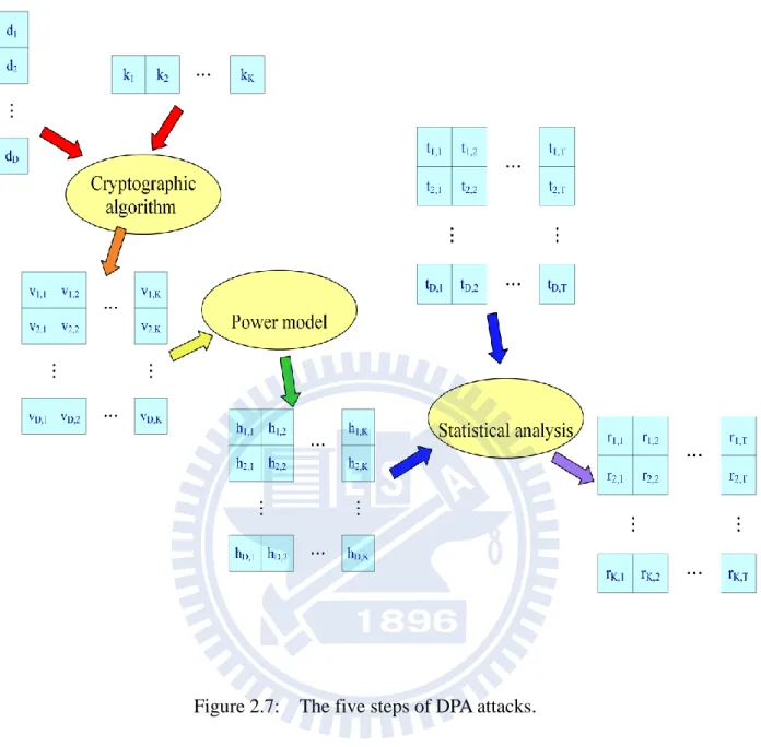
Figure 2.7: The five steps of DPA attacks.
2.3 Statistical Analysis
In this thesis, the correlation coefficient has been considered to perform the DPA attack [15]. The correlation coefficient is to represent the relationships between data, i.e. how strongly the columns of H and T are related.
12
deviation in statistical analysis. X and Y is random variable. The square of the standard deviation is called variance.
11
n i iE X
x
x
n
(2.1) 2 2 2 11
(
)
((
(
)) )
(
)
1
n i iVar X
E X
E X
x
x
n
(2.2)The is an estimate sign from the experiments. We can express the linear relationship between two points of a trace based on the covariance or the correlation. The covariance is given as
( , )
((
( )) (
( )))
Cov X Y
E X
E X
Y
E Y
(2.3)(
)
( )
( )
E XY
E X
E Y
(2.4) The covariance formula is the average of the product of the deviation for the random variable X and Y. It shows that the covariance is related to the concept of the statistical dependence. If X and Y are statistically independent, . So, . The concept is reversible. Therefore, if , X and Y are independent. The covariance should be estimated from the experiments, so the estimator c is given as 11
(
) (
)
1
n i i ic
x
x
y
y
n
(2.5)The correlation coefficient [22] is a more common way to find a linear relationship between two values. And it also should be estimated. It is always between -1 and 1.
13
( , )
( , )
( )
( )
Cov X Y
X Y
Var X
Var Y
(2.6) 1 2 2 1 1
(
) (
)
(
)
(
)
n i i i n n i i i ix
x
y
y
x
x
y
y
(2.7)
In DPA attack, the correlation coefficient is used to determine the linear relationship between the columns hi and tj where I =1, …, K and j=1, …, T. We
estimate the value ri,j according to the D element of the columns hi and tj, where the
I and j are the mean values of the columns hi and tj [10].
, , 1 , 2 2 , , 1 1
(
) (
)
(
)
(
)
D d i i d j j d i j D D d i i d j j d dh
h
t
t
r
h
h
t
t
(2.8)14
Chapter 3
Introduction of Advanced
Encryption Standard (AES)
3.1 General Introduction
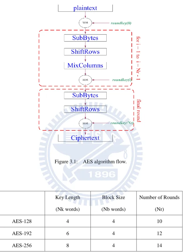
In 1997, NIST began the process of choosing the replacement for DES. After the AES Candidate Conference in April 2000, AES [2] was adopted as a standard on November 26, 2001, and it was published as Federal Information Processing Standards (FIPS) 197 in the Federal Register on December 4, 2001.
The AES has block length 128, and there are three allowable key lengths, namely 128 bits, 192 bits, and 256 bits. AES is an iterated cipher. The number of rounds donated by Nr depends on the key length. Nr = 10 if the key length is 128 bits. Nr = 12 if the key length is 192 bits. And Nr = 14 if the key length is 256 bits. The differences among these three types of key length are small. Therefore, in this thesis, we make AES-128 as our example.
15
Figure 3.1: AES algorithm flow.
Key Length (Nk words) Block Size (Nb words) Number of Rounds (Nr) AES-128 4 4 10 AES-192 6 4 12 AES-256 8 4 14
16
The AES is a symmetric block cipher. Its algorithm proceeds through 4-stage transformation, SubBytes, ShiftRows, MixColumns, and AddRoundKeys. It encrypts as follows[19] [20]:
In AES-128 algorithm, the plaintext consists of 16 bytes, donated x0, ..., x15. State
is represented as a four by four array of bytes. State is defined to consist of the 16 bytes of the plaintext xi.
Encryption Cipher (State, CipherKey) {
Key Expansion( CipherKey, RoundKey ); AddRoundKey( State, RoundKey[0] ); for(i =1; i < Nr; i++)
{
SubBytes(State); ShiftRows(State); MixColumns(State);
AddRoundKeys ( State, RoundKey[i] ); }
SubBytes(State); ShiftRows(State);
AddRoundKey ( State, RoundKey[Nr] ); }
17
Figure 3.3: The transformation of the input → state array 4x4.
3.2 AES Algorithm Steps
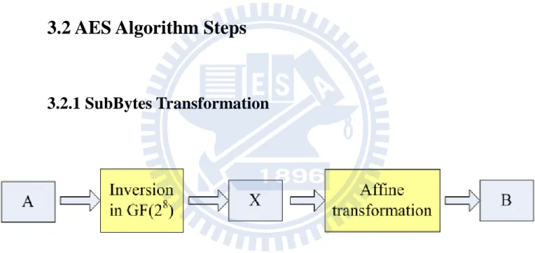
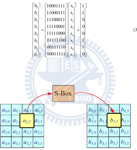
3.2.1 SubBytes Transformation
Figure 3.4: The two steps of SubBytes transformation.
The SubBytes transformation is a non-linear byte substitution that operates independently on each byte of the state using a substitution table (S-box). This S-Box, which is invertible, is constructed by composing two transformations:
1. Take the multiplicative inverse X(x7…x0) for A(a7…a0) in the finite field GF(28).
18
2. Apply the following affine transformation over GF(2). X(x7…x0) → B(b7…b0).
For i = 0 to 7, bi ← xi + xi+4 + xi+5 + xi+6 + xi+7 + ci mod, ci is the ithbit of a byte C
with the value {63}. The affine transformation element of the S-box can be expressed as: 0 0 1 1 2 2 3 3 4 4 5 5 6 6 7 7 10001111 1 11000111 1 11100011 0 11110001 0 11111000 0 01111100 1 00111110 1 00011111 0 b x b x b x b x b x b x b x b x (3.1)
Figure 3.5: SubBytes transformation.
19 y 0 1 2 3 4 5 6 7 8 9 a b c d e f x 0 63 7c 77 7b f2 6b 6f c5 30 01 67 2b fe d7 ab 76 1 ca 82 c9 7d fa 59 47 f0 ad d4 a2 af 9c a4 72 c0 2 b7 fd 93 26 36 3f f7 cc 34 a5 e5 f1 71 d8 31 15 3 04 c7 23 c3 18 96 05 9a 07 12 80 e2 eb 27 b2 75 4 09 83 2c 1a 1b 6e 5a a0 52 3b d6 b3 29 e3 2f 84 5 53 d1 00 ed 20 fc b1 5b 6a cb be 39 4a 4c 58 cf 6 d0 ef aa fb 43 4d 33 85 45 f9 02 7f 50 3c 9f a8 7 51 a3 40 8f 92 9d 38 f5 bc b6 da 21 10 ff f3 d2 8 cd 0c 13 ec 5f 97 44 17 c4 a7 7e 3d 64 5d 19 73 9 60 81 4f dc 22 2a 90 88 46 ee b8 14 de 5e 0b db a e0 32 3a 0a 49 06 24 5c c2 d3 ac 62 91 95 e4 79 b e7 c8 37 6d 8d d5 4e a9 6c 56 f4 ea 65 7a ae 08 c ba 78 25 2e 1c a6 b4 c6 e8 dd 74 1f 4b bd 8b 8a d 70 3e b5 66 48 03 f6 0e 61 35 57 b9 86 c1 1d 9e e e1 f8 98 11 69 d9 8e 94 9b 1e 87 e9 ce 55 28 df f 8c a1 89 0d bf e6 42 68 41 99 2d 0f b0 54 bb 16
Figure 3.6: The look-up-table of S-Box.
3.2.2 ShiftRows Transformation
20
the State are cyclically shifted over different numbers of bytes. This mean that the first row is not shifted; the second row is shifted left over one byte; the third row is shifted over two bytes; the fourth is shifted over three bytes.
Figure 3.7: Shiftrows transformation.
3.2.3 MixColumns Tranformation
21
The MixColumns transformation operates on the state column-by-column, treating each column as a four-term polynomial. The input columns multiply modulo x4 + 1 with a fixed polynomial m(x) over GF(28), given by m(x) = {03}x3 + {01}x2 + {01}x + {02}. 0 , 0 , 1 , 1 , 2 , 2 , 3 , 3 , 0 2 0 3 0 1 0 1 0 1 0 2 0 3 0 1 0 1 0 1 0 2 0 3 0 3 0 1 0 1 0 2 j j j j j j j j b a b a b a b a (3.2)
3.2.4 AddRoundKeys Transformation
Roundkeys are represented as matrices of the same size with a state. The AddRoundKey transformation makes the roundkey XORs with the state matrix. Bytes mapped to the same position are XORed to each other. RoundKeys are conducted from KeyExpansion.
22
3.2.5 KeyExpansion
KeyExpansion conducts roundkeys for AddroundKeys transformation. For our example, AES-128, we need 11 round keys, each of which consists of 16 bytes. The KeyExpansion algorithm is word-oriented, 4 bytes; each round key is comprised of 4 words. Therefore, we generate total expanded keys, which consisted of Nk*(Nr+1) = 44 words, w[0],…,w[43]. The 128-bit key, which is treated as an array of bytes, key[0],…,key[15], is the input to the following algorithm.
23
(Continue to next page) external { RCon[1] = 01000000; RCon[2] = 02000000; RCon[3] = 04000000; RCon[4] = 08000000; RCon[5] = 10000000; RCon[6] = 20000000; RCon[7] = 40000000; RCon[8] = 80000000; RCon[9] = 1B000000; RCon[10] = 36000000; }
KeyExpansion(byte key[4*Nk], word w[Nb*(Nr+1)], Nk) {
word temp; i = 0;
while (i < Nk) {
w[i] = word(key[4*i], key[4*i+1], key[4*i+2], key[4*i+3]); i = i+1;
} i = Nk;
24
while (i < Nb * (Nr+1)] {
temp = w[i-1]; if (i mod Nk = 0)
temp = SubWord(RotWord(temp)) xor RCon[i/Nk]; else if (Nk > 6 and i mod Nk = 4)
temp = SubWord(temp); end if
w[i] = w[i-Nk] xor temp; i = i + 1;
} }
25
RotWord performs a cyclic shift of the interior 4 bytes, i.e., RotWord(W0, W1, W2,
W3) = (W1, W2, W3, W0). SubWord applies the S-Box in the AES to each of the 4 bytes.
RCon is an array of 10 words, donated RCon[1],…,RCon[10]. RCon XORs SubWord(RotWord(w[i-1])) only while i mod Nk = 0.
26
Chapter 4
Practical Implementation for DPA
Attack on AES
Chapter 2 discussed the DPA attack method to reveal the correct key from the AES chip. This chapter we will show the practical implementation for attacking. First of all, we must build the measurement environment for the DPA attack.
4.1 Measurement Environment
For our experiments, we prepare a logic analyzer with pattern generator, a digital oscilloscope, an ASIC chip, and isolated power supplies.
27
Figure 4.1: The whole experiment environment.
Logic analyzer: Agilent 16902A with pattern generator inside. Generate input sequences.
Set clock signal.
28
(a)
(b)
Figure 4.2: (a) Logic analyzer with pattern generator. (b) The main program in the logic analyzer. Digital oscilloscope: LeCroy SDA 4000A serial data analyzer. Measure the voltage drop of the resistor. Sample rate can be up to 20Gs/sec.
29
Figure 4.3: Digital oscilloscope. ASIC chip: UMC 90nm CMOS.
A resistor in series from chip to GND.
30
(b)
Figure 4.4: (a) The structure of the chip. (b) The AES chip
Isolated core power supply: Core power 1.0V. Pad power 2.5V.
4.2 Practical Implementation
Let’s start the DPA attack with the above knowledge and environment. As the figure, we place the ASIC in this way.
31
Figure 4.5: The ASIC board placing.
We tune the core power voltage to 1.0V and the pad power voltage to 2.5V. The pad power GND pins connect to the GND of the power supply directly, and the resister connects between the core power GND pins and the GND of the power supply. If we connect the resister from VDD to the chip, there may be a shirt circuit problem. We should take care of the value of the resister we chosen. If we choose a bigger value for the resister, it causes a bigger voltage drop beside the resister, and there might be not enough power for the chip. The function of the chip may meet some error. However, if we choose a smaller value for the resister, it generates a smaller voltage drop beside the resister. Because of the signal-to-noise-ratio, it may result in that the voltage signal of the resister is difficultly observed. Here, we choose 50 ohm for our resister, and the SNR is about 5. Generally, the logic analyzer with pattern generator, the digital oscilloscope, and the power supply have the same GND.
We generate some specific text form for the logic analyzer with pattern generator by using verilog language. The specific pattern form is a ―csv‖ file that can be imported to the pattern generator efficiently, and makes the chip work well.
32
Figure 4.6: The CSV file.
For the pattern generator, we choose the low frequency of the clock rate for the working frequency of the chip. In this way, it could help to reduce the noise from the pattern generator. High frequency causes more noise.
For the digital oscilloscope, the probes are connected beside the resistor. Choosing a suitable signal to trigger the digital oscilloscope helps to hold the whole time interval for observation. We tune to the highest sample rate for more precisely observation [23]. Because the critical path of our AES chip is below 7ns, to record more sample points for 1ns is necessary. Try to get more sample points for the length of the power traces. This way can bring efficiency that the digital oscilloscope can record more power traces in the monitor due to all input patterns of the ASIC chip one time. We collect the power traces 1000 times for one pattern and average the 1000 "clk","rst_n","data_valid","data_in_7","data_in_6","data_in_5","data_in_4","data_in_3","data_in_2 ","data_in_1","data_in_0","mode_1","mode_0","trig"
"Pod 3[7]","Pod 3[6]","Pod 3[5]","Pod 3[4]","Pod 3[3]","Pod 3[2]","Pod 3[1]","Pod 3[0]","Pod 5[0]","Pod 5[1]","Pod 5[2]","Pod 5[3]","Pod 5[4]","Pod 5[5]"
*Init Start,,,,,,,,,,,,, *Init End,,,,,,,,,,,,, *Main Start,,,,,,,,,,,,, 0,1,0,0,0,0,0,0,0,0,0,0,0,0 1,1,0,0,0,0,0,0,0,0,0,0,0,0 0,0,0,0,0,0,0,0,0,0,0,0,0,0 1,0,0,0,0,0,0,0,0,0,0,0,0,0 0,1,0,0,0,0,0,0,0,0,0,0,0,0 1,1,0,0,0,0,0,0,0,0,0,0,0,0 0,1,0,1,1,1,1,1,1,1,1,0,1,0 1,1,0,1,1,1,1,1,1,1,1,0,1,0 …… *Main End
33
traces to cancel out the noise. This means we average the power traces from the 1000 traces of the same pattern. During the measurements, it still needs to avoid the electromagnetic effect. Do not touch, grab, move the wires of the probes, or place the mobile phone near by the ASIC chip or the digital oscilloscope.
After collecting a large amount of the power traces, we should divide the power traces corresponding to each plaintext and the specific time interval.
Figure 4.7: Divide the power traces.
There exists the clock skew and jitter problems. These problems cause serious inaccuracies for our experiments. To solve these problems, we choose reference points from each divided power trace segment. Decide a suitable range from the reference points to align the segments of the power traces.
34
Figure 4.8: Align the power traces.
4.3 Power Model
We would like to focus on the SubBytes transformation in the first round of AES encryption. That is to build the power model for SubBytes transformation. The power model is to describe the power consumption of the digital circuit at a fixed time interval as precisely as possible [14]. This is because of the characteristics of SubBytes transformation. In the AES chip, the hardware of the SubBytes part always costs bigger area than other transformation parts of AES. This means there are more gate-count and pay for more power consumption. The power consumption of SubBytes gets a higher percentage of the all power consumption in the all AES chip at the specific time interval. On the other hand, SubBytes has non-linear data dependency. This also makes the non-linear power consumption characteristic. This is the main idea why we focus on SubBytes for attacks.[31]
35
However, for the attacker, it is difficult to know about the entire circuit of the attacked device. The knowledge for choosing the power model decides the efficient of the DPA attack.
4.3.1 Hamming-distance Power Model
The Hamming-distance power model is based on counting the number of 0→1 and 1→0 transitions that occur in the digital circuit during a specific time interval. The number of transitions is inferred as the power consumption of the digital circuit in the time interval. And we assume that 0→1 and 1→0 transitions have no different power consumption. Due to this assumption, Hamming-distance power model is a most common method for DPA attack. The Hamming-distance is due to the exclusive-or from the two values v0 and v1, and the numbers of bits 1 after the
exclusive-or is called Hamming-distance value.
36
We focus on the S-box of first round in the encryption algorithm. Use software to calculate the Hamming-distance value, and do the statistic correlation analysis. The following figure is the result of the DPA attack based on the Hamming-distance power model.
Actually, this Hamming-distance model is an unusual model for common Hamming-distance. There are different implementations for Hamming-distance models as [16].
4.3.2 Toggle-count Power Model
Now, we choose a way to know that how many transitions of the gates in the chip that occur in the circuit at the fixed time. The transitions are also called glitches. The fixed time we supposed is when AES algorithm executes the S-Box. This step helps us to model the power consumption. To characterize the switching activities of the S-Box in the chip, we have to run the simulation for all kinds of the input transitions [6]. There are 8-bit inputs for each S-Box, so this makes 256*256 chances for different input transitions.
37
Figure 4.11: Glitches happened during the executing process.
Seeing the example given above figure, it shows that the transitions of the S-Box when the input switches from 00hex to 3ahex. It can be observed that the output bits
switch not only once. And there are more glitches happened in the internal wires of the S-Box. After knowing the toggle-count numbers for 256*256 input transitions, we average the toggle-count numbers for 256 kinds of inputs of the S-Box. For example, the toggle-count number for the input 0 of the S-Box is the average of the number of transitions that are caused from the input transitions 0→0, 1→0, …, ff→0. Hence, we generate 256 weights for toggle-count model. This is a very powerful power model for attacking the complicated circuit.
38
Figure 4.12: Toggle-count power model for the input 0.
Actually, it is more complex to use the toggle-count values. For an attacker, it is difficult to know detailed information from the attacked device and even to get the netlist. However, the attacker could guess the S-box is implemented by look-up-table or by composite-field. No matter which way the S-box is implemented, the attacker could write the design in his way. Even if the circuit is different from the attacker and the chip designer, the circuit is just implemented in the same way, look-up-table or by composite-field. This means the toggle-count value from the attacker and power consumption from the attacked device are all related.
Therefore, the attacker could write his design in verilog, run the synthesis, and get the netlist [9]. Here, we use the language Perl [17] to help us to do such complex work. The program of Perl performs the gate-level simulation from all patterns, generates SAIF files from VCD files, and calculates the toggle-count from the saif files during the specific time interval.
39
Figure 4.13: To build the toggle-count model by Perl.
The following figure is the toggle-count numbers corresponding to 256 keys.
40
Figure 4.15: Choose a toggle-count number from 256 choices.
4.4 Result
Here, we use two kinds of power models, Hamming-Distance and toggle-count power model, to show the result from our DPA attack. Figure 4.16 and 4.17 show the correlation corresponds to the numbers of the measurements.
41
Figure 4.16: The result of the Hamming-distance power model.
The X-coordinate means how many plaintexts or ciphertexts used; the Y-coordinate is the correlation between the power consumption and the power model. This figure 4.16 from the Hamming-distance model does not make us to satisfy.
Figure 4.17: The result of the toggle-count power model.
From the above figure, we can see the correlation trace of the correct key have a difference from other correlation trace of wrong keys when we get about 8000 patterns to attack the device.
42
4.5 Inference and Comparison
From lots of reference, exactly, the Hamming-distance model is the most common power model for attacking hardware devices. However, the Hamming-distance model could not satisfy all types of hardware implementation. According to different structures of the designed circuits, attackers still should make the most suitable choice.
Although the Hamming-distance model is suitable for the look-up-table S-box, it is not suitable for attacking the composite-field implementation. But the toggle-count model is. The Hamming-distance model only refers the Hamming-distance values to the input and output of the S-box. The toggle-count model collects the numbers of switching activities in all the nets among the circuits of the S-box. The following figure is comparison of the measurements to disclosure.
Hamming-distance model Toggle-count model Model simulation
Number of transitions due to the input and output of the
module
Number of the switching activities of the nets in the
module Glitches considered No Yes DPA result for AES with
composite-field S-box >12000 8000 Figure 4.18: Comparison between the two power models.
43
Chapter 5
Conclusion and Future Work
5.1 Conclusion
In this thesis, the DPA attack flow and the correlation calculation in statistic analysis are discussed in chapter 2. We talk about the algorithm of the AES in chapter 3. And we show the practical implement with our own experiment environment and build the Hamming-distance power model and toggle-count power model in chapter 4. First we describe what device we used in this DPA attack flow and how we setup in the whole details. The proposed attacking flow can bring a successful result efficiently. Then, we illustrate two kinds of the power model bring two different results.
The proposed DPA attacking flow can bring a successful result effectively. Operate efficiently from importing large amount data in CSV files, setting maximum sample points, using Perl to build power model, and reducing the key size. Reduce the noise influence from averaging the power traces, choosing a proper resister, and setting low clock frequency. Reduce the errors from aligning the power trace segments.
44
Actually, the Hamming-distance power model is the most common method for the DPA attack. However, in more complicated digital circuit, like the S-Box based on the composite-field, the toggle-count method truly brings a better efficiency to attack on the S-box. This is because the toggle-count power model can describe the activity of the digital circuit in a more precise way.
5.2 Future Work
There are still many methods to attack the cryptographic systems. As the Hamming-distance model, instead of attacking the SubBytes transformation, [16] focuses on the register in the device. It also can perform the attack effectively. Other methods, like Hamming-weight model [25], zero-value model [4], difference-of-means [1], generalized maximum-likelihood testing [26], are also could perform effective DPA attacks.
Other kinds of attacks different from DPA attack, simple power analysis (SPA) attack [27], template attack [28], timing attack [29], fault attack [30] …etc., bring multi-directions and goals to different cryptographic systems.
According to the attack methods, there are many kinds of countermeasures against the attacks. The goal of every countermeasure is to make the power consumption of the cryptographic device independent of the intermediate values of the cryptographic algorithm. The WDDL [7], masking [32]…etc., could protect the chip well against the attacks. Building the all types attack platforms and implementing the corresponding countermeasures would bring the convenience for the smart cards in our daily life.
45
Reference
[1] P. Kocher, J. Jaffe, B. Jun. ―Differential Power Analysis‖, Advances in Cryptographt-CRYPTO’99, LNCS 1666, pp.388-397, Springer-Verlag, 1999. [2] NIST. AES: Advanced encryption standard. http://csrc.nist.gov/CryptoToolkit/aes/. [3] M. Aigner, E. Oswald. ―Power Analysis Tutorial‖, Technical Report, TU Graz. [4] S. Mangard, E. Oswald, T. Popp. ―Power Analysis Attacks: Revealing the Secrets
of Smart Cards‖, Springer, Heidelberg (2007).
[5] S. Mangard, T. Popp, B. M. Gammel. ―Side-Channel Leakage of Masked CMOS Gates‖, in Alfred Menezes, editor, Topics in Cryptology – CTRSA 2005, The Cryptographers’ Track at the RSA Conference 2005, San Francisco, CA, USA, February 2005, Proceedings, LNCS 3379, pages 351–365. Springer, 2005.
[6] S. Mangard, N. Pramstaller, E. Oswald. ―Successfully Attacking Masked AES Hardware Implementation‖, CHES 2005, LNCS 3659, pp. 157-171, Springer-Verlag, 2005.
[7] D.D. Hwang et al. ―AES-Based Security Coprocessor IC in 0.18-µm CMOS with Resistance to Differential Power Analysis Side-Channel Attacks‖, IEEE J. Solid-State Circuits, vol. 41, no. 4, Apr. 2006.
[8] K. Tiri, I. Verbauwhede. ―Securing Encryption Algorithms against DPA at the Logic Level: Next Generation Smart Card Technology‖, CHES 2003 pp. 125–136. [9] K. Tiri and I. Verbauwhede. ―Secure Logic Synthesis‖. In International
Conference on Field Programmable Logic and Applications (FPL), LNCS, 3203, pages 1052–1056, Aug. 2004. Antwerpen, Belgium.
46
[10] T. H. Le, J. Clédière, C. Canovas, C. Servière, J. L. Lacoume and B. Robisson. "A proposition for Correlation Power Analysis enhancement", In Proceedings of CHES 2006, LNCS 4249, Springer-Verlag, Yokohama, Japan 2006
[11] Le, T.H., Canovas, C., Clédière, J. ―An overview of side channel analysis attacks‖. In ASIACCS’08: Proceedings of the 2008 ACM Symposium on Information, Computer and Communications Security, pp. 33–43. ACM, New York (2008).
[12] R. Bevan, E. Knudsen. ―Ways to Enhance DPA‖, In proceedings of ICISC 2002, LNCS 2587, pp.327-342, Springer-Verlag, 2003.
[13] J.S. Coron, P. Kocher, D. Naccache. ―Statistics and Secret Leakage‖, In proceedings of Financial Cryptography, LNCS 1972, pp. 157-173, Springer-Verlag, 2000.
[14] T. Messerges, E. Dabbish, and R. Sloan. ―Examining Smart-Card Security under the Threat of Power Analysis Attacks‖, IEEE Transactions on Computers, 51(5): 541–552, May 2002.
[15] E. Brier, C. Clavier, and F. Olivier. ―Correlation power analysis with a leakage model‖. In Cryptographic Hardware and Embedded Systems − CHES 2004, LNCS 3156, pp. 16–29. Springer-Verlag, 2004.
[16] P.C. Liu, H.C. Chang, and C.Y. Lee. ―A Low Overhead DPA Countermeasure Circuit Based on Ring Oscillators‖. IEEE Transactions on Circuits and Systems Part II: Express Briefs, vol. 57, no. 7, July 2010.
[17] R.L. Schwartz, and T. Phoenix. ―Learning Perl‖, O’REILLY. (2003).
[18] T. Messerges. ―Using Second-Order Power Analysis to Attack DPA Resistant Software‖. CHES 2000, LNCS 1965, pp.238-351, Springer-Verlag, 2000.
[19] J. Daemen and V. Rijmen, AES Proposal: Rijndael, AES Algorithm Submission, September 3, 1999.
47
[20] J. Daemen and V. Rijmen. ―The block cipher Rijndael‖, Smart Card Research and Applications, LNCS 1820, Springer-Verlag, pp. 288-296.
[21] A. Menezes, P. van Oorschot, and S. Vanstone. ―Handbook of Applied Cryptography‖, CRC Press, New York, 1997, p. 81-83.
[22] E. Brier, C. Clavier, and F. Oliver. ―Correlation Power Analysis with a Leakage Model‖, In proceeding of CHES 2004, LNCS 3156, pp. 16-29, Springer-Verlag, 2004.
[23] A.V. Oppenheim, P.W Schafer, and J.R. Buck. ―Discrete-time Signal Processing‖, Signal Processing Series. Prentice Hall, 2nd edition, 1999.
[24] M. Bucci, L. Giancane, R. Luzzi, G. Scotti, and A. Trifiletti. ―Enhancing Power Analysis Attacks Against Cryptographic device‖. In International Symposium on Circuits and Systems (ISCAS2006), Island of Kos, Greece, May 21-24, 2006, Proceedings, pp. 2905-2908. IEEE, May 2006.
[25] J.S. Coron, P. Kocher, and D. Naccache. ―Statistics and Secret Leakage‖. In proceedings of Financial Cryptography, LNCS 1972, pp 157-173, Springer-Verlag, 2000.
[26] D. Agrawal, J.R. Rao, and P. Rohatgi. ―Multi-Channel Attacks‖. In: C.D. Walter, C.K. Koc, C. Paar (eds.): Cryptographic Hardware and Embedded Systems — CHES 2003, Springer, LNCS 2779, Berlin 2003, 2–16.
[27] P. Kocher, J. Jaffe, and B. Jun. ―Introduction to Differential Power Analysis and Related Attacks‖, in http://www.cryptography.com/dpa/technical, 1998.
[28] S. Chari, J.R. Rao, and P. Rohatgi. ―Template Attacks‖, Proc CHES 2002.
[29] P. Kocher. ―Timing Attack's on Implementations of Diffie-Hellman, RSA, DSS, and Other Systems‖, Advances in Cryptology, proceedings of CRYPTO'96, LNCS 1109, pp. 104-113, 1996.
48
Cryptographic Protocols for Faults‖. Advances in Cryptology – EUROCRYPT ’97‚ LNCS 1233‚ pages 37–51. Springer-Verlag‚ 1997.
[31] E. Prouff. ―DPA Attacks and S-Boxes‖, FSE 2005, LNCS 3557, pp. 424-441. [32] L. Goubin and J. Patarin. ―DES and Differential Power Analysis—The
Duplication Method,‖ Proc. Workshop Cryptographic Hardware and Embedded Systems, pp. 158-172, Aug. 1999.