國 立 交 通 大 學
光 電 工 程 研 究 所
碩 士 論 文
氮化鎵二維光子晶體面射型雷射光學特性之研究
The Optical Characteristics Research of GaN-based
2D Photonic Crystal Surface Emitting Lasers
研
研
究
究
生
生
:
:
劉
劉
子
子
維
維
..指
指
導
導
教
教
授
授
:
:
郭
郭
浩
浩
中
中
教
教
授
授
盧
盧
廷
廷
昌
昌
教
教
授
授
中
中
華
華
民
民
國
國
九
九
十
十
七
七
年
年
六
六
月
月
i
氮化鎵二維光子晶體面射型雷射光學特性之研究
The Optical Characteristics Research of GaN-Based 2D
Photonic Crystal Surface Emitting Lasers
研 究 生:劉子維 Student:Tzu-Wei Liu
指導教授:郭浩中 Advisors:Hao-Chung Kuo
盧
盧
廷
廷
昌
昌
Tien-Chang Lu
國 立 交 通 大 學
光 電 工 程 研 究 所
碩 士 論 文
A ThesisSubmitted to Institute of Electro-Optical Engineering College of Electrical Engineering and Computer Science
National Chiao Tung University in partial Fulfillment of the Requirements
for the Degree of Master in
Electro-Optical Engineering June 2008
Hsinchu, Taiwan, Republic of China
ii
氮化鎵二維光子晶體面射型雷射光學特性之研究
研究生: 劉子維 指導教授: 郭浩中 教授 盧廷昌 教授 國立交通大學 光電工程研究所摘 要
本篇論文研究探討氮化鎵二維光子晶體面射型雷射光學特性及回饋式理論。根據 理論,在光子晶體周期結構中雷射出射必須滿足布拉格繞射條件。因此,考慮光 致發光光譜中心波長 425 奈米,而設計光子晶體元件之晶格常數範圍 190 到 300 奈米。在室溫下,不同元件之雷射的波長範圍 395 到 425 奈米。以晶格常數 254 奈米為例,其線寬約 0.19 奈米,臨界激發光能量約 2.8mJ/cm2。雷射的極化程 度和發散角分別為 53%及<10 度。 其特性溫度大約 148K。 我們利用平面波展 開法模擬 TE 能帶圖。從實驗數據研究光子晶體雷射之正規化頻率正好相對於 (Γ1,K2,M3) 此三個能帶邊界,表示雷射發生只在特定能帶邊界上。從極化狀 態可證實雷射模態確實存在(Γ1,K2,M3)此三個能帶邊緣。藉由二維耦合波模 型可決定(Γ1,K2,M3)此三個能帶邊緣的耦合常數。Γ1 能帶邊緣有最大耦合常 數相對於有最小臨界激發光能量。M3帶邊緣有最小耦合常數相對於有最大臨界 激發光能量。氮化鎵光子晶體雷射的優越的光學特性可應用在藍紫外光雷射等高 輸出功率之光電元件。iii
The Optical Characteristics Research of GaN-based 2D
Photonic Crystal Surface Emitting Lasers
Student : Tzu-Wei Liu Advisor: Dr. H.C. Kuo Dr. T.C. Lu
Institute of electro-optical Engineering National Chiao-Tung Universit
y
Abstract
In this thesis, we investigated the optical characteristics and distributed feedback theory of GaN-based 2D photonic crystal surface emitting lasers (PCSELs). According to the theory, the lasing behavior in the photonic crystal grating structure could only happen as the Bragg condition is satisfied. Therefore, the lattice constant is determined range from 190 to 300 nm considering PL peak centered at a wavelength of 425nm. The lasing wavelength is 395nm to 425nm for different device. We take the lattice constant 254nm for example, which with a linewidth of about 1.9 Å at room temperature. The pumping threshold energy density was estimated to be 2.8 mJ/cm2. Moreover, the degree of polarization and divergent angle of the laser emission is about 53% and smaller than 10o, respectively. The characteristic temperature is about 148K. We use plane wave expansion method (PWEM) to simulate the TE band diagram. All normalized frequency of investigated PC lasing wavelength can correspond to three band-edge frequencies (Γ1, K2, M3), which indicates the lasing action can only occur at specific band-edges. Polarization states confirm the existence of lasing modes at different band-edge (Γ1, K2, M3). The coupling coefficient at different band-edge (Γ1, K2, M3) can be obtained based on 2D couple wave model. The threshold gain at Γ1 is the lowest which corresponds to the highest coupling coefficient while the threshold gain at K3 is the highest which corresponds to the lowest coupling coefficient. Overall, the promising features of GaN-based PCSELs make it become the highly potential optoelectronic device in high power blue-violet emitter applications.
iv
誌謝
碩士兩年飛逝,這兩年的學習指教鍛鍊且砥勵學生,讓學生培養碩士生應有獨 立解決分析問題的能力,經過一番努力,總算能夠順利畢業。這是人生中重要的 轉捩點,在期間由茫無頭緒到充滿興趣直到最後的成果出現,在在都要感謝實驗 室這溫暖的大家庭,感謝兩位老師對我的論文不厭其煩的給予最完善且全面的建 議,讓我在每次討論後亦能從另一觀點得到啟發,更彌補自身的不足,特別在此 感謝兩位老師,記得當初郭老師對我選擇方向的時候,老師細心的解釋並且提供 我建議,讓我感到很窩心。此外,不吝提攜後進的王老師,也在這兩年內,給我 最精闢且獨到的見解,讓我更樂於在學問的殿堂中樂此不疲。除了實驗上老師給 予我建議及方向,在做人處事上也從老師身上學習不少,感謝老師的建議以及鼓 勵,讓我對於未來充滿自信。 直屬小強、宗鼎、立凡、士偉學長,指導我如何處理實驗上遇到的困難,也讓 我學習到耐心謹慎求解才是科學的態度,因為美好的事物稍縱即逝,我想這句話 用在做實驗上也是適用的吧。小朱學長我也常請教他理論和製程方面的事情,對 於教導照顧學弟小朱學長真是不遺餘力,感謝他的指教。直屬學弟妹阿綱小馬在 實驗上也幫助我不少,相信在未來他們也會有自己的天空。碩二一起努力打拼的 同學們也將各自往自己的目標前進,祝福你們。碩士求學期間,感謝很多學長們 的幫忙,打球也會互揪,感覺到這是個溫馨的家庭,是很好的求學環境。 最後感謝家人和我的女朋友曉蓓,在我實驗忙碌的時候能給予我最大的支持, 讓我能有信心順利的處理完事情,聽我抱怨實驗上的不順利,紓解我的壓力,有 你們的鼓勵,是我進步的動力,謝謝你們無悔的付出,真的感謝有你們,真的。 2008/06 子維于v
Contents
Abstract (in Chinese)...ii
Abstract (in English)...iii
Acknowledgement...iv
Contents...v
Figure Contents...vii
Chapter 1 Introduction 1.1 Nitride-based materials………..1
1.2 Two dimensional photonic crystal lasers……….2
I. 2D PC Nano-Cavity Lasers ………2
II. 2D PC Band-edge lasers ………3
1.3 Objective of the thesis ………..4
1.4 Outline of the thesis ……….4
References ………...5
Chapter 2 Fundamentals of Photonic Crystal Surface Emitting Lasers Introduction ……….…..6
2.1 Couple wave theory ………6
2.2 2D couple wave model ………..13
2.3 2D couple wave model for triangular lattice PCSELs …………..18
I. Г1 numerical results ………18
II. K2 numerical results ………20
III. M3 numerical results ………...22
2.4 Bragg diffraction in 2D triangular lattice ………...25
vi
Chapter 3 Fabrication of GaN-based 2D Photonic Crystal Surface Emitting Lasers
Introduction ……….32
3.1 Wafer Preparation ……….33
3.2 Process Procedure ………..35
3.3 Process flowchart ………...37
Chapter 4 Optical Characteristics of GaN-based 2D Photonic Crystal Surface Emitting Lasers 4.1 The design for PCSELs ………..40
4.2 Optical pumping system and low temperature system …………...43
4.3 Characteristics of GaN based 2D PCSELs ……….44
Threshold Polarization Divergence angle Spontaneous emission coefficient Characteristic temperature 4.4 Calculation of coupling coefficient ………55
Г1 numerical results K2 numerical results M3 numerical results References ………59
vii
Figure Contents
Fig 2.1 General multi-dielectric layers show the perturbation of refractive index and amplitude gain. Z1(x) and Z2(x) are two corrugated functions…………7 Fig 2.2 A simple model used to explain Bragg conditions in a periodic waveguide17 Fig 2.3 Schematic diagram of eight propagation waves in square lattice PC
structure ………...14 Fig 2.4 Dispersion relationship for TE like modes, calculated using the 2D PWEM ……….16 Fig 2.5 Schematic diagram of six propagation waves in triangular lattice for Г1
point……….……….18 Fig 2.6 Schematic diagram of three propagation waves in triangular lattice for K2
point……….……….………21 Fig 2.7 Schematic diagram of four propagation waves in triangular lattice for M3
point ……….………..23 Fig 2.8a The band diagram of a triangular lattice photonic crystal ………...25 Fig 2.8b The schematic diagram of a reciprocal space ………...26 Fig 2.9 Wave vector diagram at (A) point I (B) point II (C)point III , ki and kd indicate incident and diffracted light wave ………...27 Fig 2.10 The wave vector diagram at point III in vertical direction………....28
Fig 2.11 Wave vector diagram of (A) in-plane and (B) vertical direction at point IV (C)Wave vector diagram showing diffraction in an oblique direction at point IV………...29 Fig 3.1 The typical schematic diagram of EBL system ………..32 Fig 3.2a The 2D schematic diagram of nitride structure grown by MOCVD ………33 Fig 3.2b Reflectivity spectrum of the half structure with 35 pairs of GaN/AlN DBR structure measured by N&K ultraviolet-visible spectrometer with normal
viii
incident at room temperature ……….34
Fig 3.2c The u-PL spectrum of as-grown sample……….34
Fig 3.3 SEM image of plane view and cross section ………..37
Fig 4.1 The lowest guided mode optical field distribution ………..41
Fig 4.2 The TE band dispersion diagram of our design ………..42
Fig 4.3 The setup of optical pumping system ………43
Fig 4.4 The setup of u-PL low temperature system ………..44
Fig 4.5 The laser intensity versus pumping energy density ………45
Fig 4.6 Excitation energy density versus emission spectrum ………..46
Fig 4.7 Normalized frequency (ω = a/λ) as a function of r/a ………..47
Fig 4.8 (a) Normalized frequency (ω = a/λ) versus lattice constant (b) Photonic band structure of 2D hexagonal photonic crystal ……….48
Fig 4.9 The degree of polarization state ………..49
Fig 4.10 The lasing oscillation for Г K M band-edge in K space ………...50
Fig 4.11 The polarization state spectrum for Г K M band-edge ……….50
Fig 4.12 The laser intensity of our PCSELs as a function of detecting angle of fiber.51 Fig 4.13 Laser emission as a function of pumping energy at room temperature ……52
Fig 4.14 Laser emission intensity versus pumping energy in a log scale ………....53
Fig 4.15 The threshold energy as a function of temperature in log scale ………54
Fig 4.16 Dispersion diagram for TE like mode for Г1 case ………....55
Fig 4.17 Dispersion diagram for TE like mode for K2 case ………...56
Fig 4.18 Dispersion diagram for TE like mode for M3 case ………...57
1
Chapter 1
Introduction
1.1 Nitride-based materials
Nitride-based materials has been attracting much interest during past decades, because of their large direct wide band-gap characteristics and can be widely used in various optoelectronic devices such as flat panel displays, optical storage, automobiles, illumination and so on[1-4]. These kind III-V wide band-gap materials implies large band off-set characteristic which can be utilized in hetero-structure and provides better carrier confinement. These kind materials band-gap diagram cover the range from sub-eV to several few eV. This is a promising potential for construct full-color display and solid-state lighting, including light emitting diodes (LEDs) and laser diodes (LDs). Furthermore, larger band-gap results in higher bulk material dielectric strength (higher voltage per unit thickness) and strong excitonic energy, which leads to more compact and higher frequency device. In addition, the peak drift velocity of electron in GaN can be double that of Si and GaAs (107 cm/s) at much higher electric fields. Also, semiconductor with large band-gap can operate in higher temperature. These characteristics results in the high efficiency GaN-based electro-optic device. However, the problem currently being addressed in GaN and AlN materials on large defect densities, piezoelectric field effect and spontaneous polarization. It appears that growing defect-free GaN and AlN materials can be the limit to fabricate high quality and high power devices. Nowadays, there are many fundamental process breakthrough to tackle with how to control defects, threading dislocation, lattice mismatch in epitaxy. Therefore, the GaN-based materials with its superior properties make it a good candidate for the optoelectronic applications in next decades.
2
1.2Two dimensional photonic crystal lasers
In 1946, Edward Purcell first proposed that spontaneous from excited states of an atom can be significantly altered by placing it in a low loss cavity with dimensions on the order of the electromagnetic wavelength [5]. Recently, with the advent of semiconductor laser and the improvement of crystal growth and fabrication, there has been increasing interest in engineering of optical micro-cavity in semiconductor for light emission control. Photonic crystal is a dielectric structure arranged in periodic geometry. Like a crystalline solid in electronic band structure. So photonic crystal can exhibit one or more photonic band gaps (PBGs), with frequency in band gap unable to propagate in the crystal. Photonic crystal with photonic band gaps for photons have many advantages in controlling the light emission, wave propagate along specific direction and can be utilized in many optoelectronic devices. For instance, photonic crystal passive waveguide used as low loss channel for light propagation and resonator to keep the whole cavity with high Q characteristic, which can be a promising device in conjunction with Si based and III-V materials communication system. Semiconductor with these unique properties can not only be used as a versatile building block to construct photonic circuitry but also an active medium to control light emission [6]. Two kinds of semiconductor photonic lasers have been demonstrated. One is 2D photonic crystal nano-cavity lasers, and the other is 2D photonic crystal band-edge lasers.
I. 2D PC Nano-cavity lasers
In 1994, P. R. Berman et al. first presented that photonic crystal could be a reflective mirror around the cavity of a laser [7]. Then, in 1999 O. Painter practically demonstrated an optically pumped InGaAs-based 2-D PC nano-cavity laser emitting 1.55 micrometers [8]. The optical cavity he demonstrated consisted of a half-wavelength-thick waveguide for vertical confinement and a 2-D PC mirror for
3
lateral localization. A defect was introduced as a nano-cavity (a volume of 2.5 cubic half-wavelength, approximately 0.03 cubic micrometers) in the 2-D PC to trap photons inside. In 2004, Hong-Gyu Park et al. realized the electrically driven single-cell 2D-PC laser (λ=1519.7 nm) [9]. They used a sub-micrometer-sized semiconductor post placed at the center of the single-cell photonic crystal resonator to connect bottom electrode and achieved lasing action by current injection.
In 2005, nitride-based blue (about 488nm) photonic crystal membrane nano-cavity with Q factor about 800 was also reported by Y. S. Choi et al. [10]. They used photo-enhanced chemical etching to form a GaN membrane with a total thickness of 140 nm and patterned a photonic crystal cavity on it. Some resonance modes from the nano-cavities with lattice constant 180 nm could be observed in the photoluminescence (PL) emission.
II. 2D PC Band-edge lasers
According to the DFB theory, light at the photonic band-edge has zero group velocity and forms a standing wave due to 2D DFB effect. Specific band-edges induce not only in-plane coupling via DFB, but also diffraction normal to the PC plane, causing surface emission phenomena. In 1999, Noda et al. reported the electrically driven 2-D PC band-edge laser under pulsed operation [11]. The PC was a triangular-lattice structure composed of InP and air holes, which is integrated with an InGaAsP/InP multiple-quantum-well active layer by a wafer fusion technique. They demonstrated the single-mode, large-area and surface-emitting lasing action, and analyzed the lasing mechanism based on the satisfying of Bragg condition. Then, they further reported the room-temperature (RT) 2D PC band-edge laser under continuous wave (CW) operation in 2004 [12]. This opens a new road toward the large-area single-mode surface emitting laser.
4
1.3 Objectives of the thesis
Many works have been done mainly using organic, GaAs and InP material systems. However, few GaN-based PC lasers have been reported yet. In the point view of superior properties of GaN-based materials and PC specific characteristics, we came up with the idea that combined those advantages to generate novel form of next-generation lasers-photonic crystal surface emitting lasers (PCSELs). In this thesis, we report the study of the PCSELs, which consist in theory, design, fabrication and the characteristics of the lasers. We analyzed and discussed the properties of PCSELs, such as threshold, polarization states, spontaneous emission coefficient, characteristic temperature, divergence angle. We also exhibited new model to explain the feedback mechanism and the method to calculate coupling coefficient at different band-edge based on couple-wave theory. So, the GaN-based PCSELs device and its characteristics has been demonstrated and investigated.
1.4 Outline of the thesis
This essay has been organized in the following way. The first section of the paper will examine the history of nitride-based materials. Chapter 2 begins by laying out the theoretical dimensions of the research, the couple-wave theory and oscillation feedback mechanism. Chapter 3 describes the wafer preparation and fabrication of PCSELs. Chapter 4 describes the design, synthesis, characteristics and simulation of PCSELs. The last chapter assesses the conclusion and future work.
5
References
1. S. Nakamura, M. Senoh, N. Iwasa, and S. Nagahama, Jpn. J. Appl.Phys., 34, L797 (1995)
2. S. Nakamura, T. Mukai, and M. Senoh, Appl. Phys. Lett.,64, 1687 (1994)
3. S. Nakamura, M. Senoh, S.Nagahama, N.Iwasa, T. Yamada, T. Matsushita, Y. Sugimoto, and H.Kiyoku, Appl. Phys. Lett., 70, 868 (1997)
4. S. Nakamura, Science, 281, 956 (1998) 5. E.M. Purcell Phys. Rev. 69, 681 (1946)
6. C. M. Lai, H. M. Wu, P. C. Huang, S. L. Peng, Appl. Phys. Lett., 90, 141106, (2007)
7. P. R. Berman, New York:Academic, (1994)
8. O. Painter, R. K. Lee, A. Scherer, A. Yariv, J. D. O`Brien, P. D. Dapkus, I. Kim,
Science, 284, 1819, (1999)
9. H. G. Park, S. H. Kim, S. H. Kwon, Y. G. Ju, J. K. Yang, J. H. Baek, S. B. Kim, Y. H. Lee, Science, 305, 1444, (2005)
10. Y. S. Choi, K. Hennessy, R. Sharma, E. Haberer, Y. Gao, S. P. DenBaars, C. Meier,
Appl. Phys. Lett., 87, 243101, (2005)
11. M. Imada, S. Node, A. Chutinan. and T. Tokuda, Appl. Phys. Lett., 75, 316, (1999) 12. D. Ohnishi, T. Okano, M. Imada, and S. Node, Opt. Exp., 12, 1562, (2004)
6
Chapter 2
Fundamentals of Photonic Crystal Surface Emitting
Lasers
Introduction
A considerable amount of literature has been published on photonic crystal surface emitting lasers utilizing a 2D distributed feedback (DFB) mechanism [1-4]. The device features single longitudinal and transverse mode, lasing with large area and narrow beam divergence. To calculate photonic band-gap and the distribution of electric or magnetic field, there have been many theoretical analysis and methods developed, such as 2D plane wave expansion method [2,5] (PWEM), finite difference time domain
[6,7] (FDTD), Transfer Matrix method and Multiple scattering method, etc. To optimize
PCSELs structure, most experimental data agree with PWEM and FDTD. But there are some limitations while using these theoretical methods. 2D PWEM only applies to the infinite structure that is contradictory to actual device. FDTD method consumes numerous computer memories to simulate the real structure. Thus, we use the simple and convenient method couple-wave theory to describe the oscillation mechanism in PCSELs structure. Preliminary work on couple-wave theory was undertaken by Kogelnik and Shank [8], they presented the couple-wave analysis of distributed feedback lasers near the Bragg diffraction. As a result, we will focus on the fundamental of couple-wave theory.
2.1 Couple-wave theory
[8,9]Distributed feedback lasers do not utilize the conventional cavity mirrors, but provide feedback via backward Bragg scattering from periodic perturbations of the refractive index or the gain of the medium. Distributed feedback structures are compact and provide a high degree of spectral selection. In this section, we are focus more on the
7
electromagnetic aspects of light wave propagation, particularly for our photonic structures. We revolve around couple-wave theory to approximately solve the complex equations, which would be addressed numerically.
In order to use these approaches, we generally know at least that some of eigenmodes of a relatively simple waveguide configuration. The trick is to express the solution to some perturbed or more complex configuration in terms of these original basis set of eigenmodes. Then we can get general form of any dimension couple-wave equation. To get started, we recall the fundamental wave equation to help us understand it. In a homogeneous, source-free and lossless medium, any time dependent harmonic electric field satisfy the vector wave equation
0
2 0
2 + 2 =
∇ Er k n Er (2.1) where the time dependence of the electric field is assumed to be ejwt , n is the refractive index and k0 is the free space propagation constant.
And the electric field must satisfy the homogeneous wave equation such that: 0 2 2 2 = + Ek E z δ δ (2.2) Consider a multi-dielectric stack in which periodic corrugations are formed along one boundary as illustrated in Fig 2.1.
Figure 2.1 General multi-dielectric layers show the perturbation of refractive index and
8
The material complex permittivity in each layer is denoted asεj while g and Λare the
height and the period of corrugation, respectively. With corrugations extending along the longitudinal direction, the wave propagation constant, k(z), could be written as
k2(z)=w2με'
(2.3) where w is the angular frequency andε’ is the complex permittivity. When the
radiation frequency is sufficiently close to the resonance frequency, eqn (2.3) becomes ⎟⎟ ⎠ ⎞ ⎜⎜ ⎝ ⎛ + = ) ( ) ( 2 1 ) ( 0 2 0 2 2 z n k z j z n k k α (2.4) where n(z) andα(z)are the refractive index and the amplitude gain coefficient, respectively. Within the grating regiondx≤x≤dx+g, perturbation is considered so the refractive index and gain coefficient can be expressed in a Fourier form as
n(z)=n0+Δncos(2β0z+Ω)
(2.5-1)
and
α(z)=α0+Δαcos(2β0z+Ω+θ) (2.5-2)
Here, n0 andα0are the steady-state values of the refractive index and amplitude gain,
respectively. nΔ and Δ are the amplitude perturbation terms, α β is the 0
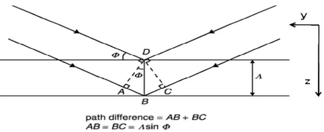
propagation constant and Ω is the non-zero residue phase at the z-axis origin. In the eqn (2.5-2), θ express the relative phase difference between perturbations of the refractive index and amplitude gain. Assume there is an incident plane wave entering the periodic, lossless waveguide at an angle of Φ as shown in Fig. 2.2. The propagation constant of the wave is assumed to beβ . 0
9
At each periodic interval of Λ, the incident wave will experience the same degree of
refractive index change so that the incident wave will be reflected in the same direction. For a waveguide that consists of N periodic corrugations, there will be N reflected wavelets. In order that any two reflected wavelets add up in phase or interfere constructively, the phase difference between the reflected wavelets must be a multiple of 2π. In other words,
β (AB BC) β (2 sin ) 2mπ
0
0 + = Λ Φ = (2.6)
where m is an integer. If the incident wave is now approaching more or less at a right angle to the wavefront (i.e. Φ≈π2), eqn (2.6) becomes
2β0Λ =2mπ (2.7) This is known as the Bragg condition andβ becomes the Bragg propagation 0
constant. The integer m shown in the above equation defines the order of Bragg diffraction. Unless otherwise stated, first-order Bragg resonance (m =1) is assumed. Since a laser forms a resonant cavity, the Bragg condition must be satisfied [8]. Rearranging eqn (2.7) gives
Λ = ≡ ≡ π λ π β c w n n B B 0 0 0 2 (2.8)
where λB and w are the Bragg wavelength and the Bragg frequency, respectively. B
From eqn (2.8), it is clear that the Bragg propagation constant is related to the grating period. By altering the grating period, the Bragg wavelength can be shifted according to the specific application.
Using small signal analysis, the perturbations of the refractive index and gain are always smaller than their average values, i.e.
0 n n<<
Δ , Δα <<α0 (2.9)
10 ) 2 cos( ] [ 2 2 ) ( 0 0 0 0 0 0 0 0 0 0 2 = 2 2+ + + Δ +Ω z n j n k k n k j n k z k α α β +2jk0n0Δαcos(2β0z+Ω+θ) (2.10)
With k0n0 replaced by β and α0<β , the above equation becomes
(2 0 ) 0 2 2 ] 2 [ 2 2 ) (z ≈ + j + Δn+ jΔ ej ej z+Ω k α θ β λ π β βα β ] (2 0 ) 2 [ 2 Δ + Δ − − +Ω + n j α e jθ e j β z λ π β (2.11)
For the case when θ=0 , one can simplify (2.10) to[10]
) 2 cos( 2 4 2 0 0 2 2 +Ω ⎥⎦ ⎤ ⎢⎣ ⎡ Δ + Δ + + ≈ j n j z k α β λ π β βα β (2.12)
By controlling all the perturbed terms, one can define a parameter k[8,10] such that
k
=
Δ
n
+
j
Δ
=
k
i+
jk
g2
α
λ
π
(2.13) Here k includes all contributions from the refractive index perturbation iwhilstk covers all contributions from the gain perturbation. The parameter k g
introduced in the above equation is known as the coupling coefficient. After a series of simplifications, eqn (2.12) becomes
) 2 cos( 4 2 0 0 2 2 ≈ + j + k z+Ω k β βα β β (2.14) On substituting the above equation back into the wave equation, one ends up with
0 } 2 2 2 { (2 0 ) (2 0 ) 0 2 2 2 = + + + + j k e +Ω k e− +Ω E dz E d β βα β j β z β j β z (2.15)
where the cosine function shown in eqn (2.14) has been expressed in phasor form. A trial solution of the scalar wave equation could be a linear superposition of two opposing traveling waves such that
jkunz jkunz B z e e z A z E( )= ( ) − + ( ) (2.16) with 2 0 0 2 2 β 2jβα (β jα ) k un = + ≈ + (Qα0<<β) (2.17)
In order to satisfy the Bragg condition shown earlier in eqn (2.8), the actual propagation constant,β , should be sufficiently close to the Bragg propagation
11
constant, β , to make the absolute difference between them much smaller than the 0
Bragg propagation constant. In other words,
0 0 β β
β − << (2.18) Such a difference between the two propagation constants is commonly known as the detuning factor or detuning coefficient, δ , which is defined as
δ =β −β0 (2.19)
The trial solution can be expressed in terms of the Bragg propagation constant, i.e.
z j z j z j z z j ze D z e e R z e S z e e z C z E( )= ( ) −δ − β0 + ( ) δ β0 = ( ) − β0 + ( ) β0 (2.20) where R(z) and S(z) are complex amplitude terms. Since the grating period Λ in a DFB semiconductor laser is usually fixed and so is the Bragg propagation constant, it is more convenient to consider eqn (2.20) as the trial solution of the scalar wave equation. By substituting eqn (2.20) into eqn (2.15), one ends up with the following equation R j R R R j R e j 0z 0 2 2 0 0 ' 2 ) 2 " ( − β −β +β + βα − β z j e S j S S S j S 0 0 2 2 0 0 ' 2 ) 2 " ( + β −β +β + βα β + 0 ) (Re ) ( 2 2 0 + 2 0 ⋅ 0 + 0 = + kβ e jβ zejΩ e− jβ ze−jΩ −jβ z Sejβ z (2.21)
where R’ and R” are the first- and second-order derivatives of R. Similarly, S’ and S” represent the first- and second-order derivatives of S. With a ‘slow’ amplitude approximation, high-order derivatives like R’’ and S’’ become negligible when compared with their first-order terms. By separating the above equation into two groups, each having similar exponential dependence, one can get the following pair of coupled wave equations
− Ω − = + − j R jkSe j dz dR ) (α0 δ (2.22) Ω − = + j S jk j dz dS Re ) (α0 δ (2.23)
12
Equation (2.22) collects all the exp(- jβ ) phase terms propagating along the 0z
positive z direction, whilst eqn (2.23) gathers all the exp( jβ ) phase terms 0z
propagating along the negative direction. Since δ << , other rapidly changing β phase terms such as exp(± j3β0z) have been dropped. In deriving the above
equations, the following approximation has been assumed
δ β β β β β − ≈ − = 0 0 2 0 2 2 (2.24) Following the above procedures, one ends up with a similar pair of coupled wave equations for a non-zero relative phase difference between the refractive index and the gain perturbation (i.e. θ ≠0) such that
Ω − − = + − j RS jk R j dz dR Re ) (α0 δ (2.25) Ω − = + j SR jk S j dz dS Re ) (α0 δ (2.26) where
k
RS=
k
i+
jk
ge
−jθ (2.27)is the general form known as the forward coupling coefficient and
θ j g i SR
k
jk
e
k
=
+
(2.28) is the backward coupling coefficient.It is contrary to Fabry Perot lasers, where optical feedback is come from the laser facets. Optical feedback in DFB lasers is originated from along the active layer where corrugations are fabricated. From the above scalar equation, the couple-wave equation can be established in the general form, which is for one dimensional situation. Following we will discuss two dimensional optical coupling based on above couple- wave theory. For our GaN-based photonic structure, we assume that since the carriers in the InGaN layers are confined in the wall, they do posses a significant in-plane dipole, which can couple to TE mode. Therefore, we centered on TE like mode in
13
square lattice for 2D case.
2.2 2D couple-wave model
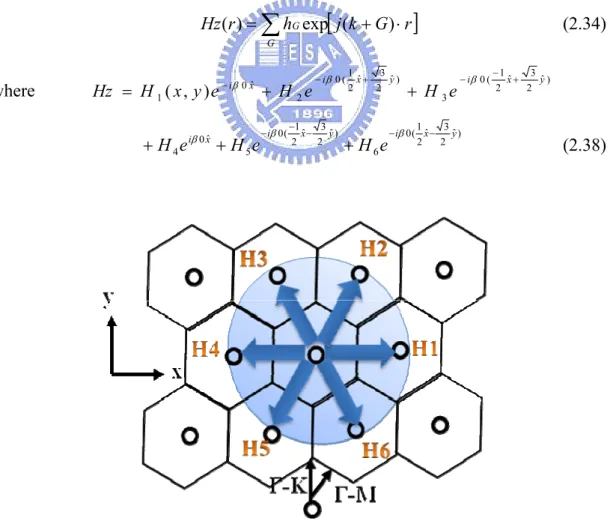
Preliminary numerical works have been done by Sakai, Miyai, and Noda [12,13]. Here, we cite their papers as references to help us understand the 2D couple-wave model. The 2D PC structure investigated here consists of an infinite square lattice with circular air holes in the x and y directions, as shown in Fig 2.3. The structure is assumed to be uniform in the z direction. We don’t consider the gain effects during calculation. We do calculate the resonant mode frequency as a function of coupling coefficient. The scalar wave equation for the magnetic field Hz in the TE mode can be written as [14] 2 0 2 2 2 2 = + ∂ ∂ + ∂ ∂ Hz k y Hz x Hz (2.30) where [15]
∑
[
]
≠ ⋅ + + = 0 2 2 2 2 ( )exp ( ) G r G j G k j k β αβ β (2.31)G=(mβ0, nβ0) is the reciprocal lattice vector, m and n are arbitrary integers, a
π
β0=2 where a is the lattice constant,
c w nav
=
β where navis the averaged
refractive index, k(G)=πnGλ is the coupling constant, where nG is the Fourier
coefficient of the periodic refractive-index modulation and λ is the Bragg wavelength given by λ =anav. In the eqn (2.31), we set α,αG<<β0,nG<<n0. We
do consider Γ point, in which when it is satisfy the second order Bragg diffraction , it will induce 2D optical coupling and result in surface emission. The coupling constant )κ(G can be expressed as
( ) 2 1 ) ( ) (G n G j α G λ π κ = + (2.32) where )n(G is the Fourier coefficient of periodic refractive index modulation and
14
Figure 2.3 Schematic diagram of eight propagation waves in square lattice PC structure
In eqn (2.31), the periodic variation in the refractive index is included the small perturbation in third term through the Fourier expansion. In the Fourier expansion, the periodic perturbation terms generates an infinite set of diffraction orders. However, as the cavity mode frequency is sufficient close to the Bragg frequency, only the second order diffraction and below can do significant contribution, others can consider to be neglected. Therefore, we focus on diffraction order with m + n ≤2 to discuss. The corresponding coupling coefficient constant jκ (j=1, 2, 3) are denoted as
κ1=κ(G)G =β0 0 2 κ( ) 2β κ = G G = (2.33) 0 3 κ( ) 2β κ = G G =
while considering infinite structure, the magnetic field can be described by the Bloch mode [14], =
∑
[
+ ⋅]
G G j k G r h r Hz( ) exp ( ) (2.34) Gh is the amplitude of each plane wave, k is the wave vector in the first Brillouin zone and when it is the Г point, it comes to zero. However, in the case of finite structure,
G
15
propagating waves in PC structure denoted as Rx, Sx, Ry, Sy, F1, F2, F3, F4 showed in
Fig 2.3, those are the amplitudes of four propagating waves in the x, -x, y, -y directions and four propagating waves in Г-M direction, respectively. Those correspond to hG in eqn (2.34). Here, we do consider these basic wave vectors
along the Г-X directions with κ+ G =β0and Г-M directions withκ+ G = 2β0.
The contribution of the higher order waves with κ+ G ≥2β0, are considered to be
negligible. We should note that the basic waves and higher order waves are partial waves of the Bloch mode, so they have the same eigenvalue β for specific resonant cavity mode.
The magnetic field in this case can be rewritten as
Hz =Rx(x,y)e−jβ0x +Sx(x,y)ejβ0x +Ry(x,y)e−jβ0y +Sy(x,y)ejβ0y F ej x j y F e j x j y F ej x j y F e j 0x j 0y 4 0 0 3 0 0 2 0 0 1 β +β + −β + β + β −β + −β −β + (2.35)
Put eqn (2.35) and eqn (2.31) into the wave eqn (2.30), and comparing the equal exponential terms, we obtain eight wave equations
(β−β0)Rx+κ3Sx−κ1(F2+F4)=0 (2.36a) (β−β0)Sx+κ3Rx−κ1(F1+F3)=0 (2.36b) (β −β0)Ry+κ3Sy−κ1(F3+F4)=0 (2.36c) 0 ) ( ) (β −β0 Sy+κ3Ry−κ1 F1+F2 = (2.36d) ( ) 0 2 ) 2 (β − β0 F1−κ1 Sx+Sy = (2.36e) ( ) 0 2 ) 2 (β− β0 F2−κ1 Rx+Sy = (2.36f) ( ) 0 2 ) 2 (β − β0 F3−κ1 Sx+Ry = (2.36g) ( ) 0 2 ) 2 (β − β0 F4 −κ1 Rx+Ry = (2.36h)
In the above equations, we assumeβ/β0≈1, since we take optical coupling at Г point as an example.
16
These derivations illustrate the coupling among the propagating waves in square lattice PC structure. We take eqn (2.36) for example. It describes the net wave superposition along the x-axis, including the coupling of two waves propagating at opposite directions, Rx and Sx, with a coupling coefficient κ . And the coupling of 3
higher order waves F2 and F4, with a coupling coefficient κ1. The coupling κ 3
provides the main distributed feedback. From above derivations, we know that the orthogonal couplings occur via intermediate coupling of the basic and higher order waves. One thing we should noted that the coupling coefficient κ2 does not exist in
eqn (2.36). In the numerical view which describes the basic waves directly couple to orthogonal directions. This physically can be explained in this way: ways of TE modes have their electric field parallel to the PC plane, so that the electric field directions of the two waves propagating in the perpendicular directions are orthogonal to one another, hence the overlap integral of the two waves vanishes.
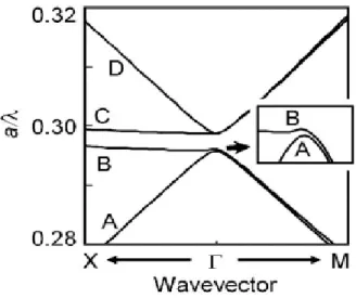
By using 2D plane wave expansion method, the band dispersion curves for TE like modes in Fig 2.4 can be obtained. The condition is limited at the vicinity near Bragg frequency.
Figure 2.4 Dispersion relationship for TE like modes, calculated using the 2D PWEM
17
cavity mode frequencies denoted as wA wB wC wD, with one degenerated.
) 2 2 8 1 )( ( 3 0 2 1 3 0 κ β κ κ β − − − = av A n c w ( ) 3 0 κ β − = av B n c w ) 2 2 4 1 )( ( 3 0 2 1 3 0 , κ β κ κ β − − + = av D C n c w (2.37)
The frequencies wA and wB at the lower band-edges are non-degenerated, while
two of the frequencies wc and wD at higher band-edge are degenerated. In the
physical meaning, the resonant mode symmetries are different. The resonant mode at band-edge C and D are symmetric, which allows this mode to couple to external field more easily. The characteristics of these resonant modes are essentially leaky [16]. The resonant mode at band-edge A and B are anti-symmetric, resulting in less coupling to the external field. Therefore, the quality factor for band-edge A and B are higher than C and D. It is expected that the lasing behavior is occurred at either A or B. However, band B is flat around Г point in the Г-X direction. Light at band-edge B can couple to leaky mode with a wave vector slightly shifted from Г point, resulting in coupling to the external field. Thus, band-edge B becomes leaky.
So far we have understood the fundamental couple-wave theory and how to calculate their cavity mode frequency. For our GaN-based PCSELs, we design the triangular lattice with TE-like mode to tell the differences between square lattice structure. Therefore, in next section, we develop a new model to explain the DFB feedback mechanism based on couple-wave theory. According to our measurement, we found that the lasing action occurred at Г1, K2, M3 point band-edges. We tried to solve the wave equations at these band-edges and derive the coupling coefficients. All of detail will be described numerically in next section.
18
2.3 Couple-wave model for triangular lattice PCSELs
Light at the photonic band-edge has zero group velocity and forms a standing wave due to 2D DFB effect. Laser oscillation is expected to occur at any band-edge, if the gain threshold is achieved. Therefore, we focus on the coupling waves at Г1, K2, M3 band-edges according to our lasing behaviors.
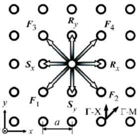
I. Г1 numerical results
The 2D PC structure investigated here consists of an infinite triangular lattice with circular air holes in the x and y directions, as shown in Fig 2.5. The structure is assumed to be uniform in the z direction. We don’t consider the gain effects during calculation. While considering infinite structure, the magnetic field can be described by the Bloch mode [14],
=
∑
[
+ ⋅]
G G j k G r h r Hz( ) exp ( ) (2.34) where 2 ˆ) 3 ˆ 2 1 ( 0 3 ) ˆ 2 3 ˆ 2 1 ( 0 2 ˆ 0 1( , ) y x i y x i x i H e H e e y x H Hz + − − + − − + + = β β β 0(21ˆ 23ˆ) 6 ) ˆ 2 3 ˆ 2 1 ( 0 5 ˆ 0 4 y x i y x i x i H e H e e H − − − − − + + + β β β (2.38)Figure 2.5 Schematic diagram of six propagation waves in triangular lattice for Г1 point
19
exponential terms, we obtain six wave equations
4 3 5 3 2 6 2 1 1 1 ( ) 2 ) ( 2 ) ( i H i H H i H H i H H x κ κ κ δ α − =− + + + + − + ∂ ∂ − (2.39a) 5 3 6 4 2 3 1 1 2 2 2 ( ) 2 ) ( 2 ) ( 2 3 2 1 H i H H i H H i H i H y H x κ κ κ δ α− =− + + + + − + ∂ ∂ − ∂ ∂ − (2.39b) 6 3 5 1 2 4 2 1 3 3 3 2 ( ) 2 ( ) 2 ( ) 3 2 1 H i H H i H H i H i H y H x κ κ κ δ α− =− + + + + − + ∂ ∂ − ∂ ∂ − (2.39c) 1 3 6 2 2 5 3 1 4 4 ( ) 2 ) ( 2 ) ( i H i H H i H H i H H x κ κ κ δ α − =− + + + + − + ∂ ∂ (2.39d) 2 3 3 1 2 6 4 1 5 5 5 2 ( ) 2 ( ) 2 ( ) 3 2 1 H i H H i H H i H i H y H x κ κ κ δ α− =− + + + + − + ∂ ∂ + ∂ ∂ (2.39e) 3 3 4 2 2 5 1 1 6 6 6 ( ) 2 ) ( 2 ) ( 2 3 2 1 H i H H i H H i H i H y H x κ κ κ δ α− =− + + + + − + ∂ ∂ + ∂ ∂ − (2.39e)
where, H1, H2, H3, H4, H5, and H6 express the envelope magnetic field distributions
of individual light waves propagating in the six equivalent Г-M directions: 0°, +60°, +120°,+180°, +240°, and +300° with respect to the x-axis. κ1, κ2, and κ3 are the
coupling coefficients between light waves propagating at 60° to each other (H1 and H2,
H2 and H3,and so on), at 120° (H1 and H3, H2 and H4, and so on), and at 180° (H1 and
H4, H2 and H5, and so on), respectively. δ is the deviation of the wave number β
(expressed as 2πν/c, where ν is the frequency and c is the velocity of light) from the fundamental propagation constant β0 (equal to 4π 3a, where a is the lattice
constant) for each cavity mode, and expressed as δ =(β2 −β02)/2β0, α is the
corresponding threshold gain.
By solving eqn (2.39a-e), a cavity frequency ν for each band-edge mode and the corresponding threshold gain α for a given set of coupling coefficients, κ1, κ2,
and κ3, can be obtained. When only the cavity mode frequencies are required, the
derivation terms and the threshold gain α in eqn (2.39a-e) can be set to zero, and the individual cavity frequencies can then be derived as follows:
20 ) ( 2 0 1 2 3 1 π β κ κ κ ν = − − + neff c (2.40a) ) 2 1 2 1 ( 2 0 1 2 3 2 π β κ κ κ ν = − + − neff c (2.40b) ) ( 2 0 1 2 3 3 π β κ κ κ ν = + − − neff c (2.40c) ) 2 1 2 1 ( 2 0 1 2 3 4 π β κ κ κ ν = + + + neff c (2.40d) where, c is the velocity of a photon in vacuum, and neff is the effective refractive index
of the device structure. There are four cavity mode frequencies, ν1 −ν4 , which correspond to the four band-edge, including two degenerate modes ν and 2 ν . 4 Once the cavity mode frequency at the individual band-edges can be obtained, we can derive the coupling coefficientsκ1, κ2, and κ3 from eqn (2.40a-d) as follows:
0 4 3 2 1 4 3 2 1 1 2 2 2ν ν ν β ν ν ν ν ν κ + + + + + − − = (2.41a) 0 4 3 2 1 4 3 2 1 2 2 2 2ν ν ν β ν ν ν ν ν κ + + + + − + − = (2.41b) 0 4 3 2 1 4 3 2 1 3 2 2 2 2 2 β ν ν ν ν ν ν ν ν κ + + + + − − = (2.41c)
By comparing the value of coupling coefficientsκ1, κ2, and κ3 based on actual
device parameters, we can determine which kind of DFB mechanism provide the
major significant contribution to support the lasing oscillation.
II. K2 numerical results
The 2D PC structure investigated here consists of an infinite triangular lattice with circular air holes in the x and y directions, as shown in Fig 2.6. The structure is assumed to be uniform in the z direction. We don’t consider the gain effects during calculation. While considering infinite structure, the magnetic field can be described by the Bloch mode [14],
=
∑
[
+ ⋅]
G G j k G r h r Hz( ) exp ( ) (2.34)21 where 2 ˆ) 3 ˆ 2 1 ( 0 3 ) ˆ 2 3 ˆ 2 1 ( 0 2 ˆ 0 1 y x i y x i x i
H
e
H
e
e
H
Hz
− − − + − − −+
+
=
β β β (2.42)Figure 2.6 Schematic diagram of three propagation waves in triangular lattice for K2 point
put eqn (2.42) and eqn (2.31) into the wave eqn (2.30), and comparing the equal exponential terms, we obtain three wave equations :
) ( 2 ) ( 1 2 3 1 i H i H H H x + − − = + ∂ ∂ − α δ κ (2.43a) ) ( 2 ) ( 2 3 2 1 3 1 2 2 2 H i H i H H y H x ∂ + − − = + ∂ − ∂ ∂ − α δ κ (2.43b) ) ( 2 ) ( 2 3 2 1 2 1 3 3 3 H i H i H H y H x ∂ + − − = + ∂ + ∂ ∂ α δ κ (2.43c) where, H1, H2, H3 express the envelope magnetic field distributions of individual
light waves propagating in the three equivalent Г-K directions: 0°, 120°, 240° with respect to the x axis. κis the coupling coefficient between light waves propagating at 120° to each other (H1 and H2, H2 and H3, H1 and H3), δ is the deviation of the
wave number β (expressed as 2πν/c, where ν is the frequency and c is the velocity of light) from the fundamental propagation constant β0 (equal to 8π/3a,
where a is the lattice constant) for each cavity mode, and expressed as
0 0
2 2)/2
(β β β
22
By solving eqn (2.43a-c), a cavity frequency ν for each band-edge mode and the corresponding threshold gain α for a given set of coupling coefficients, κ can be obtained. When only the cavity mode frequencies are required, the derivation terms and the threshold gain α in eqn (2.39a-e) can be set to zero, and the individual cavity frequencies can then be derived as follows:
) 0 ( 2 1 β κ π ν = − neff c (2.44a) ) 2 1 0 ( 2 2 β κ π ν = + neff c (2.44b) where, c is the velocity of a photon in vacuum, and neff is the effective refractive index
of the device structure. There are two cavity mode frequencies, ν1,ν2 , which correspond to the two band-edge, including one degenerate modes ν . Once the 2 cavity mode frequency at the individual band-edges can be obtained, we can derive the coupling coefficientsκfrom eqn (2.44a,b) as follows:
0 2 1 1 2 2 2ν β ν ν ν κ + − = (2.45)
From the 2D couple-wave model, we know light at K2 band-edge can couple to each other and form the triangular feedback close loop via DFB effect.
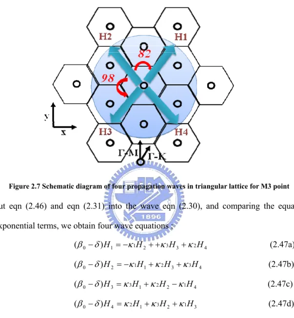
III. M3 numerical results
The 2D PC structure investigated here consists of an infinite triangular lattice with circular air holes in the x and y directions, as shown in Fig 2.7. The structure is assumed to be uniform in the z direction. We don’t consider the gain effects during calculation. While considering infinite structure, the magnetic field can be described by the Bloch mode [14],
=
∑
[
+ ⋅]
G G j k G r h r Hz( ) exp ( ) (2.34) whereHz
=
H
1+
H
2+
H
3+
H
4 (2.46)23
Actually we can easily derive the couple-wave equations. Therefore, the phase term will not describe in detail.
Figure 2.7 Schematic diagram of four propagation waves in triangular lattice for M3 point
put eqn (2.46) and eqn (2.31) into the wave eqn (2.30), and comparing the equal exponential terms, we obtain four wave equations :
4 2 3 3 2 1 1 0 ) (β −δ H =−κ H ++κ H +κ H (2.47a) 4 3 3 2 1 1 2 0 ) (β −δ H =−κ H +κ H +κ H (2.47b) 4 1 2 2 1 3 3 0 ) (β −δ H =κ H +κ H −κ H (2.47c) 3 1 2 3 1 2 4 0 ) (β −δ H =κ H +κ H +κ H (2.47d) where, H1, H2, H3, H4 express the envelope magnetic field distributions of individual
light waves propagating in the four directions: κ1, κ2, and κ3 are the coupling
coefficients between light waves propagating at 82° to each other (H1 and H2, H3 and
H4), at 98° (H1 and H4, H2 and H3), and at 180° (H1 and H3, H2 and H4), respectively.
δ is the deviation of the wave number β (expressed as 2πν/c, where ν is the frequency and c is the velocity of light) from the fundamental propagation constant β0 (equal to 4.7π 3a, where a is the lattice constant) for each cavity mode, and
24
expressed as δ =(β2 −β02)/2β0, α is the corresponding threshold gain
By solving eqn (2.47a-d), a cavity frequency ν for each band-edge mode and the corresponding threshold gain α for a given set of coupling coefficients, κ1, κ2,
and κ3, can be obtained. When only the cavity mode frequencies are required, the
derivation terms and the threshold gain α in eqn (2.39a-e) can be set to zero, and the individual cavity frequencies can then be derived as follows:
) ( 2 0 1 2 3 1 π β κ κ κ ν = + − − neff c (2.48a) ) ( 2 0 1 2 3 2 π β κ κ κ ν = − + − neff c (2.48b) ) ( 2 0 1 2 3 3 π β κ κ κ ν = − − + neff c (2.48c) ) ( 2 0 1 2 3 4 π β κ κ κ ν = + + + neff c (2.48d) where, c is the velocity of a photon in vacuum, and neff is the effective refractive index
of the device structure. There are four cavity mode frequencies, ν1 −ν4 , which correspond to the four band-edge. Once the cavity mode frequency at the individual band-edges can be obtained, we can derive the coupling coefficientsκ1, κ2, and κ3
from eqn (2.40a-d) as follows
0 4 3 2 1 4 3 2 1 1 β ν ν ν ν ν ν ν ν κ + + + + − − = (2.49a) 0 4 3 2 1 4 3 2 1 2 β ν ν ν ν ν ν ν ν κ + + + + − + − = (2.49b) 0 4 3 2 1 4 3 2 1 3 β ν ν ν ν ν ν ν ν κ + + + + + − − = (2.49c)
By comparing the value of coupling coefficientsκ1, κ2, and κ3 based on actual
device parameters, we can determine which kind of DFB mechanism provide the most
significant contribution to support the lasing oscillation.
So far, the couple-wave model for different band-edge has been established. For next section, Bragg diffraction in different band-edge will be discussed to confirm the 2D
25
model we formed.
2.4 Bragg diffraction in 2D triangular lattice
[17,18]Fig 2.8a shows a band diagram of a triangular-lattice photonic crystal. The points I, II, and III are the points Γ1, M1, and K1, respectively. The reciprocal space of the
structure is a space combined by hexagons. Fig 2.8b shows a schematic diagram of a reciprocal space. The K1 and K2 are the Bragg vectors with the same magnitude,
|K|=2π/a, where a is the lattice constant of the photonic crystal. Consider the TE modes in the 2-D photonic crystal structure, the diffracted light wave from the structure must satisfy the relationship:
... , 2 , 1 , 0 q , K q K q k kd = i + 1 1 + 2 2 1,2 = ± ± i d =ω ω
where kd is xy-component wave vector of diffracted light wave, ki is xy-component
wave vector of incident light wave, q1,2 is order of coupling, ωd is the frequency of
diffracted light wave, and ωi is the frequency of incident light wave.
Figure 2.8a The band diagram of a triangular lattice photonic crystal
(2.22) (2.21) 0.0 0.1 0.2 0.3 0.4 0.5 0.6 0.7 0.8
No
rm
al
iz
ed fr
equ
en
cy
(a/
λ)
ΓM K
ΓI
II
II
IV
26
Figure 2.8b The schematic diagram of a reciprocal space
It is expected lasing occurs at specific points on the Brillouin-zone boundary (Γ, M, and K) and at the points at which bands cross and split. At these lasing points, waves propagating in different directions couple to significantly increase the mode density. It is particularly interesting that each of these points exhibits a different type of wave coupling. For example, as shown in Fig 2.9a, the coupling at point I only involves two waves, propagating in the forward and backward directions. This coupling is similar to that of a conventional DFB laser. However, there can be six equivalent Γ-M directions in the structure; that is, the cavity can exist independently in each of the three different directions to form three independent lasers. Point II has a unique coupling characteristic unachievable in conventional DFB lasers, the coupling of waves propagating in three different directions as shown in Fig 2.9b. This means the cavity is a triangular. In fact, there can also be six Γ-K directions in the structure; therefore, two different lasing cavities in different Γ-K directions coexist independently. At point III the coupling includes waves in in-plane all six directions; 0°, 60°, 120°, -60°, -120°, and 180° as shown in Fig 2.9c. In addition, the coupled light can be emitted perpendicular from the surface according to first order Bragg diffraction, as shown in Fig 2.10. This is the same phenomenon that occurs in conventional grating-coupled surface-emitting lasers.
K1 K2 Γ M K K1 K2 Γ M K
(B)
27
Figure 2.9 Wave vector diagram at (A) point I (B) point II (C)point III , ki and kd indicate incident and diffracted light wave
Γ K2 ki kd=ki+K2 X Y K1 kd=ki+K1 K K Γ K2 ki kd=ki+K2 X Y K1 kd=ki+K1 K K
II
Γ K1 ki kd=ki+K1 X Y M kd=ki-K1 Γ K1 ki kd=ki+K1 X Y M kd=ki-K1I
III
28
Figure 2.10 The wave vector diagram at point III in vertical direction
The device, therefore, functions as a surface emitting lasers.Fig 2.11a and Fig 2.11b show the in-plane and vertical diffraction at point IV. In this case, the light wave is diffracted in five Γ-K directions and in the vertical direction similar to point III, and Ki+q1K1+q2K2 reaches the six Γ’ points. Fig 2.11c shows the wave-vector diagram of oneΓ’ point where the light wave is diffracted in an oblique direction. The light wave is also diffracted in a bottom oblique direction. The same diffraction phenomena occur at the other five G8 points, resulting in diffraction in 19 directions at point IV.
29
Figure 2.11 Wave vector diagram of (A) in-plane and (B) vertical direction at point IV (C) Wave vector diagram showing diffraction in an oblique direction at point IV.
30
References
1. M. Imada, S. Noda, A. Chutinan, T. Tokuda, M. Murata, and G. Sasaki, Appl.
Phys .Lett. 75, 316 (1999)
2. S. Noda, M. Yokoyama, M. Imada, A. Chutinan, and M. Mochizuki, Science 293,
1123 (2001)
3. H. Y. Ryu, S. H. Kwon, Y. J. Lee, and J. S. Kim, Appl. Phys. Lett. 80, 3467
(2002)
4. G. A. Turnbull, P. Andrew, W. L. Barns, and I. D. W. Samuel, Appl. Phys. Lett. 82,
313 (2003)
5. K. Sakai, E. Miyai, T. Sakaguchi, D. Ohnishi, T. Okano, and S. Noda, IEEE J. Sel.
Areas Commun. 23, 1335-1340 (2005)
6. M. Imada, A. Chutinan, S. Noda and M. Mochizuki Phys. Rev. B 65, 195306 1-8
(2002)
7. M. Yokoyama and S. Noda Opt. Express 13, 2869-2880 (2005)
8. H. Kogelnik and C. V. Shank Appl. Phys. Lett. 43, 2327-2335 (1972)
9. Distributed Feedback Laser Diodes and Optical Tunable Filters
10. Streifer, W., Burnham, R.D.and Scifres, D.R. IEEE J. Quantum Electron. QE11(4),
154-161 (1975).
11. David, K. IEEE J. Quantum Electron.27(6), 1714-1724, 1991
12. Kyosuke Sakai, Eiji Miyai and Susumu Noda Optics Express Vol. 15, 3981,
(2007)
13. Kyosuke Sakai, Eiji Miyai and Susumu Noda APL , 89, 021101 (2006)
14. Plihal and A. A. Maradudin, Phys. Rev. B, 44, 8565 (1991)
15. H. Kogelnik, Bell Syst. Tech. J. 48, 2909 (1969)
16. T. Ochiai and K.Sakoda Phys. Rev. B 63, pp. 125 107-1-125 107-7, (2001)
31
32
Chapter 3
Fabrication of Nitride-based 2D
Photonic Crystal
Surface Emitting Lasers
Introduction
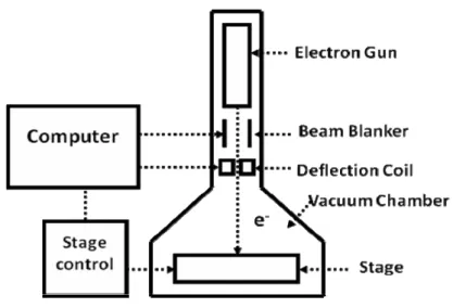
Currently, photonic crystals, which are periodic patterns with sizes of sub-micrometer, are usually fabricated using electron-beam lithography. The electron-beam lithography (EBL) is a technique using electron beam to generate patterns on a surface with a resolution limited by De Broglie relationship (λ < 0.1 nm for 10-50 KeV electrons), which is far smaller than the light diffraction limitation. Therefore, it can beat the diffraction limit of light to create a pattern which only has a few nanometers line-width without any mask. The first EBL machine, based on SEM system, was developed in the 1960s. The EBL system usually consists of an electron gun for generating electron beam, a beam blanker for controlling the electron beam, electron lenses for focusing the electron beam, a stage and a computer control system as shown in Fig 3.1.
Figure 3.1 The typical schematic diagram of EBL system
33
3.1 Wafer Preparation
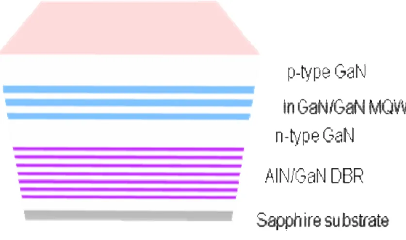
The nitride heterostructure of GaN-based MCLED was grown by metal-organic chemical vapor deposition (MOCVD) system (EMCORE D-75) on the polished optical-grade c-face (0001) 2’’ diameter sapphire substrate, as shown in Fig. 3.2a. Trimethylindium (TMIn), Trimethylgallium (TMGa), Trimethylaluminum (TMAl), and ammonia (NH3) were used as the In, Ga, Al, and N sources, respectively. Initially,
a thermal cleaning process was carried out at 1080°C for 10 minutes in a stream of hydrogen ambient before the growth of epitaxial layers. The 30nm thick GaN nucleation layer was first grown on the sapphire substrate at 530oC, then 2µm thick undoped GaN buffer layer was grown on it at 1040oC. After that, a 35 pairs of quarter-wave GaN/AlN structure was grown at 1040oC under the fixed chamber
pressure of 100Torr and used as the high reflectivity bottom DBR. Finally, the 5λ active pn-junction region was grown atop the GaN/AlN DBR, composed typically of ten In0.2Ga0.8N quantum wells (LW=2.5 nm) with GaN barriers (LB=7.5 nm), and
surrounded by 560nm thick Si-doped n-type GaN and 200nm thick Mg-doped p-type GaN layers. The reflectivity spectrum of the half structure with 35 pairs of GaN/AlN DBR structure was measured by the n&k ultraviolet-visible spectrometer with normal incident at room temperature, as shown in Fig. 3.2.b The reflectivity spectrum centered at 430nm and stopband width of about 28nm. Fig. 3.2.c shows the PL spectrum of our as grown sample.
34 360 380 400 420 440 460 480 500 520 0 20 40 60 80 100 Reflectance% Wavelength(nm)
Figure 3.2b Reflectivity spectrum of the half structure with 35 pairs of GaN/AlN DBR structure measured by N&K ultraviolet-visible spectrometer with normal incident at room temperature.
Figure 3.2c The u-PL spectrum of as-grown sample
380
400
420
440
460
480
0.0
0.5
1.0
1.5
2.0
2.5
3.0
@~425nmInt
e
ns
ity
(arb. u
nit
)
Wavelength(nm)
25nm
35
3.2 Process Procedure
There are some principles to fabricate GaN-based PCSELs, including initial clean (I.C.), plasma enhanced chemical vapour deposition (PECVD) technique, EBL technique and inductively coupled plasma - reactive ion etching (ICP-RIE) technique. The purpose of the I.C. is to remove the small particle and organism on the sample surface. The steps of I.C. are described as below.
Initial clean (I.C.)
1. Degreasing particles in acetone (ACE) 5min by ultrasonic baths.
2. Dipping in isopropyl alcohol (IPA) 5min by ultrasonic baths for organism removed.
3. Rising in de-ionized water (D.I. water) 5min for surface clean. 4. Blowing with N2 gas for surface drying.
5. Baking by hot plate 120oC, 5min, for wafer drying.
PECVD (SAMCO PD220)
The purpose of PECVD technique is to deposit a SiN film for hard mask. The details of PECVD parameters are expressed as below.
1. Initial clean
2. SiN film deposition : SiHl4/Ar : 20sccm NH3 : 10sccm N2 : 490sccm Temperature : 300℃ RF power : 35W Pressure :100Pa
Time : 20min for depositing SiN 200nm
EBL
The purpose of the EBL is to define the PC pattern on the photoresist (PMMA) (soft mask). In the process of EBL, a special positive photoresist PMMA (A3) was used. These EBL parameters are described as below.
1. Spin coating use the photoresist : PMMA (A3). a. first step : 1000 rpm for 10sec.
36
2. Hard bake : hot plate 180oC, 1hr.
3. Exposure :
Beam voltage : 10KeV Writefield size : 50μm
4. Development : dipping in IPA : MIBK(3 : 1) 50sec. 5. Fixing : rising in IPA 30sec.
6. Blowing with N2 gas for drying.
7. Hard bake : hot plate 120oC, 4min.
ICP-RIE (Oxford Plasmalab system 100)
The soft mask was transfered to SiN film to form the hard mask by using ICP-RIE. These ICP-RIE techniques are described as below.
1. SiN film etching: Ar/O2: 5sccm
CHF3: 50sccm
Forward power: 150W Pressure: 7.5*10-9Torr Temperature: 20℃
Time: 100 second for etching SiN film 200nm 2. Initial clean for remove soft mask
ICP-RIE (SAMCO RIE-101PH)
The purpose of the ICP-RIE techique is to form the PC layer on GaN. The hard mask was transferred to GaN by using ICP-RIE techique. Figure 3.3 are shown the SEM image of top view and cross section of completed 2D PCSELs, respectively. These ICP-RIE techniques are described as below.
1. P-GaN etching: Ar : 10sccm Cl2 : 25sccm ICP power : 200W Bias power : 200W Pressure : 0.33Pa