國 立 交 通 大 學
電信工程學系
碩 士 論 文
應用於語音之三階三角積分數位類比轉換
器
A 3
rd-order Delta-Sigma Digital to Analog
Converter for Audio Application
研究生:黃 介 仁
指導教授:洪 崇 智 教授
應用於語音之三階三角積分數位
類比轉換器
A 3
rd-order Delta-Sigma Digital to Analog Converter for
Audio Application
研 究 生:黃介仁 Student:Chieh-Jen Huang
指導教授:洪崇智 教授 Advisor:Prof. Chung-Chih Hung
國 立 交 通 大 學
電 信 工 程 學 系 碩 士 班
碩 士 論 文
A Thesis
Submitted to Department of Communication Engineering College of Electrical and Computer Engineering
National Chiao Tung University in Partial Fulfillment of the Requirements
for the Degree of Master of Science in Communication Engineering Septemper 2008 Hsinchu, Taiwan.
中華民國九十七年九月
應用於語音之三階三角積分數位
類比轉換器
研究生:黃介仁 指導教授:洪崇智 教授
國立交通大學
電信工程學系碩士班
摘要
近年來因為語音產品的蓬勃發展,如 MP3 隨聲聽等等,使得語音系統數位類 比轉換器成為一個重要的目標。而對於用電池運作的語音系統有幾個問題是我們 必須注意的。因為功率消耗會影響電池的壽命,所以必須把功率消耗設計的越小 越好。另外,為了達到多媒體產品的品質需求,此數位類比轉換器必須達到約 16 位元的高解析度。三角積分數位類比轉換器(Delta-Sigma D/A converter)是一種廣泛運用的 技術,它能夠達到高解析度、降低數位電路部份的操作速度、能夠緩和頻帶外 (out-of-band)濾波器的需求以及提高對時脈抖動(clock jitter)的免疫力。使 用直接電荷轉換的切換式電阻電容技術可以減少kT/C 雜訊和元件不匹配的影響 而不增加功率消耗,並且比直接電荷轉換切換式電容技術擁有較少的失真。資料 加權平均的演算法可以抑制電容之間的不匹配所造成的非線性度。 在此研究中我們將介紹一個 15 等級量化、三階的三角積分數位類比轉換 器,取樣頻率是 44.1 千赫茲,輸入訊號為 24 位元,因為超取樣倍率為 64 倍, 所以主要時脈操作在 2.8224 百萬赫茲,本次設計的晶片是由晶片中心(CIC)提供 的台積電(tsmc)標準 0.18 微米製程中實現。在 1.8 伏特的供應電壓下可達 87 分貝的動態範圍,並且消耗 8.25 毫瓦特。
A 3
rd-order Delta-Sigma Digital to Analog Converter for
Audio Application
Student:Chieh-Jen Huang Advisor:Prof. Chung-Chih Hung
Department of Communication Engineering National Chiao Tung University
Hsinchu, Taiwan
Abstract
Audio digital-to-analog converters (DAC) have played an important role recently with the rapid growth of the cellular phone and portable audio devices. There are some main issues for a battery-operated audio system. Power dissipation affects the battery life, so it must be as low as possible. A high resolution of about 16bits is required for the DAC to meet the quality of the media.
The delta-sigma D/A converters have been used extensively. It can achieve high resolution, reduce digital circuit speed, relax the requirements of the out-of-band filter, and enhance immunity to clock jitter. Using the direct charge transfer switched-RC (DCT-SRC) technique in the multi-bit reconstruction DAC can reduce kT/C noise and element mismatch without increasing power dissipation. And this kind of DCT-SRC DAC has smaller distortion than direct charge transfer switch capacitor DAC (DCT-SCDAC). The data weighted averaging algorithm restrains nonlinearity caused by the mismatch of capacitors.
A 15-level quantization, third-order delta-sigma DAC is presented. Its sampling rate is 44.1 kHz with 24-bit input. The main clock is 2.8224 MHz because of the 64X oversampling ratio. This DAC implemented in a TSMC 0.18um CMOS process achieved 87dB dynamic range (DR), while consuming 8.25mW from a 1.8V supply.
誌謝
首先感謝我的指導教授洪崇智老師,在我兩年的研究生活中提供良好的學習 環境,以及這段日子來對我的指導與照顧,並且在研究主題上給予我寬廣的發展 空間。同時我也要感謝在這碩士班兩年內曾經敎過我的每位老師,由於他們熱心 的教學,使我在短短的碩士班兩年內,學習如何設計並且製作數位、類比積體電 路。還有要感謝國家晶片系統設計中心提供先進的半導體製程,讓我有機會將所 設計的電路得以實現並完成驗證。 其次,我要感謝羅天佑學長、楊家泰學長、蔡宗諺學長、白逸維學長、廖德 文學長、邱建豪學長和高正昇學長在研究上的指導與幫助,透過和學長之間的討 論,使我的基礎觀念更加清楚紮實,並且教導我如何使用各種儀器,以及協助解 決量測時所遇到的問題。接著還要感謝夏竹緯、楊文霖、林永洲、郭智龍、邱楓 翔和張維欣等諸位同窗,與我在實驗室一同奮鬥,還有李尚勳、黃聖文、許新傑 和簡兆良等學弟的支持。 特別要感謝我的父母和家人,感謝他們提供了一個穩定且健全的環境,使我 無後顧之憂地完成我的學業。最後要感謝我的女朋友,感謝她一直默默的支持 我、鼓勵我,並在這段成長的路上與我相伴。 總而言之,我要感謝所有關心我、愛護我和曾經幫助過我的人,願我在未來 能有一絲的成就獻給最愛我的家人、老師以及朋友,謝謝你們。 黃介仁 國立交通大學 中華民國九十七年九月Table of Contents
Abstract (Chinese) I Abstract (English) II Acknowledgment III Table of Content VI List of Figures VIII List of Tables XI
Chapter 1 Introduction 1
1.1 Motivation ……….……….……… 1
1.2 Thesis Organization ……….……… 2
Chapter 2 Delta-Sigma Digital-to-Analog Converters 4
2.1 Oversampling ………...………..………... 4
2.2 Noise shaping …..………...……… 4
2.3 Comparison of One-bit and Multi-bit implementations .…...……….. 7
2.4 Oversampling delta-sigma DACs ….…..……… 9
Chapter 3 Implementation of the Digital circuits in ΔΣ DAC design 11
3.1 Interpolating filter design ………...……….... 11
3.1.1 1 bit to 24bit converter ………... 11
3.1.2 Principle of interpolation filter design ……..………..…... 11
3.1.3 Implementation of interpolation filter ……….………..…... 13
3.2 Delta-Sigma modulator design ..……… 18
3.3 Dynamic Element Matching …….…….………...… 22
3.3.1 Thermometer code encoder ………... 22
3.3.2 DWA (data weighted averaging) circuit ………...………..…... 23
Chapter 4 Implementation of the Analog circuits in ΔΣ DAC design 25
4.1 DAC circuits ……….………... 25
4.1.1 Conventional Switched-Capacitor DAC ……...………... 26
4.1.2 SCDAC using Direct-Charge-Transfer technique……....…………..…... 28
4.1.3 Other examples of DAC circuits ………... 30
4.2 Low-voltage circuit design issues..………...………. 35
4.2.2 Low-threshold voltage device ………...……… 36
4.2.3 Clock voltage doubler ……….………..……… 36
4.2.4 Clock Bootstrapping …………...……….. 38
4.2.5 Switched-RC technique …...…...……….. 39
4.3 Class AB amplifiers ………...………..………... 40
4.3.1 CMOS output stage …...……….. 41
4.3.2 Cross-Coupled quads ..………..………...…... 43
4.3.3 Adaptive biasing ..……...…………..………...…... 46
4.3.4 IQcontrol with translinear circuits ..……….………...…... 47
4.4 Analog implementation of the Delta-Sigma Audio DAC …….………...…... 55
Chapter 5 Conclusions 62
5.1 Conclusion ………..… 62
5.2 Future Works ……….. 62
List of Figures
Chapter 2Figure 2.1 Spectra of (a) a Nyquist sampling (b) an oversampling, and (c) an
oversampling with noise shaping ……….……… 5
Figure 2.2 Linear model of the modulator ………..… 5
Figure 2.3 Different orders of the noise-shaping transfer functions ………...… 6
Figure 2.4 Illustration of step mismatch in the D/A converter ……….... 8
Figure 2.5 Block diagram of a delta-sigma DAC …..………..…..…………... 9
Figure 2.6 Frequency spectra at different points of the delta-sigma DAC .…. 10 Figure 2.7 Unit-element DAC ……….….. 10
Chapter 3 Figure 3.1 Block diagram of interpolation filter ………..……… 11
Figure 3.2 Interpolator’s spectrum ……….……..………. 12
Figure 3.3 FIR structure …………...………. 13
Figure 3.4 Implemented interpolator …..………...… 13
Figure 3.5 Second half-band FIR filter ……….… 14
Figure 3.6 Frequency responses of HBF1 and HBF2 ...……….……… 15
Figure 3.7 Implemented sinc filter ……….... 16
Figure 3.8 Frequency response of sinc filter ……….……… 16
Figure 3.9 The frequency response of interpolation filter after synthesis …... 17
Figure 3.10 Delta-Sigma modulator architecture ……….. 18
Figure 3.11 Output of the modulator …... 20
Figure 3.12 Output spectrum of the modulator ………. ……....…….……. 21
Figure 3.13 Out-of-band spectrum of the modulator …………...……….. 21
Figure 3.14 The implementation of DEM process ………..…. 22
Figure 3.15 DWA operation ………..…….…
…
………….. 24Chapter 4 Figure 4.1 Block diagram of the analog part circuit ………... 25
Figure 4.2 (a) Conventional SCDAC1 (b) during φ1 phase (c) during φ2 phase ………..…….………... 26 Figure 4.3 (a) Conventional SCDAC2 (b) during φ1 phase (c) during φ2 phase
………..…….………... 27
Figure 4.4 Concept of the DCT-SC technique ………... …………... 28
Figure 4.5 Five-bit SCDAC with hybrid post filter …..……..……….. 30
Figure 4.6 Third-order SC reconstruction filter ………...……. 31
Figure 4.7 DAC stages (a) conventional Sallen-Key filter (b) SC realization (c) correction stage …………..………... 32
Figure 4.8 Gain-corrected DAC ………...………. 33
Figure 4.9 Resistor array DAC with first-order FIR filtering …..………. 35
Figure 4.10 A SC integrator and the floating switch problem ………...………... 36
Figure 4.11 A clock voltage double circuit ………..…...….. 37
Figure 4.12 (a) Clock bootstrapped circuit (b) phase φ1 (c) phase φ2 ………… 38
Figure 4.13 (a) Switched-RC integrator (b) phase φ1 (c) phase φ2 ….……….. 39
Figure 4.14 ClassA,AB,B output stages ………...……..……...……. 40
Figure 4.15 CMOS output stage problem ……….……..……...…….…. 41
Figure 4.16 CMOS output stages ...………... 41
Figure 4.17 Castello’s Cross-coupled Class-AB amplifier ...………... 44
Figure 4.18 Fischer’s amplifier output stage ...………...………... 45
Figure 4.19 Entire Fischer’s amplifier schematic ...………...…………... 46
Figure 4.20 Adaptive Biasing Amplifier ...……….………... 47
Figure 4.21 Wu’s Amplifier ...……….………... 50
Figure 4.22 Hogervorst’s class-AB amplifier ...………. 52
Figure 4.23 Analog part circuit of 1.8V delta-sigma DAC ...…….…………... 55
Figure 4.24 Proposed DCT-SRC DAC ...………... 55
Figure 4.25 Folded cascade opamp ...………... 56
Figure 4.26 First order DC low pass filter ...………... 56
Figure 4.27 Class AB amplifier ...………... 57
Figure 4.28 Chip layout of the designed DAC ..………... 58
Figure 4.29 Output spectrum of a 1kHz input signal with -6dBFs ...…….…... 59
Figure 4.30 Output spectrum of a 1kHz input signal with -60dBFs ....…….…... 60
Figure 4.31 Out-of-band noise spectrum ...…….…... 60
Figure 4.32 Simulation SNDR ...…….…... 61
Chapter 5 Figure 5.1 Testing setup ……….…….…….……. …..….…….……….. 54
Figure 5.2 Pattern generator, Agilent 67102B ……….….…….…….…. 55
Figure 5.5 Spectrum analyzer ………..………. 57 Figure 5.6 Power supply regulator ………..……….. 58 Figure 5.7 Die photomicrograph of the analog filter of the delta-sigma DAC 58 Figure 5.8 The photograph of the testing DUT board …………..…...……….. 59 Figure 5.9 (a) Pin configuration diagram and (b) Pin assignment …..……….. 59 Figure 5.10 Output spectrum for a 1 kHz, 0 dB signal …………..……….. 60 Figure 5.11 SNDR versus input level for 1 kHz signal …………..……….. 61
List of Tables
Chapter 3Table 3.1 The quantized filter coefficients in CSD for the second HBF .…….… 15 Table 3.2 Modulator specifications ……….…….………….………….… 18 Table 3.3 Modulator coefficients ………….………...…….………….… 19 Table 3.4 Operation of thermometer encoder ………….………….………….… 23 Chapter 4
Table 4.1 Amplifier device size ……….……….….……….…………..….. 48 Table 4.2 Spec of folded cascade opamp ………....……….…………..….. 56 Table 4.3 Spec of class AB opamp ………....……….……….. 57 Table 4.4 The performance of the designed DAC ..…....……….…………...….. 61 Chapter 5
Chapter 1
Introduction
1.1 Motivation
The growth for portable devices used in applications such as mobile computing, consumer electronics, etc. has increased the demand for an low power high performance audio digital-to-analog converter (DAC). Power dissipation directly effects battery life, so it must be as low as possible. In, addition, using fully differential or single-ended input/output signals affects the pin count. After considerations of overall factors, the requirements for audio DAC should meet features of low power consumption [1], dynamic range above 16-bit (i.e., 96dB). A delta-sigma(Δ-Σ) data converter is popular by its inherent high resolution and low power characteristics. Switched-capacitor circuits provide a robust technique for building analog signal processing blocks in CMOS process. The inherent charge storing ability of CMOS technology enables accurate signal processing in mixed-signal applications such as filters and data converters using switched-capacitor circuits.
In this research, a low power and high resolution audio delta-sigma digital-to-analog converter has been designed with the digital and analog circuit implemented with the standard TSMC 0.18μm CMOS 1P6M process. The parts of interpolator, delta-sigma modulator and switched capacitor filter are emphasized. The decrease in oversampling ratio can decrease the digital circuit speed and then we can achieve the goal of power consumption decrement. A high SNR (signal-to-noise ratio)
is performed in the delta-sigma modulator because of noise shaping function. However, the dynamic range and SNDR (signal-to-noise plus distortion ratio) are decided by noise and distortion caused by the analog circuit. In order to reduce total harmonic distortion, a circuit combined direct-charge-transfer technique and Switched-RC technique is used.
1.2 Thesis Organization
The six chapters of this thesis are organized in the following structure:
In Chapter 1, the thesis is briefly introduced.
In Chapter 2 fundamentals of the delta-sigma audio DACs are described. Nyquist sampling and oversampling are compared. Noise shaping technique is reviewed. One-bit and the multibit quantizers are compared. The unit-element DAC and nonlinearity, introduced by its mismatch errors, are described. A general audio DAC structure and the function of each block are discussed.
In Chapter 3, design of a digital interpolation filter and noise shaper are covered. An interpolator with a 64 interpolation factor and a third-order, fifteen-level delta sigma noise shaping loop are included. A thermometer encoder and a data weighted averaging encoder are discussed.
In Chapter 4 introduces the conventional SCDAC, DCT-SCDAC and the DACs that are proposed recently. Some Class-AB amplifier are discussed. Finally, designed
Chapter 2
Delta Sigma Digital-to-Analog
Converters
2.1 Oversampling
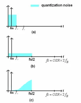
Oversampling technique is widely used to achieve high resolution in data converters. It is using a higher sampling rate than the Nyquist rate. The factor oversampling ratio (OSR) is defined as OSR= fs/ 2fB. Figure 2.1(a) and (b) are
output spectra of a Nyquist sampling, the noise power spreads over signal band,
B
f , which is half the sampling frequency, . The last term of Eq 2-1 shows
that an double increase in the OSR results in an increase in SNR by 3dB.
/ 2 N
f
SNRMAX =6.02N+1.76 10 log(+ OSR) (dB) . (2-1)
2.2 Noise shaping
Though oversampling is a very simple way to improve SNR, it is not very practical to obtain very high resolution such as 16-20bits. In delta-sigma modulation (DSM), noise shaping is employed to relax OSR or, in other words, obtain higher SNR. The noise shaping property of the delta-sigma modulator can suppress the in-band quantization noise as depicted in Fig 2.1 (c).
Figure 2.1 Spectra of (a) a Nyquist sampling (b) an oversampling, and (c) an oversampling with noise shaping
A linear model of a noise-shaped delta-sigma modulator is shown in Figure 2.2.
Figure 2.2 Linear model of the modulator
The ouput in z-domain can be expressed as:
where ( ) ( ) 1 ( H z STF z H z = + ) . (2-3) 1 ( ) 1 ( NTF z H z = + ) (2-4)
The STF(z) is the input signal transfer function and NTF(z) is the noise transfer function. The quantization noise is indicated by E(z). The loop filter transfer function, H(z) of the first-order DSM must be a highpass function. Beacause the zeros of NTF(z) are equal the poles of H(z), we can get
1 1 ( ) 1 Z H z Z − − =
− . Therefore, The Eq 2-2 can
be rewritten as :
1 1
( )
( ) (1
) ( )
Y z
=
z U z
−+ −
z
−E z
(2-5)The quantization noise is shaped by a first-order differentiator. The quantization is shaped by a first-order differentiator. That results in reduced noise power in the signal band,
f
B, and increased noise power out of the signal band. Figure 2.3 shows thegeneral shape of zero-order, first-order, and second-order noise-shaping curves. The noise power over the band of interest decreases as the noise-shaping order increases. However, there are some issues about increase of out-of-band noise and stability for the higher-order modulators.
2.3 Comparison of One-bit and Multi-bit implementations
The comparison of one-bit and multibit modulators is based on oversampling ratio, linearity, stability, and out-of-band quantization noise. The main advantage of one-bit modulator is inherently linear since it only need to produce two output levels and two points can define a straight line. However, the one-bit modulator with higher-order is easy to become unstable. A stable modulator is defined as one in which the input to the quantizer remains bounded and the quantization does not become overloaded. An overloaded quantizer means its input signal is over the quantizer’s normal range. It causes the quantization error to be greater than ±Δ/2. Another disadvantage of one-bit modulator is to result in a large amount of out-of-band quantization noise, which must be significantly reduced by the analog circuit. Such a task requires relatively high-order analog filtering. It increases the difficulty in designing the analog filtering circuit.
A multibit modulator can provide the improvement in SNR. From the first term of formula (2-1), SNR increases 6 dB with increasing one bit in the quantizer output. Therefore, a multibit modulator of a given order can achieve the target of dynamic range with less oversampling ratio than a one-bit modulator of the same order. In the application of higher-order modulators, a multibit modulator is also more stable than a one-bit modulator [2]. Additionally, the use of the multibit modulator can significantly reduce the large amount of out-of-band quantization noise and tolerate relaxed out-of-band filter specifications, but it must take care to ensure the multibit output of the modulator remains linear. The linearity of the multi-level output is limited by the mismatches in the components which are used to generate the analog levels. The diagram of step mismatches in the D/A converter is shown in Figure 2.4.
Figure 2.4 Illustration of step mismatch in the D/A converter
These step mismatches caused by component mismatches result in the distortion over the signal band, and then reduce the obtained SNDR (signal-to-noise plus distortion ratio). In order to solve the mismatch problem, various linearization techniques have been proposed, such as trimming and dynamic element matching (DEM). The trimming technique is practical for a D/A converter to enhance the matching property of identical components. It does not require extra circuits to reduce mismatch effect if each component is trimmed individually. However, trimming technique is expensive, time-consuming, and not a one-time process since device aging and temperature variation occurring in the lifetime of a D/A converter reduce the effect of compensating mismatches. The algorithm of DEM will be discussed in the following section.
2.4 Oversampling delta-sigma DACs
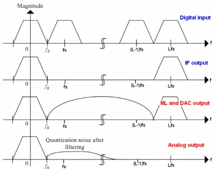
Delta-sigma data converters employ noise shaping and oversampling to achieve a wide dynamic range in the band-of-interest. It is extremely suitable for the audio application. Figure 2.5 shows its block diagram. The input signal is an N-bit sampled data with sampling frequency fs, which is often slightly larger than Nyquist rate. By passing through an interpolation filter(IF), its sampling frequency is increased to Lfs, and the images introduced by oversampling are removed. The output of the interpolation filter then feeds into the noise-shaping loop (NL) to M-bit output (M is much smaller than N ). These truncated bits then converted to the analog signal by an internal M-bit DAC. The quantization noise brought by the noise shaping process (most of the noise power is out of the interested signal band) is filtered by the following lowpass filter and the smoothed analog signal output results.
Figure 2.5 Block diagram of a delta-sigma DAC.
The sources of error in the delta-sigma DAC are the device mismatch which causes harmonic distortion, rather than component noise, device nonlinearities, clock jitter sensitivity and inband quantization error from the delta-sigma modulator.
Figure 2.6 Frequency spectra at different points of the delta-sigma DAC
A widely used structure for the M-bit internal DAC in the delta-sigma DAC is a so called unit-element DAC which is built from unit elements such as capacitors in a switched-capacitor circuit or current sources in a current-steering DAC. An advantage of such a DAC is that there are no glitches at its output [3]. Figure 2.7 shows the diagram of the unit-element DAC.
Chapter 3
Implementation of the Digital circuits in
ΔΣ DAC design
3.1 Interpolation filter design
3.1.1 1bit to 24bit converter
In order to save the chip’s pin count, the 1bit serial input data is converted into 24bit parallel output data for the signal processing performed in interpolation filter.
3.1.2 Principle of interpolation filter design
Figure 3.1 Block diagram of interpolation filter
The interpolation filter used in the delta sigma DAC is built by an upsampler and a lowpass filter as shown in Figure 3.1. The digital input signal x(n) is upsampled to u(n) by an oversampling ratio L. If the sampling rate of x(n) is a Nyquist rate fs, the
sampling rate of u(n) will be L fs. The Figure 3.2 shows the detail about how to
Figure 3.2 Interpolator’s spectrum
For example of oversampling ratio L , the input signal x(n) is converted into u(n) by inserting L-1 zero-valued samples between two consecutive samples of the input sequence x(n). The graph of Figure 3.2(a)(b) show the difference between x(n) and u(n). A low-pass filter h(n) is necessary to filter out the undesired image signal shown in the graph of Figure 3.2(c).
The anti-image filter is used to remove undesired images signal which replace the inserted zero value samples with proper values in time domain. The strict requirements on the linear phase characteristics in audio applications mandate the use of a finite impulse response (FIR) filter, rather than an infinite impulse response (IIR) filter. However, high order is necessary for a sharp cutoff FIR filter. Equation 3-1 gives the transfer function of typical FIR filter.
1 0 ( ) N ( ) n, n H z h n z − − = =
∑
h n( )real. (3-1) Here h(n) is the impulse response.Figure 3.3 FIR structure
3.1.3 Implementation of interpolation filter
Half-band lowpass filter (HBF) is hardware efficient in reducing the circuit complexity in the design of a sharp cutoff FIR filter. Its coefficients are symmetric with respect to the center tap, and around 50 percent are zeros [4], which allows the reduction by half of the required multiplication. The ripple in passband and
attenuation in stopband should be also properly set to avoid a huge computation and complex hardware.
Figure 3.4 Implemented interpolator
Using a single upsampler and a single lowpass filter often leads to the high computation complexity [4]. An efficient realization of the interpolation filter was realized with as a cascade of several stages, to avoid the high computation complexity. Figure 3.4 shows the designed interpolator. The first half-band FIR filter (HBF1) is the most complex one to be designed (55-tap) since the transition band for this filter is often very small. The second half-band FIR filter (HBF2), larger transition bands
make their order much smaller (11-tap). Each HBF coefficient was quantized to the sum of a few integer powers of two, and represented by a canonic signed digit (CSD). The CSD allows encoding a binary number such that it contains the minimum possible number of non-zero bits [5]. The complex multiplication with filter coefficient is thus replaced with a few shift-and-add operations without multiplier. Finally, the last stage of the interpolation filter is often implemented by using a digital sinc filter whose transfer function is given by [6].
( ) (1 1 1) 1 L K z H z L z − − − = − (3-2)
Where L is the interpolation factor
Figure 3.5 shows the architecture of implemented second half-band FIR filter [7].
Figure 3.5 Second half-band FIR filter
Figure 3.6 Frequency responses of HBF1 and HBF2
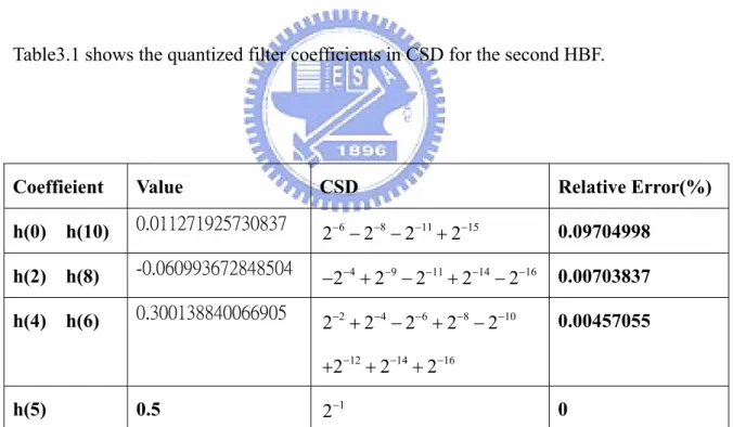
Table3.1 shows the quantized filter coefficients in CSD for the second HBF.
Coeffieient Value CSD Relative Error(%)
h(0) h(10) 0.011271925730837 2−6−2−8−2−11+2−15 0.09704998 h(2) h(8) -0.060993672848504 −2−4+2−9−2−11+2−14−2−16 0.00703837 h(4) h(6) 0.300138840066905 2−2+2−4−2−6+2−8−2−10 12 14 16 2− 2− 2− + + + 0.00457055 h(5) 0.5 2−1 0
Figure 3.7 shows the architecture of implemented sinc filter.
Figure 3.7 Implemented sinc filter
Figure 3.8 shows the frequency response of sinc filter.
Figure 3.9 shows the frequency response of interpolation filter after synthesis.
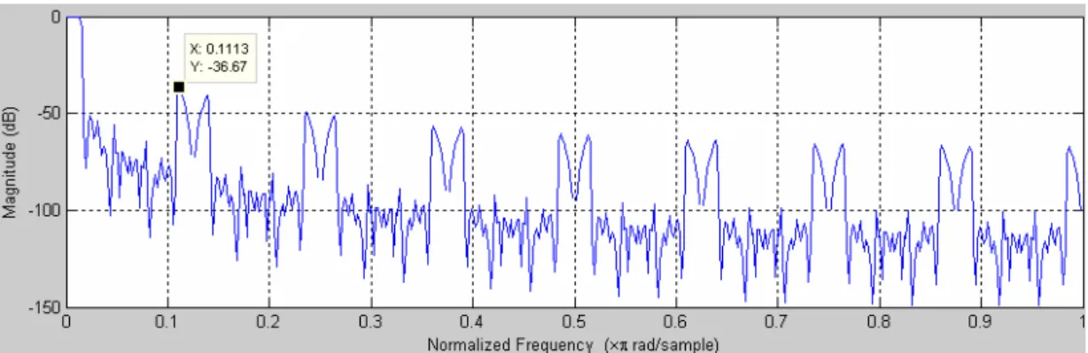
Figure 3.9 Frequency response of interpolation filter after synthesis
The interpolation filter is composed of two cascaded half-band FIR filters, followed by a digital sinc filter. It interpolates by the oversampling ratio (OSR=64), and achieves more than 36.67dB attenuation in the stopband and less than
ripple in the passband. The first two HBFs increase the OSR to 4, and the last sinc filter further increases the OSR by 16 times, to provide the overall OSR of 64. The orders of the two half-band FIR filter stages are 54 and 10. Thus, the numbers of realized distinct nonzero filter coefficients for these filters are 15 and 4.
0.03dB ±
3.2 Delta sigma modulator design
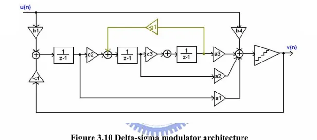
At the output of the interpolation filter, a delta-sigma modulator with third-order, CIFF (cascaded integrated feedforward) structure is shown in Figure 3.10 [6]. For accumulators in the CIFF structure, less bits are required to achieve the desired SQNR, because it only processes the errors between the input and the output. It is this
property that makes it less susceptible to coefficients truncation than that of the competing architectures.
Figure 3.10 Delta-sigma modulator architecture
Table 3.2 Modulator specifications
Parameter Value Input sampling rate 2.8224MHz
Signal bandwidth 20kHz Signal-to-noise ratio 120dB Modulator sampling rate 2.8224MHz Internal DAC levels 15
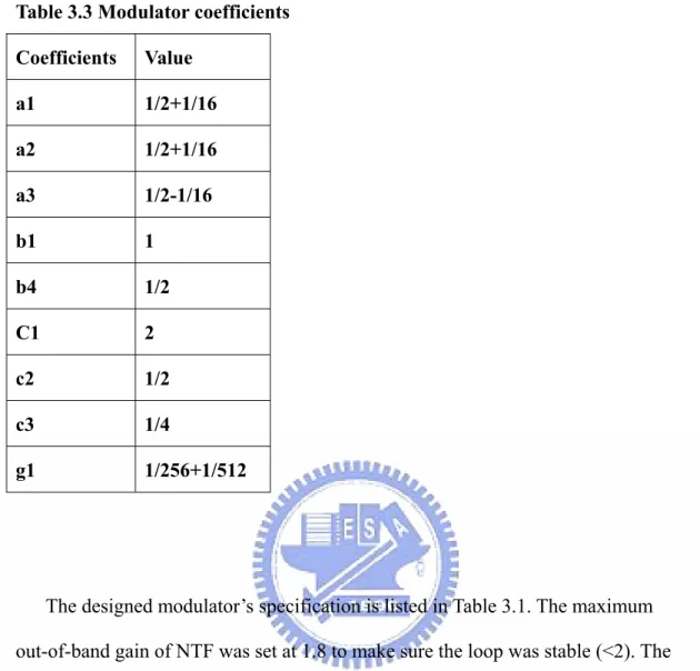
Table 3.3 Modulator coefficients Coefficients Value a1 1/2+1/16 a2 1/2+1/16 a3 1/2-1/16 b1 1 b4 1/2 C1 2 c2 1/2 c3 1/4 g1 1/256+1/512
The designed modulator’s specification is listed in Table 3.1. The maximum out-of-band gain of NTF was set at 1.8 to make sure the loop was stable (<2). The coefficients for the modulator were obtained by using delta-sigma toolbox [8] and are given in Table 3.2. The local feedback path (-g1) minimizes the in-band quantization noise in the modulator loop by placing two complex-conjugate zeros close to the edge of the signal band.
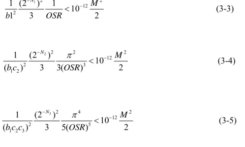
If , , are required to quantize the first, second, and third accumulator in the modulator loop, for a desired SNR better than 120dB caused by the finite word length of the accumulator and a full-scale sine wave with power of , , and are given by
1 N N2 N3 2/ 2 M N1 N2 3 N
1 2 2 12 2 1 (2 ) 1 10 1 3 2 N M b OSR − − < (3-3) 2 2 2 12 2 3 1 (2 ) 10 ( ) 3 3( ) 2 N 2 1 2 M b c OSR π − − < (3-4) 3 2 4 12 2 5 1 2 3 1 (2 ) 10 ( ) 3 5( ) 2 N 2 M b c c OSR π − − < (3-5) Solving eq (3-3), (3-4) (3-5) gives N1=12.732, N2 =8.5912, N3 =5.8742. [6]
Therefore, it is required to use 13, 9, 6 bits for the first, second, and third accumulator in the modulator. The resulting output waveform and spectrum of the delta-sigma modulator are shown in Figure 3.11 and Figure 3.12 respectively. The out-of-band spectrum is shown in Figure 3.13. As expected in delta-sigma modulator, a significant out-of-band noise is presented.
Figure 3.12 Output spectrum of the modulator
Figure 3.13 out-of-band spectrum of the modulator
The use of the multibit quantizer can also make the structure of the delta-sigma modulator more stable. However, the multilevel output requires using a number of unitary components at the digital-to-analog interface (i.e. capacitors), which is equal to the number of the quantizer output levels. The natural mismatches between the analog devices cause signal distortion. This problem can be solved by implementing dynamic element matching (DEM) at the digital-to-analog interface.
3.3 Dynamic Element Matching
A dynamic element matching (DEM) algorithm is to execute the randomized selection of the analog elements [9], [10]. It can avoid performance loss in terms of SNR and THD (total harmonic distortion) due to the mismatches between the capacitors, which is used in the input structure of the reconstruction filter. The noise due to distortion may be translated to white noise or shaped in spectrum depending on the used algorithms. For example, it may be a highpass characteristic. The randomized selecting process is realized in two stages, which are thermometer encoder and DWA (data weighted averaging) encoder [11]. They are shown in Figure 3.14. The 4-bit signal of the delta-sigma modulator output is translated into 15-bit signal by a thermometer encoder. Then this 15-bit signal is randomized by a DWA encoder.
Figure 3.14 The implementation of DEM process
3.3.1 Thermometer code encoder
The operation of thermometer encoder is to convert binary into thermometer code, with the lower ranks producing all ones, and the higher ranks producing all zeros. Then how many capacitors of the digital-to-analog interface must be charged depends on the thermometer code. This thermometer encoder is used to transfer the four signed bits of the delta-sigma modulator output signal. The four signed bits means the levels
Quantizer levels
Logic word or Number
of selected capacitors
Thermometer word
+7 15
111111111111111
+6 14
011111111111111
… … …
1 9
000000111111111
0 8
000000011111111
-1 7
000000001111111
… … …
-7 1
000000000000001
-8 0
000000000000000
Table 3.4 Operation of thermometer encoder
Note that no charge has to be injected in the analog reconstruction filter when the 0 logic level is chosen, so no input capacitors are selected.
3.3.2 DWA (data weighted averaging) circuit
The DWA algorithm uses all the internal DAC components of the analog reconstruction filter at the maximum possible rate while ensuring that each component is used the same number of times. This is realized by selecting components sequentially from an array, and then beginning with the next available unused component. Figure 3.15 illustrates the concept for a 3-bit DAC with an input sequence of 2, 4, 7, and 5. A 3-bit DAC can be translated into 7-bit thermometer code and
implemented by seven equally weighted elements. The first two elements of the DAC are selected when the input sequence, 2(1100000), is applied. The next four elements of the DAC are selected when the input sequence, 4(0011110), is applied. If the input sequence, 7(1111111), is applied, all elements of the DAC are selected. When the next input sequence, 5(1111001), is applied, the first four and the last one are selected. The component selection will continue in this manner sequentially as the input data is applied.
Figure 3.15 DWA operation
As described above, the element averaging is controlled entirely by the input data sequence. Thus, we can refer it to data weighted averaging (DWA) dynamic element matching. This element selection process can use all elements at the maximum possible rate, which ensures that the mismatch errors between components will sum to zero quickly, moving distortion to high frequencies. Another consequence of the cyclic sequencing is that no element of the DAC is selected with an inordinate numbers of times, even in a short time interval. A 15-bit internal DAC is adopted for this design. The input data is 15-bit thermometer code translated from the 4-bit data of the delta-sigma modulator output. The components of the DAC are selected according
Chapter 4
Implementation of the Analog circuits in
ΔΣ DAC design
4.1 DAC circuits
The block diagram of the analog part circuit is shown in Fig 4.1, which consists of internal DAC and post filter. The function of the internal DAC is converting digital signal input to analog signal output. And the function of the analog post filter is to smooth the digital signal and to reject the out-of-band noise, without compromising the signal purity achieved with the previous digital processing.
Fig 4.1 Block diagram of analog part circuit
The major concern in analog design is the minimization of power consumption and area size, while achieving the required DR (dynamic range) and SNRout
(out-of-band SNR). These two parameters refer to different aspects. The DR refers to the noise located in the signal band and is dominated by the 1/f and thermal noise of the analog part. The SNRout refers to the residual noise out of the signal band and is
dominated by the quantization noise, which depends on the amount of filtering section implemented in the analog part. The two parameters are in tradeoff: a larger amount of out-of-band filtering requires a larger analog filtering section and this causes higher
in-band noise, which reduce the DR. For the minimization of the power consumption and area size in addition to the low noise requirement, we realize the analog post filter with less operational amplifiers.[12]
4.1.1 Conventional Switched-Capacitor DAC
Figure 4.2 is a circuit diagram of a conventional switched-capacitor D/A converter. [13] The switched-capacitor D/A converter includes an operational amplifier. This amplifier is coupled to have a voltage follower function such that an output terminal of the amplifier is connected to an inverting input terminal. During φ phase, 1 switches S1 and S2 enter a closed state and the capacitor Cin is discharged by connecting to the ground. During φ phase, the switches S1 and S2 enter an open 2 state. At the same time, due to the operation of the switch S3, and depending on the polarity of the digital data. The output is charged.
Typically, a parasitic capacitance Cp is present at non-inverting input of amplifier. Parasitic capacitance is inherent in the manufacture and operation of the switching node. As a result, parasitic capacitance Cp will cause a large error to DAC’s output.
In order to solve the problems arising in figure 4.2, a switch capacitor D/A converter as shown in fig 4.3 may be used [13]. During the sample phase φ , 1 capacitors sample the data of the digital output. Shorting the input and output terminal causes the electric charge on the feedback capacitor Chold becomes zero. During integrating phase
in
C
2
φ , the output is charged. Since the inverting input terminal is always in the virtually grounded condition, the charge stored in the parasitic
capacitor when φ is at the high level is equal to that stored in the parasitic capacitor 1
when φ is at the high level. The overall result is there is no parasitic capacitance 2 added to the inverting input. However, this type of SCDAC has unacceptably large power consumption because the amount of charge to be supplied by the opamp.
4.1.2 SC DAC using Direct-Charge-Transfer technique
In a conventional SC DAC, an increase of capacitor size in attempt to reduce kT/C noise requires a corresponding increase of power consumption. Using the DCT-SC (direct charge transfer switched-capacitor) technique makes its power dissipation less dependent on capacitor size [14]. This technique was originally proposed to realize a robust unity gain amplifier and was later adopted to prevent the problem of opamp slew limiting at the switched-capacitor to continuous-time interface in the analog reconstruction filter of a 1-bit DAC. Slew limiting in the opamp results in a spike in stair step waveform, which causes distortion when it is filtered in continuous-time. The concept of an internal DAC with DCT-SC technique is shown in Figure 4.4.
Figure 4.4 Concept of the DCT-SC technique [14]
During the sample phase φ , capacitors 1 sample the data of the digital output.
During the hold phase
in
C
2
φ , the top of is connected to the inverting input of the opamp and the bottom plates are all connected to the opamp output. By this operation, the charge sampled at
in
C
1
φ will be distributed averagely by direct charge transfer among the capacitors at φ . Therefore, the analog output level is generated without 2
the support of the opamp. Since the input capacitor Cin directly transmits the charge to
the integrating capacitor Chold, the opamp does not need to provide charging current
for the capacitors.
The use of DCT technique makes the slew component of power consumption negligible and independent of capacitor size, because the power required charging the bottom plate parasitic capacitance mostly determines the power consumption. Hence this reason allows use of larger sampling capacitors for resisting noise with small increase of power consumption. At the discrete-to-continuous-time interface, any nonlinearity of the analog output waveform will be converted into noise or distortion in the following lowpass filter. By use of SC technique, clock jitter does not affect the analog levels of the discrete-time sampled points if the settling is adequate. However, when observed in continuous-time, clock jitter appears as a random signal which causes the stair step waveform of the output. The output signal includes high frequency quantization noise, which will be modulated into the signal band. Fortunately, the integrating capacitor Chold provides a first-order lowpass characteristic
with a cutoff frequency about 170 kHz in addition to the DAC function. This reduces the high frequency quantization noise and the noise modulated back to the signal band.
4.1.3 Other examples of DAC circuits
An example of 5-bit SC DAC with hybrid post filter is shown in Fig 4.5 [15]. Each capacitor array consists of 31 unit capacitors, to . During the sampling phase
1
C C31 1
φ , they sample the data which comes from DWA (digital) output. During the integrate phase φ , all capacitors are connected in parallel between the summing 2
node and opamp output. The output level is generated passively by distributing the charge in the feedback path. Each half of the differential circuit has two capacitor arrays. One is controlled by the DWA output data, and the other by data delayed one cycle. This realizes the two-tap FIR filter with 1 z+ −1 transfer function. The feedback
capacitor provides a first-order LPF function. The cut-off frequency is determined by the ratio between and
FB
C
FB
Another analog part circuit for ΔΣDAC, described in [16], used a 13-level truncation. Its Switched-Capacitor Filter was a third-order Chebyshev filter. This saved one amplifier. It is shown in Fig 4.6 as a single-ended circuit (the actual implementation was fully differential). During the sampling phase, an array of twelve unitary capacitors is switched to VDD or ground according to the related code coming from the ΔΣ modulator, while during the integration phase, all the capacitors are connected in parallel between the first opamp input node and the SC filter output. Third-order SC Chebyshev filter was used to strongly reduce the out-of-band noise and a 1st-order continuous time filter was then followed.
Fig 4.6 Third-order SC reconstruction filter [16]
Third example, an audio DAC is realized by using an SC array to transfer the sampled charges directly into the integrated headphone driver [17]. Thus, the DAC and the driver can all be combined, and need only one opamp. Fig 4.7(a) shows the second-order Sallen-key filter which is commonly used as the reconstruction filter in
audio delta-sigma DACs. The DAC output is applied to this filter to remove out-of-band noise. In this system, the input resistor R1 is replaced by a SC structure
as shown in Fig 4.7(b). By digitally controlling the SC branch, it can be used to perform the DAC function, saving hardware.
Fig 4.7 DAC stages (a) Conventional Sallen-Key filter (b) SC realization (c) Correction stage [17]
Fig 4.8 Gain-corrected DAC [17]
A problem with this new configuration is that the dc gain of the DAC is poorly controlled. The transfer function of the traditional Sallen-Key filter is given by
2 1 2 2 3 1 2 2 3 2 3 1 1 / ( ) 2 ( / ) R R H s R R C C S R R R R R C S 1 − = ⋅ ⋅ + + + ⋅ ⋅ + (4-1)
The dc gain of the filter is thus given by the ratio of R2 and R1, which is well
controlled on chip. However, in the modified structure, the amplitude A of the filter output signal at dc is given by
2
2 rsc DAC/ 1
A= ⋅ ⋅n V ⋅R C⋅ T (4-2)
Here, is the reference voltage sampled by the SC array, n is the number of the unit elements in the SC array and is the clock period in the DAC. Eq (4.4) shows that amplitude A depends on the time constant
rsc
V
1
T
2 DAC
R C⋅ which is poorly controlled on
chip. To control the amplitude A accurately, a gain correction stage was introduced, as shown in Fig 4.6(c). In steady stage, the dc currents entering nodes A and B through the resistive and SC branches equal zero. The output voltages are then given by
) 2/( ) ref r r V+ = +V ⋅T R C⋅ (4-3) 2/( ) ref r r V− = −V ⋅T R C⋅ (4-4)
Here, is the clock period in the correction circuit. This stage generates the reference voltage for the DAC output stage. Combing (4.4), (4.5) and (4.6) gives
2
T
2 1 2
2 rsc ( / ) ( / r) ( DAC/ r
A= ⋅ ⋅n V ⋅ T T ⋅ R R ⋅ C C (4-5)
Eq (4-5) shows the amplitude A now depends on ratios of R and C values, which can be accurately controlled with careful layout.
Finally, an analog section of the DAC, which includes a resistor-array DAC (R-DAC), a second-order Sallen-Key low-pass filter, and the headphone driver is shown in Fig 4.9. In the resistor-array DAC, all switches are connected either to the high reference voltage or the ground. This avoids the problems with floating switches. An analog first-order FIR filter is also integrated into this DAC ( is delayed by one clock cycle with respect to in Fig 4.8). This introduces a zero at one-half of the sampling frequency, and reduces the clock jitter sensitivity [18].
i
d
i
Fig 4.9 Resistor array DAC with first-order FIR filtering [18]
4-2 Low-voltage Circuit design issues
4-2.1 Floating Switch
Switches are affected by low supply voltage. Fig 4.10 shows the limitation on the operation of a floating switch in switched capacitor circuits. These limitations arise when the supply voltage is smaller than or equal to the sum of PMOS and NMOS threshold voltages (V |). If the power supply voltage, VDD is smaller then
( ), the switch will not be turned on even if the control signal voltage level of the NMOS is same as VDD or that of the PMOS is ground level. This is called the floating switch problem which is a serious concern in low-voltage switched-capacitor circuit design. The existing techniques that deal with this issue are discussed in the following section. | THN+ VTHP | | THN THP V + V
Fig 4.10 A SC integrator and the floating switch problem
4-2.2 Low-threshold Voltage Device
Lower threshold NMOS and PMOS transistors can be used at the expense of an extra mask layer for the CMOS process. It gives a simple and straightforward solution for the low-voltage SC circuit implementation, except for the extra cost of additional processing. However, the leakage current of MOS transistor with low threshold voltage limits the accuracy of charge transfer, and hence the effectiveness of this approach.
4-2.3 Clock voltage doubler
The clock voltage boosting technique increases the gate-source overdrive typically achieved by doubling the clock voltage applied to the gate of an NMOS floating switch. Fig 4.11 shows a clock boosting circuit proposed by Nakagome et al [19]. When the input signal is at VDD, capacitor C2 is charged to VDD by connecting the
phase, the output level of the boosted clock is lowered by turning off PMOS transistor M1 and turning on NMOS transistor M2. When the input signal is low, an inverted clock will pump the voltage at the top plate of to be almost 2VDD and PMOS device M1 will turn on to pass the boosted voltage to the gate of the floating switch MS. The peak voltage of the boosted clock signal is
2 C 2 2 , 2 HI p gate M C V VDD C C C = + + S (4-8)
Where Cp is the parasitic capacitance at the top plate of C2 and Cgate MS, is the
gate capacitance of the floating switch MS. However, this approach introduces severe reliability issues in fine-line CMOS technologies due to the gate-oxide stress and p-n junction problems.
4-2.4 Clock Bootstrapping
Clock bootstrapping technique [20] also enables a low-voltage switching operation using higher gate overdrive voltage. Linearity of the switch is also improved due to constant on-resistance resulting from constant . Fig 4.11 shows the basic concept of bootstrapped circuits. During
GS
V
1
φ state, the capacitor is precharged to VDD. It will ideally act as a floating battery to bootstrap the gate voltage during φ state. 2
Assuming that the input terminal of the sampling switch is source, the “on” resistance is given by 1 ( ) n ox DD tn Ron W C V V L μ = − (4-9)
Clearly, it is independent of input signal to reduce harmonic distortion. However, it requires separate bootstrapping circuits for each switch, resulting in more die area and power consumption.
Fig 4.12 (a) Clock bootstrapped circuit (b) phase φ (c) phase 1 φ 2
4-2.5 Switched-RC technique
The switched-RC technique was proposed in [21]. In this scheme, the floating switch is replaced directly by a resistor as shown in Fig 4.13.
Fig 4.13 (a) Switched-RC Integrator (b) phase φ (c) phase 1 φ 2
This greatly improves the sampling linearity without using the clock bootstrapping. The integrator works as following : during clock phaseφ1 , capacitor , samples the
input through resistor R1, and switch S2, during clock phase
S
C
2
φ , charges stored in capacitor , will be transferred to the integrating capacitor . During the integrating phase, the resistor R1 and switch S1 will form a resistor divider through which the input signal will have a leakage at node X given by
S C CF 1 ON X ON R V Vin R R = + (4-10)
1 S ON F ON C R Vin C R +R (4-11)
The ratio of RON and R1 can be sized carefully to give a small gain.
4-3 Class AB amplifiers
The headphone driver is a key part in the audio applications which may define the performance of the overall system. A driver is an amplifier which can drive a low resistance and large capacitance load and has a small quiescent current. There are many different drivers (Class A, Class B, Class AB and Class D) that are classified according to their output stages and shown in Fig 4.14.
Fig 4.14 ClassA, AB, B output stages
A Class-A stage is a stage in which the peak current swing never exceeds the DC biasing current. The average current is therefore the DC current. In a Class-B stage the DC biasing current is zero. Connecting these swings to the negative swings from another amplifier leads to discontinuities, which is called crossover distortion. Class-AB amplifiers are somewhere in between. The DC biasing current (or quiescent current) is small compared to the peak current swings. It is well-known for its good
efficiency and is used widely in audio application, it requires further off-chip filtering and has the IM signal around the switching frequency. Thus, it has greater noise as compared with the other amplifiers.
To deliver power to small resistors or large capacitors cannot be achieved with conventional output stages. The output currents are too large. For this purpose we need to bias the output stages in Class-AB. They have small quiescent currents but can deliver very large currents to the load.
4-3.1 CMOS output stage
For a low-resistor load, a low output impedance is required. The source follower is the only simple transistor stage which provides this output resistance. However, its DC current handing is not sufficient. A source follower is shown in Fig 4.15, biased at 0.1mA. A low resistor of is connected to it. It is clear that the maximum output voltage swing can only be 5mV. For higher output voltages, we would need higher biasing currents as well. This would lead to an excessive power consumption. We now need a transistor circuit which can deliver large currents only when needed, but with a low quiescent biasing current to lower the power consumption as much as possible.
Fig 4.15 CMOS output stage problem
A possible solution is to have two source followers, Source to Source, as shown in Fig 4.16 (b). The current out of this stage can again be very large, depending on the transistor size. The PMOS can now be driven as hard as the NMOS. The main disadvantage of this double source follower is that the output swing can only reach the supply voltage within one . Also, the output voltage can never be lower than
. For large supply voltages, there is no problem but for supply voltages of a few Volts, this is not acceptable. This is why most Class-AB output stages for low supply voltages have two output transistors Drain-to-Drain.
GSn
V
GSp
V
The basic requirement of class-AB stage is described as following. The first requirement is obviously that rail-to-rail swings are possible. The second one has indeed to do accurate control of quiescent current I , it must be low and independent Q
of supply voltage. Third, drive capability (defined as IMAX /I ) must be as large as Q
possible. The last specification has to do with complexity. Class-AB amplifiers are the most complicated DC-coupled amplifiers. Some simplicity is still welcome !
4-3.2 Cross-Coupled quads
A better class-AB amplifier is obtained by cross-coupling the input devices. In this way, a complementary differential pair can be constructed with an expanding characteristic. Figure 4.17 shows a simplified schematic of a cross-coupled class-AB amplifier which is proposed by Castello [22]. This circuit is perfectly symmetric. For zero applied differential input signal, the two matched current sources I uniquely define the circuit quiescent current level. In fact, if for simplicity it is assumed that the four NMOS input devices are identical, and the same is true for the four PMOS devices, then I1 =I2 = I. Furthermore since all current mirrors have a gain of 1, the
quiescent current in the output branches is also equal to I. It follows, therefore that the quiescent power consumption in the circuit is precisely controlled by the two matched current source in the input stage. The dynamic behavior of the circuit is described as following.
Fig 4.17 Castello’s Cross-coupled Class-AB Amplifier [22]
In response to a large positive differential input signal, current I1 goes practically
to zero. As a consequence, half of the devices in the circuit become cut off. Current
2
I , on the other hand, increases to a peak value which, in principle, is only limited
by the value of the input voltage applied. The same current is mirrored to the outputs and can quickly charge and discharge the load capacitance. In simply, transistor M1-M4 form a cross-coupled input stage which split the input signal into two paths and provide the class-AB operation. M5-M8 and the two current sources (I) perform the level shifting and provide proper bias for the cross-coupled input devices. Transistors M9-M20 form four current mirrors which duplicate the currents of the input devices with a 1:1 ratio.
The same cross-coupling which is shown in Fig 4.18 is now used here in the output stage [23]. The cross-coupled pairs M13, M14, and M15, M16 provide an inherently symmetrical drive to the output transistors. The quiescent output current is a simple function of the current flowing through the level-shift transistors M17-M20,
M16. This current is multiplied by a factor of 10 in the output current mirrors M21-M24.
Fig 4.18 Fischer’s Amplifier output stage [23]
The entire amplifier schematic is shown in Fig 4.19 [23]. A folded cascade input stage has been modified by adding an additional input transistor pair in order to create a symmetrical common-mode range. Assuming for the moment that node B is to be tied to ground and no input voltage is applied when the amplifier is in closed loop, symmetry dictates that node A will also be near ground. In this condition, the
drain-gate connection of transistors M17 and M18 has less than 0.5V overhead before transistors M8 and M10 begin to leave the saturation region. This small voltage swing is not enough to generate the large output currents required and also maintain a good low-level bias. Therefore a matched load inverter M25-M28 is inserted between node A and node B. This inverting buffer provide a gain of -1 at the expense of only four transistors and effectively doubles the voltage drive to the cross-coupled pairs, thereby maximizing the achievable current range.
Fig 4.19 Entire Fischer’s Amplifier schematic [23]
4-3.3 Adaptive biasing
Cross-coupled quads are a useful principle for generating expanding differential currents. It is not the only one however. Positive feedback can be used as well. Adaptive biasing is actually used. An adaptive biasing amplifier adapts its biasing to be able to provide larger output currents. The amplifier shown in Fig 4.20 is a symmetrical amplifier, which is single ended. Two times two current mirrors are added, i.e. with transistors M11/M12 and M13/M14. Without these transistors the maximum output current would be limited toBIP.
In order to increase this maximum current, biasing currentIPmust be made larger
for larger input voltages. This biasing current is adapted to the input signal level. This is why it is in parallel with two more current mirrors through transistors M18 and M19. Let us follow the path to transistor M19.
Fig 4.20 Adaptive Biasing Amplifier [24]
Transistor M19 forms a current mirror (with current factor A) with M20. This latter transistor take the difference in currentI1−I2, which are proportional to the
currents in the input stage. The larger of these two currents wins. IfI1 is larger thanI2
then AI1current is added toIP, increasing the total biasing current of the first stage,
and also increasing the maximum output current. If, however,I2 is larger thanI1, then
it is mirrored by M17/M18, also multiplied by A and also added toIP. This total
biasing current increases in either direction. The amount of increase depends on current factor A. A disadvantage of this amplifier is that transistors M11-14 are added on the node where the non-dominant pole is formed. They will therefore slow down the amplifier. (dominant pole is formed by the high output impedance and a load capacitor, and the second pole is formed by the transconductance of the load transistors of the input stage and the internal capacitors)
4-3.4
IQcontrol with translinear circuits
A Class-AB output stage can also be biased by translinear circuits. A translinear loop is a circuit which provides a linear relationship by use of nonlinear circuits. The simplest example is a current mirror. Both transistors have a nonlinear current-voltage relationship and yet the current gain is perfectly linear. The voltage between the two transistors is heavily distorted though.
loop is formed by transistors MA2/MA4 and MA9/MA10. Their sum of ’s is equal (Eq 4.5). The currents through MA9-MA10 are set by a DC current source (which is about
GS
V
4 Aμ in this example). The current through MA4 is also set by the DC current of the preceding stage (which is also about 4 Aμ in this example). Only the current through the large output transistor MA2 is not known.
2 4 9 GS GS GS GS V +V =V +V 10 (4-12) ' 1 ( )( ) 2 DS p GS TH W I k V V L = − 2 (4-13) Æ ' 2 ( ) DS GS TH p I V V W k L − = (4-14)
Combine (4-12) and (4-14). All parametersVTH,kp'and constant cancel out.
2 4 9 2 4 9 ( ) ( ) ( ) ( ) DS DS DS DS I I I I W W W W L L L L + = + 10 10 (4-15)
Table 4-1 Amplifier device size Device Size( mμ )
MA2 17 160 / 2.4×
MA4 2 64 / 4×
MA9 64 / 4
MA10 64 / 4
As a result, we obtain an expression linking in Table 4-1.
4 ( )W 2( )W L = L 9 and ( )2 70.8( ) W L = L 9 W (4-16) 2 9 4 9 9 9 2 9 4 9 9 9 1 2 2 2 ( ) ( ) ( ) ( ) 2( ) ( ) DS DS DS DS DS DS I I I I I I W W W W W W L L L L L L = − = − = (2− ) (4-17) 2 2 2 9 9 ( ) 1 (2 ) 118 2 ( ) DS DS W I L W I L ∴ = − = (4-18)
)
through transistor MA9. It is now well defined. It is independent of the supply voltage. The current through MA9/MA10 comes from a DC biasing current mirror. The DC current through MA4 comes from the PMOS differential current amplifier M11-M14 at the end of the NMOS first stage. This current flows through the NMOS differential current amplifier M5-M8 at the end of the PMOS first stage.
Complementary output devices MA1 and MA2 are driven by complementary common-gate level shifters MA3 and MA4. During quiescent operation, both MA3 and MA4 are biased into a conducting state. The gate-to-source bias voltages of the output transistors are kept low to minimize quiescent power consumption. The exact bias levels are controlled by the reference voltages and . During a negative slewing period, the gate voltage of MA1 will be pulled high. Fixed gate potential will cause MA3 to cutoff. MA4 will carry the full bias current, driving its source and the gate of MA2 high, turning off MA2. Under the condition of strong sourcing, MA2 will be turned on, symmetrically repeating the above operation on the other side of the circuit. Ultimately the swing on the gate of MA1 (MA2) will reach a limit at GS V 1 B V VB2 2 B V (
2VDS SAT from the positive (negative) rail. This large drive swing to both
output devices allows driving heavy loads close to the rails. After the slewing period, as the input signal returns toward zero, both MA3 and MA4 will turn on again and the circuit quickly settles to a quiescent stage.
Fig 4.21 Wu’s Amplifier [25]
This input stage is an improvement over the input stage of Fisher as the common mode voltage moves from the positive to the negative rail, the stage goes through three modes. First the PMOS devices are cutoff, then both device pairs operate, and finally the NMOS devices cutoff, during this time the input stage transconductance changes by a factor of 2. This requires excessive frequency compensation to ensure stability at all input levels.
The NMOS pair MI1, MI2, is biased by a current source MP1 via MN3 and the current mirror MN1, MN2, when the PMOS pair is nonconducting. When the common mode input voltage is at least equal the reference voltage above . When the input CM voltage decreases through the reference voltage , the source current is gradually steered from the source of MN3 to the PMOS pair, removing current from the NMOS pair. Since the tranconductance if MOS’s are proportional to the square
r
V VTH
r
transconductance variation of PMOS and NMOS pairs will be improved from a factor of 2 to a factor of 2 compared to the original circuit of Fisher []. To make the top PMOS cascade stage work symmetrically with the bottom NMOS stage it is employed a floating current source. Current mirrors are formed by MB6, M10 and MB5, M9. Transistors MB7 and MB4 act as resistors. The bias currents for the upper and lower cascade stages M11, M13 and M7, M5 are thus set equal. With proper selection of the ratio between MB5, M9 and Mb6, M10, we may set the reference current while maintaining node A and node B at the same potential.
A similar translinear loop to set the quiescent current through the output devices is found in Fig 4.22 [26]. The opamp contains a rail-to-rail input stage, M1-M4, with a control by three-times current mirrors, M5-M10 and M29-M31, a summing circuit, M11-M18, and a class-AB output stage, M19-M26. The floating current source, M27-M28, biases the summing circuit and the class-AB control.
m
g
The rail-to-rail folded cascaded input stage can be biased either in weak or in strong inversion. If the input stage is biased in strong inversion, then the total is given by m g ( ) ( ) m p ox p p n ox n W g C I C L L μ μ = + n W I (4-19)
From Eq 4-19, the transconductance can be made constant by keeping the sum of the square roots of the tail currents of the complementary input pairs constant. This yields
2 p n ref
I + I = I (4-20)
Where it is assumed that the W over L ratios of the input transistors obey the condition ( ) ( ) p n p n W L W L μ μ = (4-21)
The of this input stage is regulated by means of two current switches, M5 and M8, and two current mirrors, M6-M7 and M9-M10, each with a gain of three. For the sake of simplicity, this current mirrors will be called three-times current mirrors, in the remaining part of this section. The sizes of the input transistors are chosen such that relation 4-21 is obeyed.
m
g
Fig 4.22 Hogervorst’s class-AB amplifier [26]
In the intermediate part of the common-mode input range both current switches are off. The result is that the complementary input pairs are biased with a current of . And thus the tail currents obey Eq 4-20, in this part of the common-mode input
![Figure 3.5 shows the architecture of implemented second half-band FIR filter [7].](https://thumb-ap.123doks.com/thumbv2/9libinfo/8470854.183536/25.892.136.768.440.893/figure-shows-architecture-implemented-second-half-band-filter.webp)