surface science
ELSEVIER Applied Surface Science 99 (1996) 237-243
Properties of radio frequency magnetron sputtered silicon dioxide
films
Wen-Fa Wu, Bi-Shiou Chiou
*Department of Electronics Engineering and Institute of Electronics, Nationul Chiao Tung University. Hsinchu, Taiwan, ROC Received 17 July 1995: accepted 3 January 1996
Abstract
The rf sputtering method, using Ar/O, mixture, was applied to fabricate silicon oxide films. The compressive internal stresses, resulted from thermal expansion mismatch, of films deposited on polycarbonate are larger than those of films deposited on glass substrates. Addition of oxygen to the sputtering ambient reduces both the film deposition rate and grain size. The adhesion of the SiO, film to the glass substrate are measured with pull-off test and/or scratch test. Films sputtered in the presence of oxygen are more wear-resistant than those without oxygen.
1. Introduction
Silicon dioxide (SiO,) films have found applica- tions in many areas, such as optics [l-3], electronics [4-61, tribology [7,8], etc. In silicon microelectron- ics, SiO, films are generally employed for diffusion masking and passivation or protection of silicon devices [4,5]. Many novel optical coatings utilizes SiO, films to obtain the desirable refractive index in multilayer optical devices as well as the tribological resistance of the SiO, films for the anti-wear coating [7,8]. The usual methods employed for forming SiO, films involve oxidation of silicon at elevated temper- atures (T > 900°C). However, the high temperature processing results in junction degradation [4]. There are many low temperature methods used in the preparation of SiO, films, such as evaporation [2,3], pyrolytic decomposition [9], plasma enhanced chemi-
* Corresponding author. Tel.: +886-35.715507/712121; fax: + 886-35-724361.
cal vapor deposition [4-71, and reactive sputtering 19,101. Rao and Mohan utilized SiO, as the starting materials for electron-beam evaporation and pre- pared a highly stoichiometric SiO, films 1111. Val- letta et al. reported the preparation of SiO, films by reactive sputtering in Ar/O, mixture. They found that the deposited films were extremely porous and contained large amounts of H,,O when the film deposition rates were above 250 A/min [lo].
In this study, SiO, films were prepared by radio- frequency (rf) magnetron sputtering. Magnetron sput- tering can deposit films over large areas at rates comparable to electron-beam evaporation without the degree of radiation heating typical of thermal source. It is considered to be one of the best methods for preparing optical films, such as In,O,:Sn [12-171. In this research, the SiO, films were sputtered in an Ar-0, atmosphere. The effect of Ar/O, ratio on the deposition rate, the film morphology, the optical properties, as well as the adhesion of SiO, films to the glass substrates are evaluated.
0169.4332/96/$15.00 Copyright 0 1996 Elsevier Science B.V. All rights reserved. PII SOl69-4332(96)00103-l
738 W.-F. Wu. B.-S. Chiou /Applied Surficcr Science YY (fYY661 237-243
2. Experimental details 200
SiO, films were prepared by using a commercial rf magnetron sputtering system (ION TECH, Eng- land). The sputtering target was a 1 inch hot-pressed SiO, ceramic (99.9% purity) supplied by Supercon- ductive Components, USA. The substrates employed were Coming 7059 glass, polycarbonate sheets and p-type Si (1001 wafers. The substrate was fixed directly above the target and a mechanical shutter was attached to the target. High purity Ar (99.999%) or Ar/O, gas mixture was introduced through a mass flow controller after the vacuum chamber was evacuated to about 2 X 10e6 Torr. The rf power (13.56 MHz) was introduced through an rf power supply (Rf Plasma Products, USA) with an automatic matching network which could be tuned for mini- mum reflected power. Before deposition, the target was usually presputtered for 20-30 min to remove any contaminants and eliminate any differential sput- tering effects.
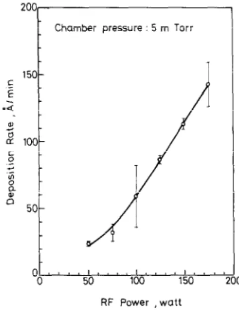
Fig. I. The deposition rate of SO2 films as a function of sputtering power.
Film thickness was measured with a stylus surface profiler. An X-ray diffractometer (XRD, Rigaku Dmax-B, Japan) was used to identify the crystalline phase of the film. The microstructure of the films was analyzed using a scanning electron microscope (SEM, Hitachi S-4000, Japan). The optical transmit- tance of the films were measured with an ultra-violet visible near-infrared spectrophotometer (Hitachi U- 3410, Japan) and a Fourier transform infrared spec- trophotometer (Bomen DA 3.002 FTS and MB 100 FT-IR, Canada).
ent scratches. Detailed morphologies of scratch chan- nels were viewed with an optical microscope.
3. Results and discussion
The adhesion strength of the coating was mea- sured by an adhesion pull tester (Sebastian Five Pull Tester, Quad Group, USA) and a scratching adhesion tester (CSEM Revettest, Switzerland). In the scratch- ing test a stylus is drawn over the sample surface under a continuously increasing normal force until the coating is detached. The normal force on the indenter causing coating detachment is called the critical load and it represents a comparative value of the coating adhesion. In the study, the loading speed and sample table speed are 100 N/min and 10 mm/min, respectively. The coating detachment was observed using acoustic emission detectors to mea- sure high frequency vibrations caused by coating detachment. The critical loads indicated were ob- tained by averaging the values of three to five differ-
Deposition rate is defined as film thickness di- vided by deposition time, and it is important in film thickness control, especially for precise multilayer coating. Fig. 1 shows the deposition rate of SiO, films as a function of sputtering power at a target- to-substrate distance of 5 cm and an argon pressure of 5 mTorr. The deposition rate increases with in-
20
.G - Sputtermg power : 100 W. E -
Fig. 1. The deposition rate of SiOz films on glass substrate as a function of oxygen percentage.
Chamber pressure : 5 m Torr
10
RF Power , watt
W.-F. Wu. B.-S. Chiou /Applied Surface Science 99 C lY96) 237-243 239
‘.‘... PC substrate
20- - SiO, film without crack __-_ Si02 f!lm wth crack 0 1 * I 1 1 . 1 500 1000 1500
1’
d
\ \
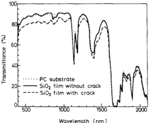
2ooo Wavelength (nm)Fig. 3. The spectral characteristics of SQ films on polycarbonate substrates.
creasing sputtering power. The high deposition rate at large sputtering power is attributed to the high energy of the sputtered neutrals. The higher sputter- ing power causes an increase in the density and average energy of the sputtered neutrals, which must then be subjected to a larger number of collisions before they are thermalized [ 151.
Fig. 2 gives the deposition rate of SiO, films as a function of the oxygen percentage at a sputtering power Ff 100 W. The deposition rate decreases from
* 13 A/min to N 4 A/min as oxygen percentage from 0 to 20%. For SiO, films deposited on polycar- bonate substrates, cracks are found after specimens stored in the atmospheric environment for several hours or several weeks. It implies a release of resid- ual stress after room temperature storage. The stress S, accumulated in the film after deposition is
s,=E~(a,-cx,)(T,-7-,). (1)
where E,. is the Young’s modulus for the film, of and 01, are average thermal coefficients of the film
28, degree
Fig. 4. The typical X-ray diffraction patterns of the as-sputtered SiO, film on glass substrate.
and the substrate, respectively, TD is the film deposi- tion temperature and TM is the temperature during stress measurements, i.e., room temperature. The residual stress of the film is attributed to thermal expansion mismatch, CY f - a,. and a temperature
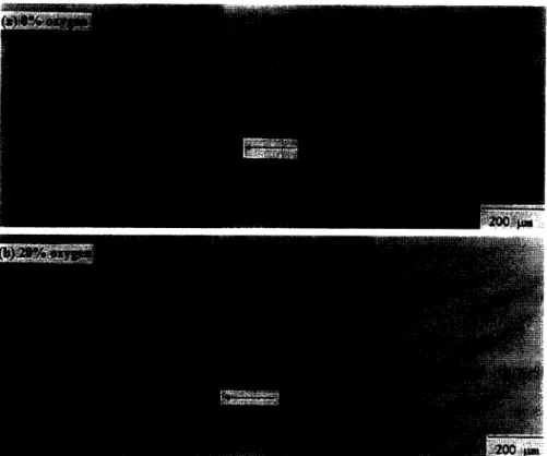
Fig. 5. SEM micrographs of SiO, films prepared at various oxygen percentages: (a) 0%. (b) 109’0, (c) 20%. The sputtering power is 100 W.
240 W.-F. Wu, B.-S. Chiou/Applied Surface Science 99 (19961237-243
change, TD - TM. The thermal expansion coeffi- cients of the SiO, film, Coming 7059 glass and PC substrate are 2 X 10m6/“C [18], 4.6 X 10e6/“C and 39 x 10_6/“C [19], respectively. The deposition temperature was N 90°C. Hence a compressive stress was built-up in the film and strain energy were accumulated. Cracks initiation and propagation would release the residual energy inside the films. Fig. 3 shows the spectral characteristics of the SiO, film with and without crack on polycarbonate substrates. An apparent reduction in the transmittance is ob- served for the cracked film. It is attributed to the increasing light scattering for the cracked film since cracks on the film increase the surface roughness of the film.
30
Wavenumber , cm-’
The as-deposited films are amorphous, as exhib- ited in the X-ray diffraction patterns shown in Fig. 4. The surface morphology of films prepared at various oxygen percentages are illustrated in Fig. 5. SiO, grains of the films are smaller than 20 nm. Films sputtered at higher oxygen content have smaller grain size.
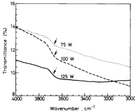
Fig. 7. The infrared spectra for SiOz films on silicon wafers prepared at various sputtering powers. Sputtering atmosphere: Ar. Arrows indicate the absorption band due to hydrogen bonded hydroxyl groups and absorbed water.
The Fourier-transform infrared spectroscopy is one of the best techniques for structural evaluation of silicon oxide films. Fig. 6 shows the infrared spectra in the region between 1400 cm-’ and 600 cm-’ for SiO, films prepared at various sputtering powers. It has been reported that the wave numbers correspond- ing to the Si-0 vibrational band are 968, 1035 and
1078 cm-’ for SiO, Si,O, and SiO,, respectively [20]. As shown in Fig. 6, the positions of the Si-0
vibrational band of rf sputtered SiO, films are 1080 f 5 and 840 cm- ‘. They agree well with the band positions of SiO, reported in the literature [9,10,20]. Fig. 7 shows the infrared spectra in the region be- tween 3000 cm-’ and 4000 cm-’ for SiO, films prepared at various sputtering powers. The intensity of the absorption band near 3650 cm-’ due to hydrogen bonded hydroxyl groups and adsorbed wa- ter is indicative of the quantity of surface hydroxyl groups and porosity of the oxides. As sputtering power increases, the intensity of the absorption band enhances. It implies the increase in the porosity of
glass substrate -..-..- 100 W ---- 125 W - 150 w Wavenumber , cm-’
tJ.
OO 1 400 1 a . 600 fi . a . ml 1 Wavelength (nm)Fig. 6. The infrared spectra for SiOz films on silicon wafers Fig. 8. Transmittance of SiO, films on glass substrates prepared at prepared at various sputtering powers. Sputtering atmosphere: Ar. various sputtering powers. Sputtering atmosphere: Ar.
W.-F. Wu, B.-S. Chiou/Applied Surface Science 99 (19%) 237-243 241
Wavelength (nm )
Fig. 9. Transmittance of SiO, films on glass substrates prepared at various oxygen percentages. Sputtering power: 100 W.
the film as films is deposited at high sputtering power.
Fig. 8 shows the spectral characteristics of SiO, films prepared at various sputtering powers. It can be seen in Fig. 8 that the transmittance of the film is high and all the films are free from absorption except oscillations due to interference effects, Fig. 9 shows the transmittance of SiO, films prepared at various oxygen percentages. Transmittance of the film is high and very close to that of the glass substrate. The variation of transmittance with wavelength appears to be similar for all films.
l5i .ur E w .u iii
a
Y
0 5 10 15 20 5 LOAD [N]Fig. 10. The acoustic emission curves for SiO, films prepared at various oxygen percentages.
that the bonding between the SiO, film and the glass substrate is excellent.
Table 1 summaries the results concerning the The scratch test is also employed to study the adhesion of SiO, films to glass substrates. As indi- adhesion of the film and substrate. The critical load cated in Table 1, a high pull-off strength ( > 500 measured by a scratch test technique can be thought kg/cm*> is obtained for films deposited on glass of as the adhesion strength of the film on the sub- substrates. Almost all the failures occurred within the strate when films are subjected to wearing and/or glass substrate and did not occur at the interface abrasion. Fig. 10 shows the acoustic emission curves between the film and the glass substrate. It implies for films prepared at various oxygen percentages.
ACOUSTIC EMISSION- LOAD GRAPH
(a) 0% oxygen
B
a
I I I I.s
ACOUSTIC EMISSION- LOAD GRAPH In5, (b) 20% oaygen
Table 1
Adhesion of SiO, films deposited on glass substrates
Sputtering atmosphere a 9O%Ar + lO%O, 9O%Ar + lO%O, 90BAr + 10%02 SO%Ar + 20%0, IOO%Ar
Sputtering power (W) 150 125 100 100 100
Pull-off strength (kg/cm*) 501 b 266 b 416 b 396 b 305 b
Critical load (N) - - - 8.0 f 2.0 5.9 + 0.9
a Chamber pressure is 6 mTorr. b Failure occurred within glass substrates.
242 W.-F. WK. B.-S. Ch IY96J 237-243
Fig. Il. The optical micrographs of the scratch channel for SiO, films prepared at various oxygen percentages.
The critical load, as summarized in Table 1, for films prepared at 0% and 20% oxygen are 5.9 k 0.9 N and 8.0 + 2.0 N, respectively. The film prepared at 20% oxygen appears to have a better scratch adhesion property than those prepared at 0% oxygen. Fig. 11 shows the corresponding scratch channel by the opti- cal microscope. The arrow indicates the scratch di- rection. A serious scratch damage is observed for film prepared at 0% oxygen, as observed in Fig. 11. Roughly semicircular arcs appear in front of the scratch channel, as shown in Fig. 11. The cracking is more intense and is coupled with a loss of adhesion at higher loads. However, the film is not removed as its coherence is high.
4. Conclusion
Silicon dioxide films were prepared by rf sputter- ing using Ar/O, mixture as sputtering gas. The deposition rate decreases with the increase of oxygen
percentage. Films sputtered at higher oxygen content have smaller grain size. The infrared spectra of the film confirm the presence of a stoichiometric SiO, film. However, the absorption band near 3650 cm- ’ suggests the existence of surface hydroxyl groups and porosity. The adhesion strength of SiO, film to the glass substrate is larger than the strength of the substrate after pull-off test. Films prepared at 20% oxygen appear to be more wear-resistant than those prepared without oxygen.
Acknowledgements
This work is supported by the Chung-Shan Insti- tute of Science and Technology (contract No. CS 83-0210-D-009-001) and partly supported by the Na- tional Science Council of Taiwan, ROC (contract No. NSC 82-04 17-E009-395).
W.-F. Wu. B.-S. Chiou/Applied Surface Science 99 (1996) 237-243 243
References
Ill H. Takahashi, H. Nagata, H. Kataoka and H. Takai. J. Appl. Phys. 75 (1994) 2667.
[2] E. Welsch, H.G. Walther, D. Schafer, R. Wolf and H. Miller. Thin Solid Films 156 (1988) 1.
[3] J. Stone and L.W. Stulz. Appl. Opt. 29 (1990) 583. [4] S. Robles. E. Yieh and B.C. Nguyen, J. Electrochem. Sot.
142 (1995) 580.
[5] H.O. Pierson, Handbook of Chemical Vapor Deposition: Principles. Technology and Applications (Noyes, New Jer- sey, 1992).
[6] R.K. Chanana, R. Dwivedi and S.K. Srivastava, Solid-State Electron. 36 (1993) 1021.
[7] W. Klug, R. Schneider and A. Ziiller, Proc. SPIE 1323 (1990) 88.
[8] J.D. Masso, Proc. SPIE 601 (1985) 60.
[9] W.A. Pliskin and H.S. Lehman, J. Electrochem. Sot. 112 (1965) 1013.
[lo] R.M. Valletta, J.A. Petri and J. Riseman, Electrochem. Tech- nol. 4 (1966) 402.
[l I] K.N. Rao and S. Mohan, Thin Solid Films 170 (1989) 179. [12] W.F. Wu and B.S. Chiou, Appl. Surf. Sci. 68 (1993) 497. [ 131 B.S. Chiou and S.T. Hsieh, Thin Solid Films 229 (1993) 146. [14] B.S. Chiou, ST. Hsieh and W.F. Wu, J. Am. Ceram. Sot. 77
(1994) 1740.
[15] W.F. Wu and B.S. Chiou, Thin Solid Films 247 (1994) 201. [16] B.S. Chiou. S.T. Hsieh and W.F. Wu, Appl. Surf. Sci. 74
(1994) 297.
[17] W.F. Wu. B.S. Chiou and S.T. Hsieh. Semicond. Sci. Tech- nol. 9 (1994) 1242.
[18] H. Sankur and W. Gunning, J. Appl. Phys. 66 (1989) 807. [19] D. Grzegorczyk and G. Feineman, Handbook of Plastics in
Electronics (Reston. Virginia, 1974).
[20] K. Narasimha Rao and S. Mohan, Thin Solid Films 170 (1989) 179.