Reliability Mechanisms of LTPS-TFT With HfO
2
Gate Dielectric: PBTI, NBTI, and Hot-Carrier Stress
Ming-Wen Ma, Chih-Yang Chen, Woei-Cherng Wu, Chun-Jung Su, Student Member, IEEE, Kuo-Hsing Kao,
Tien-Sheng Chao, Senior Member, IEEE, and Tan-Fu Lei, Member, IEEE
Abstract—In this paper, a comprehensive study of the
reliability mechanisms of high-performance low-temperature polycrystalline-Si thin-film transistor (LTPS-TFT) with HfO2
gate dielectric is reported for the first time. Various bias- and temperature-stress conditions, which correspond to positive-bias stress (PBS), positive-bias temperature instability (PBTI), negative-bias stress (NBS), negative-bias temperature instability (NBTI), and hot-carrier stress, are used to differentiate the distribution and mechanism of trap density states. The generation of deep-trap states of the effective interfacial layer (IL), tail-trap states of poly-Si grain boundaries, and electron trapping of the HfO2 gate dielectric is observed for the PBS and PBTI of the
HfO2LTPS-TFT. In addition, both the deep- and tail-trap states
of the effective IL are generated under NBS and NBTI of the HfO2LTPS-TFT.
Index Terms—HfO2 gate dielectric, hot-carrier stress (HCS),
low-temperature polycrystalline-Si thin-film transistor (LTPS-TFT), negative-bias temperature instability (NBTI), positive-bias temperature instability (PBTI), reliability.
I. INTRODUCTION
L
OW-TEMPERATURE polycrystalline-silicon thin-film transistors (LTPS-TFTs) have been devoted to achieve high-performance characteristics for the application of active-matrix liquid crystal displays (AMLCDs) and system-on-panel (SOP) on glass substrate [1]–[5]. In order to obtain high current-driving capability of LTPS-TFTs, the scaling down of the gate dielectric is an effective way to increase the gate capacitance density, resulting in the improvement of the driving current of LTPS-TFTs, because a large gate capacitance den-sity can attract more carriers with a smaller gate voltage to fill up the traps to lower the potential barrier height in the poly-Si channel film [6] and make the LTPS-TFTs turn on within several voltages to improve the subthreshold swing S.S. and reduce the operation voltage. However, a higher gate leakage current would be introduced when the thickness of gate oxide becomes thinner to increase the gate capacitance density.Manuscript received August 9, 2007; revised February 13, 2008. This work was supported by the National Science Council, Taiwan, R.O.C., under Contract NSC-95-2221-E-009-272. The review of this paper was arranged by Editor J. Suehle.
M.-W. Ma, C.-Y. Chen, and C.-J. Su are with the Institute of Electronics, National Chiao Tung University, Hsinchu 300, Taiwan, R.O.C.
W.-C. Wu, K.-H. Kao, and T.-S. Chao are with the Institute and Department of Electrophysics, National Chiao Tung University, Hsinchu 300, Taiwan, R.O.C. (e-mail: [email protected]).
T.-F. Lei is with the Department of Electronics Engineering and the Institute of Electronics, National Chiao Tung University, Hsinchu 300, Taiwan, R.O.C.
Color versions of one or more of the figures in this paper are available online at http://ieeexplore.ieee.org.
Digital Object Identifier 10.1109/TED.2008.919710
Many high-κ gate dielectrics have been used to reduce the gate leakage current and increase the transconductance [7]–[12]. Among these dielectric materials, HfO2is the most promising candidate of future high-κ gate-dielectric material due to its high permittivity and thermal stability with poly-Si [10]–[12].
In recent years, LTPS-TFTs with high-κ gate dielectric have been developed to be suitable for the application of SOP [8]–[10]. The main limitation of LTPS-TFTs for the ap-plication of SOP is their reliability issue which is associ-ated with the trap states in the grain boundaries of poly-Si channel film, interface of gate-oxide/poly-Si channel film, and gate-oxide film. Numerous degradation analyses, such as the carrier injection into the gate oxide, degradation of the channel interface, and the increase of trap states in the grain boundaries of the poly-Si channel film, have been proposed to explain the observed device-degradation behavior [13]–[20]. However, a comprehensive investigation of the reliability mechanism for LTPS-TFTs with HfO2gate dielectric has not been reported yet. In this paper, various gate- and drain-bias-stress conditions are applied to study the instability of LTPS-TFTs with HfO2 gate dielectric. In addition, two measurements and bias-stress temperatures of 25◦C and 125◦C are also employed to distin-guish the degradation impacts of the effective interfacial layer (IL) and the grain boundaries of poly-Si channel film. These bias- and temperature-stress conditions could correspond to the positive-bias stress (PBS), positive-bias temperature instability (PBTI), negative-bias stress (NBS), negative-bias temperature instability (NBTI), and hot-carrier stress (HCS). Finally, a completed reliability mechanisms of LTPS-TFT with HfO2gate dielectric are proposed for the first time.
II. EXPERIMENTALPROCEDURE
The fabrication of devices started by depositing a 50-nm undoped amorphous Si (α-Si) layer at 550◦C in a low-pressure chemical-vapor-deposition system on Si wafers capped with a 500-nm-thick thermal oxide layer. Then, the α-Si layer was recrystallized by solid-phase crystallization process in furnace at 600 ◦C for 24 h in a N2 ambient. A 500-nm-thick plasma-enhanced chemical-vapor-deposition oxide was deposited at 300◦C for device isolation. The oxide was then patterned and etched to define the active region of the device. The source and drain regions in the active device region were implanted with phosphorus (15 keV at 5× 1015cm−2) and activated at 600◦C for 24-h annealing in a N2 ambient. Then, a 75-nm HfO2 was deposited in vacuum ambient without any gas flow by electron-beam evaporation system at room temperature. An O2
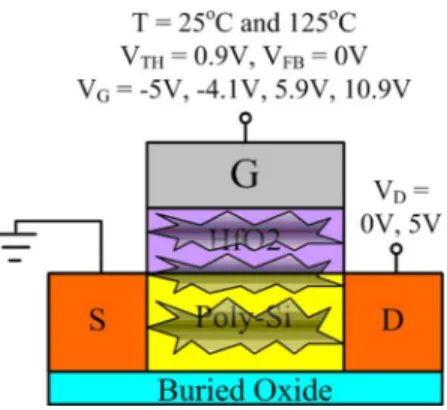
Fig. 1. Cross-section structure of Al/HfO2/poly-Si n-channel LTPS-TFT
with different VGand VD stress biases for 1000 s. The locations of stress
damage are also indicated.
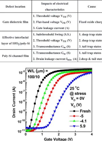
Fig. 2. ID–VGand transconductance Gmcharacteristics of the HfO2
LTPS-TFT with W/L = 100/10 µm.
treatment in the furnace was applied to improve the gate-oxide quality at 400◦C for 30 min. A 75-nm HfO2 with effective oxide thickness of 14.7 nm was measured to indicate a high permittivity of about 20 for HfO2. In addition, a ∼3-nm IL was also observed from the transmission electron microscopy micrograph of HfO2 gate-dielectric LTPS-TFT, which is not shown here. After the patterning of contact holes, aluminum was deposited by thermal-evaporation system and patterned as the probe pads to complete the TFT devices.
The devices with gate length and width of 10 and 100 µm, respectively, were measured. The VTH is defined as the VG at
which the IDreaches 100 nA× W/L and VD= 0.1 V.
Differ-ent gate- and drain-bias stresses are performed at 25◦C and 125◦C, as shown in Fig. 1. The stress of VG=−5, −4.1, 5.9,
and 10.9 V represent VG− VFB=−5 V, VG− VTH=−5, 5, and 10 V, respectively. The flatband voltage VFB is defined as the gate voltage that yields the minimum drain–current from the transfer characteristic [21]. The field-effect mobility µFEis extracted from the maximum transconductance Gm.
III. RESULTS ANDDISCUSSION
Fig. 2 shows the transfer characteristics of the HfO2 LTPS-TFT without any passivation treatment. High-performance HfO2 LTPS-TFT with low threshold voltage VTH ∼ 0.9 V, excellent subthreshold swing S.S. of∼0.147 V/dec, high
field-TABLE I
DEVICE-PARAMETERCOMPARISON OF THEHfO2GATE-DIELECTRIC
TFTS. OTHERGATE-DIELECTRICTFTSARE
ALSOLISTED FORCOMPARISON
effective mobility µEF∼ 74.5 cm2/V· s, and high Ion/Imin current ratio ∼2.19 × 10⁶ is demonstrated to be suitable for the applications of AMLCD and SOP. Some important param-eters are listed in Table I. Compared with the conventional LTPS-TFT with thick SiO2 gate dielectric, as shown in Table I, obviously, the LTPS-TFT with high-κ gate dielectric can lower the threshold voltage VTH, reduce the subthreshold swing S.S., improve the field-effect mobility µFE, and increase the Ion/Imincurrent ratio without any hydrogen-related plasma treatment. The highly improved performance of LTPS-TFT with high-κ gate dielectric can be attributed to the employ-ment of high-κ gate dielectric which can provide much higher gate capacitance density with thicker dielectric thickness and smaller gate leakage current.
In order to study the reliability mechanisms of HfO2 LTPS-TFT, we divided the HfO2 LTPS-TFT into three parts to discuss, as shown in Fig 1. They are the following: gate-dielectric film, effective IL of HfO2/poly-Si, and poly-Si chan-nel film. Because the defects in the HfO2/poly-Si interface are correlated with the defects in the poly-Si grain boundaries of the conduction channel near the HfO2/poly-Si interface, we define the effective IL as the combination of the HfO2/poly-Si inter-face and the grain boundaries of poly-Si near the surinter-face con-duction channel which is about several nanometers below the HfO2/poly-Si interface. Then, the distribution and mechanisms of the defect and trap-state generation will be discussed as follows according to the electrical properties of the HfO2 LTPS-TFT such as threshold voltage VTH, transconductance Gm,
gate leakage current, subthreshold swing S.S., and drain leak-age current Imin.
Based on the proposed degradation mechanisms, the genera-tion of the fixed oxide charge in the gate-dielectric film would affect the threshold voltage VTH and gate leakage current due to the variance in the potential of gate dielectric [22]. The subthreshold swing S.S. would depend on the defects in the effective IL. The deep-trap states existing in the grain bound-aries of the effective IL have been demonstrated to degrade mainly the subthreshold swing S.S. and much less the transcon-ductance Gm [21], [23], [24]. Moreover, the tail-trap states
existing in the grain boundaries of the effective IL would mainly contribute to the degradation of the transconductance Gm
and much less to the subthreshold swing S.S. [21], [23], [24]. In addition, the grain-boundary traps in the channel film would
TABLE II
DEGRADATION OFEXPERIMENTALELECTRICALCHARACTERISTICS AND
CORRESPONDINGPOSSIBLEDEGRADATIONMECHANISMS
Fig. 3. ID–VG characteristics of the HfO2 LTPS-TFT before and after
different gate-bias stresses with fixed VD= 0 V for 1000 s at 25◦C.
also result in the drain leakage current Imin[23], [25]. There-fore, it is obvious that the electrical properties after stress could be used to clarify the generation and distribution of defects and trap states of the LTPS-TFTs. These proposed reliability mechanisms are summarized in Table II.
Fig. 3 shows the ID–VG characteristic of HfO2LTPS-TFT before and after NBS and PBS with VG =−5, −4.1, and 5.9 V
and VD= VS = 0 V for 1000 s at T = 25◦C. The
threshold-voltage shift ∆VTHof PBS is more significant than the ∆VTH of NBS. Both the subthreshold-swing S.S. degradation and the fixed-oxide-charge generation, which is due to carrier injection, could result in the threshold-voltage shift ∆VTH. Fig. 4 shows the subthreshold swing S.S. and the transconductance Gm
of the HfO2LTPS-TFT before and after NBS and PBS, which indicates that more subthreshold-swing S.S. degradation of PBS is observed than that of NBS, resulting in more threshold-voltage shift ∆VTH of PBS than NBS. In addition to the different subthreshold-swing S.S. degradation of NBS and PBS, the flatband voltage shifts ∆VFB of NBS and PBS also show different behaviors. The NBS shows a slight increase of flatband shift ∆VFB, and PBS shows a significant increase of flatband shift ∆VFB. It indicates that more negative fixed charges are produced by PBS than NBS, which means that more electrons are injected into the HfO2from the channel film
Fig. 4. Transconductance Gm and subthreshold swing S.S. of the HfO2
LTPS-TFT before and after different gate-bias stresses with fixed VD= 0 V
for 1000 s at 25◦C.
Fig. 5. Gate leakage current of the HfO2LTPS-TFT before and after different
gate-bias stresses with fixed VD= 0 V for 1000 s at 25◦C.
during PBS than the electron injection from gate during NBS. Electron trapping in HfO2 would raise the electron potential of HfO2 to reduce the tunneling of electrons, resulting in the decrease of gate leakage current. Fig. 5 shows the gate leakage current of the HfO2LTPS-TFT before and after NBS and PBS. A more significant gate-leakage-current reduction after PBS is observed than the one after NBS, which consists in the results of flatband shift ∆VFBthat is due to the electron trapping in HfO2. Therefore, the threshold-voltage shifts ∆VTH of PBS and NBS are mainly attributed to both the subthreshold-swing S.S. degradation and electron trapping in the HfO2, and both the subthreshold-swing S.S. degradation and electron trapping of PBS are more serious than NBS, resulting in more threshold-voltage shift ∆VTH of PBS than NBS. Therefore, we can deduce that both PBS and NBS would produce the deep-trap states in the effective IL because of the subthreshold-swing S.S. degradation. In addition, the PBS degrades the device much more than the NBS does. In addition to the threshold-voltage shift ∆VTHand the subthreshold-swing S.S. degradation, Fig. 4 shows a similar transconductance degradation ∆Gm of PBS
and NBS. Although the transconductance degradation ∆Gmof
PBS and NBS is similar, the mechanisms of transconductance degradation ∆Gm of PBS and NBS are completely different,
Fig. 6. ID–VGand transconductance Gmcharacteristics of the HfO2
LTPS-TFT before and after different gate-bias stresses with fixed VD= 0 V for 1000
s at 125◦C.
Fig. 7. Transconductance Gmand subthreshold-swing S.S. characteristics of
the HfO2 LTPS-TFT before and after different gate-bias stresses with fixed VD= 0 V for 1000 s at 125◦C.
and they will be distinguished in terms of NBTI and PBTI and discussed as follows.
Fig. 6 shows the ID–VG characteristic of HfO2 LTPS-TFT before and after NBTI and PBTI with VG=−5 and 5.9 V
and VD= VS = 0 V for 1000 s at T = 125 ◦C. Similar
subthreshold-swing S.S. degradation and threshold-voltage shift ∆VTHare observed for PBTI and NBTI. However, much more serious transconductance degradation Gm of NBTI is
observed than that of PBTI, as shown in Figs. 6 and 7. In addi-tion, the drain leakage current Iminalso shows the remarkably different behavior that PBTI has a significant drain-leakage-current Imin degradation and NBTI shows a nearly invariant drain leakage current Imin, as shown in Fig. 6, which indicates that the mechanism of NBTI is quite different from that of PBTI. The drain leakage current Imincan be attributed to two sources: One is coming from the gate leakage current, and the other is coming from the junction leakage current of drain side [25]. In this case, the gate leakage current, as shown in Fig. 8, has been shown to be too low to contribute to the drain leakage current Imin of devices. Therefore, we can conclude that the drain-leakage-current Imin degradation is coming from the junction leakage of the drain side, which is close to the surface. In PBTI device, the highest drain-leakage-current Iminincrease
Fig. 8. Gate leakage current of the HfO2LTPS-TFT before and after different
gate-bias stresses with fixed VD= 0 V for 1000 s at 125◦C.
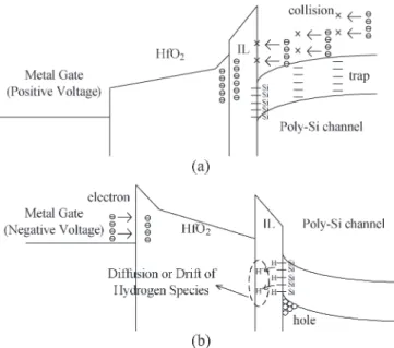
Fig. 9. Energy-band diagram of the HfO2 LTPS-TFT under (a) PBTI and
(b) NBTI stresses.
indicates the most serious grain damage in the channel film, re-sulting in significant increase of the drain leakage current Imin. Therefore, we can deduce that the PBTI would attract electrons from the channel film to inject into the HfO2 gate dielectric. During PBS, electrons would be accelerated by a positive gate voltage, and they move toward the interface of HfO2 /poly-Si, as shown in Fig. 9(a). The accelerated electrons would collide with the weak bond of the grain boundaries and dam-age the poly-Si channel film and the effective IL to generate the trap states to increase the drain leakage current Imin and subthreshold swing S.S. and reduce the transconductance Gm.
In addition to the PBTI, the NBTI would merely damage the effective IL to generate the trap states, increasing the sub-threshold swing S.S. and reducing the transconductance Gm.
Although the PBTI would degrade the grain boundaries of the channel film much more than the NBTI, the NBTI shows the most serious degradation of transconductance Gm. Therefore,
the damage of NBTI would be in the effective IL, which is less dependent on the drain leakage current Imin. Hydrogen
Fig. 10. Transconductance Gmand subthreshold-swing S.S. characteristics
of the HfO2LTPS-TFT before and after different gate-bias stresses with fixed VD= 0 V and VD= 5 V for 1000 s at 25◦C.
diffusion-controlled model, which is the electrochemical reac-tions between the holes and the hydrogen species, has been proposed to be the degradation mechanism of the LTPS-TFTs after NBTI [15], [20]. When an NBS is performed, holes will accumulate at the oxide/Si interface, and they react with the hydrogen species which are weakly bound to Si atoms, as shown in Fig. 9(b). The dissociation of hydrogen will then generate the interface trap states, and this is more important for high-κ gate-dielectric devices due to their high density of trap states. A significant subthreshold-swing S.S. degradation and transconductance Gm reduction indicate that both
deep-trap and tail-deep-trap states are generated after the NBTI stress. The degradation model of LTPS-TFT under the NBTI stress can be described by the following [20]:
[≡Si−H] (interface)+[≡ Si−O−Si ≡] (interfacial oxide)
→[Si•] (interface) + [≡ Si+]
+ [≡ Si−OH] (interfacial oxide) + e−.
The hydrogen atoms are weakly bonded to the Si atoms at the interface of the polysilicon channel film. Under the NBTI stress, hydrogen atoms react with the holes from the inversion layer and dissociate from the Si atoms. The release of hydrogen atoms results in the generation of interface defects to form the deep-trap and tail-trap states and degrade the subthreshold swing S.S. and transconductance Gm, respectively.
Furthermore, a 5-V drain bias is applied during NBS and PBS to investigate the impacts of the drain-bias stress. Fig. 10 shows that more serious transconductance Gm and
subthreshold-swing S.S. degradation of NBS with VD= 5 V
than VD= 0 V are observed. Contrary to the NBS with
drain-bias stress, the PBS with VD= 5 V shows a slight
improve-ment of the transconductance Gmand subthreshold-swing S.S.
degradation compared with PBS with VD= 0 V. In addition,
the NBTI and PBTI with VD= 5 V at T = 125◦C are also
studied, as shown in Fig. 11. The same trend of the transcon-ductance Gm and subthreshold-swing S.S. degradation is also
observed compared with NBS and PBS with drain-bias appli-cation. However, for the PBTI case, the drain leakage current is decreased with VD= 5 V compared with VD= 0 V, as shown
Fig. 11. ID–VG and transconductance Gm characteristics of the HfO2
LTPS-TFT before and after different gate-bias stresses with fixed VD= 5 V
for 1000 s at 125◦C.
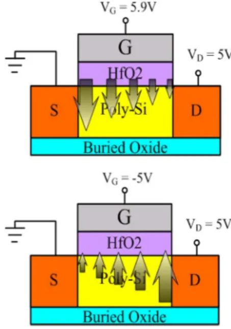
Fig. 12. Cross-section structure of Al/HfO2/poly-Si n-channel LTPS-TFT
with drain-bias stress for 1000 s. The magnitudes of vertical electric field are also indicated.
in Fig. 6. It is because that the application of a drain bias would make the vertical electric field near the drain side becomes lower and improve the drain leakage current Imin slightly. When a larger drain bias was applied during PBTI, the vertical electric field of the channel film would be decreased further. As shown in Fig. 12, applying a drain bias would decrease the vertical field near the drain side and result in less junction damage. Therefore, the large drain bias would make the device to have less drain-leakage-current Imindegradation, and a hump in transfer characteristic of the device is observed, as shown in Fig. 13. For the NBTI case, applying a drain bias would increase the vertical field near the drain side, as shown in Fig. 12, and result in more serious transconductance Gmand
subthreshold-swing S.S. degradation. This appearance of asymmetry damage of the source/drain-junction region is also observed in the previous paper [15], [16]. In addition, the transconductance Gm
of the HfO2 LTPS-TFT would be decreased as the drain-bias increases after VD= 10 V to indicate that the impact-ionization
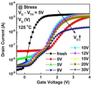
Fig. 13. ID–VGcharacteristics of the HfO2LTPS-TFT before and after
dif-ferent drain-bias stresses with fixed VG− VTH= 5 V for 1000 s at 125◦C.
effect of HCS [16] is appearing, as shown in Fig. 13. Therefore, the stress of vertical electric field is more important than the stress of lateral electrical field for the HfO2 LTPS-TFT before the occurrence of HCS, and the impact ionization of the HfO2 LTPS-TFT dominates the degradation when the large drain-bias stress is applied.
The electron trapping in the gate dielectric and the trap-state generation of channel film and interface regions are observed for both HfO2 and conventional thick SiO2 LTPS-TFTs after PBS stresses [3], [19]. In addition, the significant subthreshold-swing S.S. degradation of HfO2 and SiO2 LTPS-TFTs after NBS stresses is observed [3], [14], [15]. However, the location of trap generation in interface or channel film is difficult to determine after PBS and NBS stresses. The mechanism of NBTI of the LTPS-TFT proposed by Chen et al. would be adopted to explain the behavior of NBS [20]. Therefore, the reliability mechanisms of positive-gate-bias stress and NBS can be systematically analyzed by studying the electrical char-acteristics of LTPS-TFT after NBS, PBS, NBTI, and PBTI stresses.
Comparing the stresses of HfO2 LTPS-TFT with the con-ventional thick SiO2 LTPS-TFT, the effective electric field of stress Eeff in the channel film (Eeff = VG/tdielectric×
εdielectric/εsilicon) is quite different. The tdielectric, εdielectric, and εsilicon are defined as the dielectric thickness, gate-dielectric permittivity, and silicon permittivity, respectively. The stress field of HfO2 LTPS-TFT would be higher than that of the conventional thick SiO2LTPS-TFT. Large gate-bias stress at high temperature can accelerate the degradation to distinguish between positive-gate-bias stress and NBS. The re-markable Imindegradation behavior after PBTI is not observed in previous papers [3], [14], [15], [19] due to higher vertical stress field of HfO2 LTPS-TFT. In addition, the hole trapping in gate dielectric after PBS and PBTI is not found in this paper. It could be due to the characteristic of high-κ gate dielectric in which electron trapping is easier than hole trapping. Moreover, the stress of vertical electric field is the dominant factor for the HCS of HfO2 LTPS-TFT, which is completely different with previous report [19]. It would be due to the characteristic of
high-κ gate dielectric that the ability of charge trapping is more significant than SiO2.
So far, we have analyzed the reliability mechanisms of LTPS-TFT with HfO2gate dielectric. The employment of high-κ gate dielectric gives an effective way to keep the performance of LTPS-TFT at low operation voltage. In addition, many defect passivation methods have been proposed to improve the reli-ability of LTPS-TFT [26], [27]. High-performance and reliable LTPS-TFT with high-κ gate dielectric will be one of the most possible solutions to realize the target of system-on-panel.
IV. CONCLUSION
A comprehensive investigation of the reliability mechanisms of high-performance LTPS-TFT with HfO2 gate dielectric is reported for the first time. Various stress conditions, including PBS, PBTI, NBS, NBTI, and HCS, are performed to differenti-ate the degradation mechanisms. For PBS and PBTI, it is found that serious subthreshold-swing S.S. degradation is due to the deep-trap states of the effective IL; the transconductance Gm
decrease with the drain-leakage-current Iminincrease is due to the tail-trap states of poly-Si grain boundaries, and the gate-leakage-current reduction is due to electron trapping of the HfO2 gate dielectric. For NBS and NBTI, significant sub-threshold swing S.S. and transconductance Gm degradation
without the drain-leakage-current Imin increase are observed to show that the effective IL is the main damage region and that both deep- and tail-trap states are generated after NBS and NBTI. Remarkable drain-leakage-current Iminincrease of PBTI and almost invariant drain-leakage-current Imin degra-dation of NBTI show that the PBTI and NBTI are attributing to different mechanisms. The carrier collision and injection model is employed to explain the mechanisms of PBS and PBTI, and the hydrogen-diffusion model is employed to explain the mechanisms of NBS and NBTI. In addition, the drain-bias application during stress is also studied, and the results show that the impact ionization will dominate the degradation mechanism if a large drain-bias stress is used.
ACKNOWLEDGMENT
The authors would like to thank the processes support from the National Nano Device Labs and the Nano Facility Center of the National Chiao Tung University.
REFERENCES
[1] G. K. Guist and T. W. Sigmon, “High-performance thin-film transistors fabricated using excimer laser processing and grain engineering,” IEEE
Trans. Electron Devices, vol. 45, no. 4, pp. 925–932, Apr. 1998.
[2] Y. W. Choi, J. N. Lee, T. W. Jang, and B. T. Ahn, “Thin-film transistors fabricated with poly-silicon films crystallized at low temperature by mi-crowave annealing,” IEEE Electron Device Lett., vol. 20, no. 1, pp. 2–4, Jan. 1999.
[3] C. W. Lin, M. Z. Yang, C. C. Yeh, L. J. Cheng, T. Y. Huan, H. C. Cheng, H. C. Lin, T. S. Chao, and C. Y. Chang, “Effects of plasma treat-ments, substrate types, and crystallization methods on performance and reliability of low temperature polysilicon TFTs,” in IEDM Tech. Dig., 1999, pp. 305–308.
[4] K. M. Chang, W. C. Yang, and C. P. Tsai, “Electrical characteristics of low temperature polysilicon TFT with a novel TEOS/oxynitride stack gate dielectric,” IEEE Electron Device Lett., vol. 24, no. 8, pp. 512–514, Aug. 2003.
[5] J.-H. Jeon, M.-C. Lee, K.-C. Park, S.-H. Jung, and M.-K. Han, “A new poly-Si TFT with selectively doped channel fabricated by novel excimer laser annealing,” in IEDM Tech. Dig., 2000, pp. 213–216.
[6] J. Y. W. Seto, “The electrical properties of polycrystalline silicon films,”
J. Appl. Phys., vol. 46, no. 12, pp. 5247–5254, Dec. 1975.
[7] G. D. Wilk, R. M. Wallace, and J. M. Anthony, “High-κ gate dielectrics: Current status and material properties considerations,” J. Appl. Phys., vol. 89, no. 10, pp. 5243–5275, May 2001.
[8] B. F. Hung, K. C. Chiang, C. C. Huang, A. Chin, and S. P. McAlister, “High-performance poly-silicon TFTs incorporating LaAlO3as the gate
dielectric,” IEEE Electron Device Lett., vol. 26, no. 6, pp. 384–386, Jun. 2005.
[9] Z. Jin, H. S. Kwok, and M. Wong, “High-performance polycrystalline SiGe thin-film transistors using Al2O3 gate insulators,” IEEE Electron Device Lett., vol. 19, no. 12, pp. 502–504, Dec. 1998.
[10] C.-P. Lin, B.-Y. Tsui, M.-J. Yang, R.-H. Huang, and C. H. Chien, “High-performance poly-silicon TFTs using HfO2gate dielectric,” IEEE Elec-tron Device Lett., vol. 27, no. 5, pp. 360–363, May 2006.
[11] C. Hoobs, H. Tseng, K. Reid, B. Taylor, L. Hebert, R. Garcia, R. Hegde, J. Grant, D. Gilmer, A. Franke, V. Dhandapani, M. Azrak, L. Prabhu, R. Rai, S. Bagchi, J. Conner, S. Backer, F. Dumbuya, B. Nguyen, and P. Tobin, “80 nm poly-Si gate CMOS with HfO2gate dielectric,” in IEDM Tech. Dig., 2001, pp. 651–654.
[12] Y. Kim, C. Lim, C. D. Young, K. Mathews, J. Barnett, B. Foran, A. Agrawal, G. A. Brown, G. Bersuker, P. Zeitzoff, M. Gardner, R. W. Murto, L. Larson, C. Metzner, S. Kher, and H. R. Huff, “Con-ventional poly-Si gate MOS-transistors with a novel, ultra-thin Hf-oxide layer,” in VLSI Symp. Tech. Dig., 2003, pp. 167–168.
[13] C.-Y. Chen, J.-W. Lee, P.-H. Lee, W.-C. Cheng, H.-Y. Lin, K.-L. Yeh, M.-W. Ma, S.-D. Wang, and T.-F. Lei, “A reliability model for low-temperature polycrystalline silicon thin-film transistors,” IEEE Electron
Device Lett., vol. 28, no. 5, pp. 392–394, May 2007.
[14] N. D. Young and J. R. Ayres, “Negative gate bias instability in poly-crystalline silicon TFTs,” IEEE Trans. Electron Devices, vol. 42, no. 9, pp. 1623–1627, Sep. 1995.
[15] C.-Y. Chen, J.-W. Lee, M.-W. Ma, W.-C. Cheng, H.-Y. Lin, K.-L. Yeh, S.-D. Wang, and T.-F. Lei, “Bias temperature instabilities for low-temperature polycrystalline silicon complementary thin-film transis-tors,” J. Electrochem. Soc., vol. 154, no. 8, pp. H704–H707, 2007. [16] A. T. Hatzopoulos, D. H. Tassis, N. A. Hastas, C. A. Dimitriadis, and
G. Kamarinos, “An analytical hot-carrier induced degradation model in polysilicon TFTs,” IEEE Trans. Electron Devices, vol. 52, no. 10, pp. 2182–2187, Oct. 2005.
[17] F. V. Farmakis, J. Brini, G. Kamarinos, and C. A. Dimitriadis, “Anomalous turn-on voltage degradation during hot-carrier stress in polycrystalline silicon thin-film transistors,” IEEE Electron Device Lett., vol. 22, no. 2, pp. 74–76, Feb. 2001.
[18] A. T. Hatzopoulos, D. H. Tassis, N. A. Hastas, C. A. Dimitriadis, and G. Kamarinos, “On-state drain current modeling of large-grain poly-crystalline silicon thin-film transistors,” IEEE Trans. Electron Devices, vol. 52, no. 8, pp. 1727–1733, Aug. 2005.
[19] I. W. Wu, W. B. Jackson, T. Y. Huang, A. G. Lewis, and A. Chiang, “Mechanism of device degradation in n-channel and p-channel polysilicon TFTs by electrical stressing,” IEEE Electron Device Lett., vol. 11, no. 3, pp. 167–169, Mar. 1990.
[20] C.-Y. Chen, J.-W. Lee, S.-D. Wang, M.-S. Shieh, P.-H. Lee, W.-C. Cheng, H.-Y. Lin, K.-L. Yeh, and T.-F. Lei, “Negative bias temperature instabil-ity in low-temperature polycrystalline silicon thin-film transistors,” IEEE
Trans. Electron Devices, vol. 53, no. 12, pp. 2993–3000, Dec. 2006.
[21] J. Levinson, F. R. Shepherd, P. J. Scanlon, W. D. Westwood, G. Este, and M. Rider, “Conductivity behavior in polycrystalline semiconductor thin film transistors,” J. Appl. Phys., vol. 53, no. 2, pp. 1193–1202, Feb. 1982. [22] K. Onishi, R. Choi, C. S. Kang, H.-J. Cho, Y. H. Kim, R. E. Nieh, J. Han, S. A. Krishnan, M. S. Akbar, and J. C. Lee, “Bias-temperature instabilities of polysilicon gate HfO2 MOSFETs,” IEEE Trans. Electron Devices,
vol. 50, no. 6, pp. 1517–1524, Jun. 2003.
[23] I.-W. Wu, T.-Y. Huang, W. B. Jackson, A. G. Lewis, and A. Chiang, “Passivation kinetics of two types of defects in polysilicon TFT by plasma hydrogenation,” IEEE Electron Device Lett., vol. 12, no. 4, pp. 181–183, Apr. 1991.
[24] I.-W. Wu, A. G. Lewis, T.-Y. Huang, and A. Chiang, “Effects of trap-state density reduction by plasma hydrogenation in low-temperature polysil-icon TFT,” IEEE Electron Device Lett., vol. 10, no. 3, pp. 123–125, Mar. 1989.
[25] K. R. Plasupo and M. K. Hatalis, “Leakage current mechanisms in sub-micron polysilicon thin-film transistors,” IEEE Trans. Electron Devices, vol. 43, no. 8, pp. 1218–1223, Aug. 1996.
[26] S.-D. Wang, W.-H. Lo, and T.-F. Lei, “CF4plasma treatment for
fabricat-ing high-performance and reliable solid-phase-crystallized poly-Si TFTs,”
J. Electrochem. Soc., vol. 152, no. 9, pp. 703–706, 2005.
[27] C.-H. Tu, T.-C. Chang, P.-T. Liu, C.-H. Chen, C.-Y. Yang, Y.-C. Wu, H.-C. Liu, L.-T. Chang, C.-C. Tsai, S. M. Sze, and C.-Y. Chang, “Electri-cal enhancement of solid phase crystallized poly-Si thin-film transistors with fluorine ion implantation,” J. Electrochem. Soc., vol. 153, no. 9, pp. 815–818, 2006.
Ming-Wen Ma was born in Taipei, Taiwan, R.O.C.,
in 1980. He received the B.S. degree in electro-physics and the M.S. degree in electronics engi-neering from the National Chiao Tung University, Hsinchu, Taiwan, in 2002 and 2004, respectively, where he is currently working toward the Ph.D. degree in the Institute of Electronics.
His research interests are the fabrication and characterization of low-temperature polycrystalline thin-film transistor, silicon-on-insulator device, metal-gate/high-κ technology, and RF metal insulator–metal capacitor.
Chih-Yang Chen was born in Changhua, Taiwan,
R.O.C., on December 19, 1980. He received the Ph.D. degree in electronics engineering from the National Chiao Tung University, Hsinchu, Taiwan, in 2007.
He is currently with the Institute of Electronics, National Chiao Tung University. His research inter-ests are the fabrication process and reliability of low-temperature poly-Si thin-film transistors.
Woei-Cherng Wu was born in Taipei, Taiwan,
R.O.C., on December 26, 1978. He received the B.S. and M.S. degrees in electronics engineering from Chang Gung University, Taoyuan, Taiwan, in 2002 and 2004, respectively. He is currently work-ing toward the Ph.D. degree in the Institute and Department of Electrophysics, National Chiao Tung University, Hsinchu, Taiwan.
His research interest focuses on the studies of semiconductor device physics including high-κ gate dielectrics and nonvolatile Flash memories.
Chun-Jung Su (S’06) was born in Tainan, Taiwan,
R.O.C., in 1979. He received the B.S. degree in mate-rial science and engineering from the National Chiao Tung University, Hsinchu, Taiwan, in 2002, where he is currently working toward the Ph.D. degree in the Institute of Electronics.
His research interests are the fabrication and char-acterization of Si nanowire FETs and biosensing devices.
Kuo-Hsing Kao was born in Taipei, Taiwan, R.O.C.,
in 1982. He received the B.S. degree in physics from the National Chung Hsing University, Taichung, Taiwan, in 2005. He is currently working toward the M.S. degree in the Institute and Department of Electrophysics, National Chiao Tung University, Hsinchu, Taiwan.
His research interests are high-κ gate dielectrics and device physics.
Tien-Sheng Chao (S’88–M’92–SM’01) was born
in Penghu, Taiwan, R.O.C., in 1963. He received the Ph.D. degree in electronics engineering from the National Chiao Tung University, Hsinchu, Taiwan, in 1992.
In 1992, he was an Associate Researcher with the National Nano Device Laboratories and be-came a Researcher in 1996. He was engaged in developing the thin dielectrics preparations, clean-ing processes, and CMOS device fabrication. Since 2001, he has been with the Institute and Department of Electrophysics, National Chiao Tung University. He has published over 140 papers in this field.
Tan-Fu Lei (M’98) was born in Keelung, Taiwan,
R.O.C., on September 17, 1944. He received the B.S. degree in electrical engineering from the National Cheng Kung University, Tainan, Taiwan, in 1967 and the M.S. and Ph.D. degrees in electronics en-gineering from the National Chiao Tung University, Hsinchu, Taiwan, in 1970 and 1979, respectively.
From 1970 to 1972, he was with the Fine Products Microelectronics Corporation, Taipei, Taiwan, as an Engineer, working on the fabrication of small-signal transistors. From 1980 to 1982, he was the Plant Manager with SINTEK Photronic Corporation, Hsinchu. Since 1983, he has been an Associate Professor with the Department of Electronics Engineering and the Institute of Electronics, National Chiao Tung University, where he is the Director of the Semiconductor Research Center from 1984 to 1986 and the Deputy Director of the National Nano Device Laboratories from 1991 to 1998. He is currently a Professor with the Department of Electronics Engineering and the Institute of Electronics, National Chiao Tung University. His research inter-ests are semiconductor devices and very large scale integration technologies.