double-quantum-barrier [TaN
− Ir3
Si]
− [HfAlO − LaAlO3
]
−
Hf
0.3N
0.2O
0.5− [HfAlO − SiO2
]-Si charge-trapping memory
devices. These devices display good characteristics in terms
of their
±9-V program/erase (P/E) voltage, 100-µs P/E speed,
initial 3.2-V memory window, and ten-year extrapolated data
retention window of 2.4 V at 150
◦C. The retention decay rate
is significantly better than single-barrier MONOS devices, as
is the cycled retention data, due to the reduced interface trap
generation.
Index Terms—Erase, high-κ, nonvolatile memory, program.
I. I
NTRODUCTIONM
ETAL-OXIDE-NitriOxiSilicon (MONOS)
de-vices [1]–[13] are attractive candidates for highly scaled
sub-50-nm nonvolatile memories (NVMs). This is due to
their discrete charge-trapping property, which can avoid stored
charge leakage via a single oxide defect, when compared with
conventional conductive poly-Si floating-gate memory devices.
However, good data retention at high temperatures is difficult in
MONOS memory—this is due to the shallower trap energy in
Si
3N
4[14] when compared with poly-Si floating-gate memory,
which displays a 3.2-eV trap energy. To address this issue, we
previously used deep trap-energy Al(Ga)N and HfON to replace
the Si
3N
4in MONOS devices [10]–[12], leading to improved
retention when compared with Si
3N
4[13]. Unfortunately, the
85
◦C retention showed a charge decay (at 42%–46% of the
ini-tial memory window) that was relatively high and unacceptable.
The high temperature retention can be improved via
bandgap-engineered SONOS (BE-SONOS) [9], but the erase speed is
Manuscript received February 15, 2008; revised April 15, 2008. This work was supported in part by the National Science Council of Taiwan, R.O.C., under Grant 95-2221-E-009-275. The review of this paper was arranged by Editor M. J. Kumar.
S. H. Lin and F. S. Yeh are with the Institute of Electronics Engineering, Department of Electrical Engineering, National Tsing-Hua University, Hsinchu 300, Taiwan, R.O.C.
H. J. Yang and W. B. Chen are with the Department of Electronics Engineer-ing, National Chiao-Tung University, Hsinchu 300, Taiwan, R.O.C.
S. P. McAlister is with the Institute for Microstructural Sciences, National Research Council of Canada, Ottawa, ON K1A 0R6, Canada.
A. Chin is with the Department of Electronics Engineering, National Chiao-Tung University, Hsinchu 300, Taiwan, R.O.C., and also with the Nano-Electronics Consortium of Taiwan, Hsinchu 300, Taiwan, R.O.C. (e-mail: [email protected]).
Color versions of one or more of the figures in this paper are available online at http://ieeexplore.ieee.org.
Digital Object Identifier 10.1109/TED.2008.924435
(18–20 V), contrary to the requirements of the ITRS scaling
roadmap.
In this paper, we report a new double-quantum-barrier
charge-trapping NVM device with good high temperature
re-tention, low P/E voltages, and high speed. For instance, for a
9-V P/E voltage applied between the gate and Si channel at
100 µs, the extrapolated ten-year retention window was 2.4 V at
150
◦C, where the initial value was 3.2 V. The observed
reten-tion P/E decay at this temperature was only 82/26 mV/decade
(or 25% of the initial memory window), which is better than
that of Ga(Al)N [10], [11] and HfON [12] MONOS devices.
This is due to the double quantum barriers comprising the lower
[HfAlO
− SiO
2] and the upper [LaAlO
3− HfAlO], which
con-fine the carriers trapped in the deep energy Hf
0.3O
0.5N
0.2quan-tum well. The high electric field across the [HfAlO
− SiO
2]
tunnel oxide leads to the 100-µs P/E speed. For the
double-barrier devices, we have found good 10
5cycling and cycled
retention characteristics, which arise from the rapid 100-µs
P/E—this produces less stress to the tunnel oxide and, thus,
less interfacial trap generation than in the single-barrier devices.
By using
±4.5- and ∓4.5-V P/E voltages applied between the
gate and channel, these devices are promising candidates for
embedded SoC applications using a 5-V voltage source [12].
II. E
XPERIMENTALD
ETAILSThe [TaN
− Ir
3Si]
− [HfAlO − LaAlO
3]
− Hf
0.3N
0.2O
0.5−
[HfAlO
− SiO
2]
− Si NVM device design involved choices of
the oxide barrier height and its thickness. First, a 2.5-nm-thick
thermal SiO
2layer was grown on a standard p-Si substrate
and a 2-nm layer of HfAlO was deposited by PVD to form
the double tunneling layers. Then, a 10-nm Hf
0.3N
0.2O
0.5layer was deposited by reactive sputtering, under mixed O
2and N
2conditions [12], [15]. (The composition of N and O
in the Hf
1−x−yN
xO
ywas measured by X-ray photoelectron
spectroscopy.) An 8-nm LaAlO
3layer and then a 7-nm HfAlO
were deposited to form the double blocking layers. Finally, a
15-nm Ir
3Si and a 150-nm TaN layer was added by PVD. The
high work function Ir
3Si gate was used to make metal-gate/
high-κ p-MOSFETs [16]. After standard processing, the
MONOS devices were fabricated by using self-aligned As
+ion
implantation and given a 950
◦C 30-s rapid thermal anneal
acti-vation to form the source–drain regions. For comparison, we
al-so fabricated a TaN
− HfLaON − Hf
0.3N
0.2O
0.5− SiO
2− Si
Fig. 1. Band diagrams of (a) [Metal-gate]-[High-κ barrier]-[Trapping Layer]-SiO2-Si MONOS nonvolatile memory device and (b) [Metal-gate]-[High-κ
top barrier 1-High-κ top barrier 2]-[Trapping Layer]-[High-κ bottom barrier 2-SiO2]-Si double-quantum-barrier charge-trapping NVM. The conventional
SiN trapping layer is shown in dotted lines.
single-barrier MONOS device. This device had a 2.9-nm-thick
thermal SiO
2, a 9-nm Hf
0.3N
0.2O
0.5trapping layer, and a
15-nm HfLaON blocking oxy-nitride layer. Other procedures
were the same as for the double-barrier device. The equivalent
oxide thickness (EOT) of the [HfAlO
− SiO
2] tunnel oxide in
the double-quantum-barrier device is 3.0 nm, which is close
to the 2.9-nm SiO
2tunnel oxide used in the single-barrier
MONOS device. The EOT of the [HfAlO
− SiO
2] blocking
oxide in the double-barrier device is 3.0 nm—the same as the
single-barrier HfLaON MONOS device. Hence, the EOTs of
both the top blocking oxide and bottom tunnel oxide are almost
the same for both the double- and single-barrier charge-trapping
memory. The memory devices were characterized by different
P/E tests, retention experiments, and cycling endurance at
25
◦C, 85
◦C, and 125
◦C.
III. R
ESULTS ANDD
ISCUSSIONA. Band Diagram and P/E Characteristics
In Fig. 1(a) and (b), we compare the schematic band
dia-grams of the single- and double-quantum-barrier devices,
re-spectively. The conventional SiN trapping layer has a small
conduction band discontinuity (∆E
C) with respect to the
bar-rier oxide of only 1.1 eV [14], where the stored charges in
shallow trap energy levels can leak out at elevated temperatures.
The other ∆E
Cand valence band discontinuity (∆E
V) values
Fig. 2. C–V hysteresis for double-quantum-barrier device showing a large Vthshift.
are from published literature [16]–[18]. Thus, the SiN MONOS
devices are expected to have poor retention properties. The
retention in charge-trapping memory can be improved by
in-creasing ∆E
Cwith respect to the barrier oxide, for instance, by
using Al(Ga)N and HfON when compared with SiN [10]–[12].
The use of Hf
0.3N
0.2O
0.5gives a deeper ∆E
Cof 2.5 eV [16]
compared with SiN [14], Al(Ga)N [10], [11], and our
previ-ously reported HfNO with N–10% [12]. However, the trapped
carriers can still escape via sequential Schottky emission and
tunneling at higher temperatures in the 85
◦C–150
◦C range. For
NVM devices, good 85
◦C–150
◦C retention is required because
of the increasing chip temperatures arising from the higher
power dissipation and larger density of future ICs. As a result,
the double-quantum-barrier structure is useful to improve the
trapped carrier confinement within the Hf
0.3N
0.2O
0.5quantum
well, with its deep trapping energy.
Fig. 2 shows the C–V
hysteresis characteristics of
the double-quantum-barrier charge-trapping device with its
Hf
0.3N
0.2O
0.5trapping layer. The hysteresis window increases
with increasing voltage, indicating good charge storage. A large
hysteresis window of 7.3 V was measured under swept voltages
of
±10 V in this device, which suggests a high trap density
and/or deep trap energy in the Hf
0.3N
0.2O
0.5[10]–[12].
In Fig. 3(a) and (b), the P/E characteristics are displayed for
various gate voltages, for single- and double-quantum-barrier
devices, respectively. The devices had the same Hf
0.3N
0.2O
0.5trapping layer and almost the same EOT for the barrier oxides.
The threshold voltage change (∆V
th) increases with increasing
P/E voltage and time due to the increased number of trapped
charges. For the single-quantum-barrier MONOS device, a
memory window of 2.8 V was obtained at
±9 V and at 100-µs
P/E. For comparison, the double-quantum-barrier
charge-trapping device showed a larger ∆V
thmemory window of 3.2 V
for the same testing conditions. It is noticed that the ∆V
thfor both program and erase are improved compared with that
of the single-barrier device. The combined [HfAlO
− SiO
2]
tunnel oxide, with its EOT close to that for the single-barrier
MONOS device, gives a lower energy barrier for electrons to
tunnel through and leads to a larger memory window. The better
erase characteristics are due to the higher work function of
Ir
3Si gate electrode than that of TaN in single-barrier device.
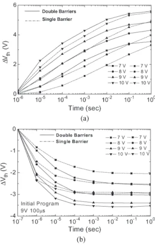
Fig. 3. Comparison of (a) program and (b) erase characteristics between single- and double-quantum-barrier devices under different voltages and times. For the erase, both devices were initially programmed at 9 V for 100 µs.
In both cases, the low P/E voltage arises from the small voltage
drop and electric field (E) in the high-κ barriers and the high-κ
Hf
0.3N
0.2O
0.5(κ = 22) trapping well. This also gives a high
E in the tunnel oxide to produce the high P/E speed using
tunneling mechanism. Because an inverter circuit can be used
to generate the opposite polarities of
±4.5 and ∓4.5 V applied
between the gate and channel [12], this low P/E voltage is
important for embedded SoC applications using a 5-V voltage
source.
B. Retention and Endurance
Good data retention is a challenge for MONOS
charge-trapping memory. Fig. 4(a) shows the retention characteristics
of the single-quantum-barrier MONOS device. The initial ∆V
thwas 2.8 V under 100 µs and
±9-V P/E, and the extrapolated
ten-year memory windows were 2.1, 1.8, and 1.5 V at 25
◦C,
85
◦C, and 125
◦C, respectively. The decay rates at 85
◦C and
125
◦C were 92 and 110 mV/dec for the high state or 36 and
55 mV/dec for the low state. For comparison, in Fig. 4(b), we
show the retention data of a double-quantum-barrier
charge-trapping device at 25
◦C, 85
◦C, and 150
◦C. The initial ∆V
thwas 3.2 V under 100 µs and
±9-V P/E, and the extrapolated
ten-year memory windows were 3.0, 2.7, and 2.4 V under 25
◦C,
85
◦C, and 150
◦C, respectively. The retention P/E decay rates
at 85
◦C and 150
◦C were only 62 and 82 mV/dec for the
Fig. 4. Device retention characteristics of (a) single- and (b) double-quantum-barrier charge-trapping devices at different temperatures.
high state and 15 and 26 mV/dec for the low state (16%
and 25% of initial memory window). This improvement in
the high temperature data retentions, compared with a
single-barrier MONOS device, indicates the advantage of using double
quantum barriers to confine the trapped charges. Because the
EOT is close for both single- and double-barrier devices, using
physically thicker high-κ tunnel layers can improve retention
in double-barrier devices. Using double blocking layer may
also improve the retention due to the slightly higher ∆E
Cand
misaligned trap energies similar to the ONO blocking oxide
case. The read disturbance may be a concern in this low voltage
operated device to cause charge loss. A similar low voltage P/E
at 10 V/
−9 V was also reported, where the stored charges were
not largely lost as evident from the small V
thchange even after
1000 s of gate stresses [19].
Endurance is another important factor for NVM. In Fig. 5(a),
we compare endurance data for single- and double-barrier
charge-trapping devices. Windows of 2.4 and 2.9 V (after
10
5cycles) were obtained for the single- and double-barrier
devices, respectively. This arises from the rapid 100-µs P/E
at 9 V, which causes reduced electric field stress to the tunnel
oxide. The degradation after 10
5cycles is better for the
double-barrier device than that for the single-double-barrier device, with ∆V
thdegradations of 0.3 and 0.4 V or 9% and 14%, respectively.
The effect of long-term cycling on the retention appears in
Fig. 5(b), where the 10
3-cycle ten-year retention windows of
Fig. 5. Comparison of (a) endurance and (b) retention characteristics after 103
P/E cycling of single- and double-quantum-barrier devices.
1.7 and 2.5 V are shown for the single- and
double-quantum-barrier devices, which were initially 2.8 and 3.2 V, respectively.
To understand such improvement, we also measured the
Id
–V
gcharacteristics of the devices before and after cycling.
As shown in Fig. 6, the single-barrier MONOS device shows
an increase of subthreshold swing (SS) with increasing cycling
stress, which suggests the generation of SiO
2/Si interface
traps. In contrast, the double-barrier device shows the same SS
after cycling. Besides the SS change, a shift of I
d–V
gcurves
was also found for both devices after cycling. The
cycling-induced linear I
d–V
gshift or ∆V
thin Fig. 5(a) is also slightly
larger for single-barrier devices than the double-barrier ones,
indicating a slightly larger amount of oxide charge generation.
The generation of SiO
2/Si interface traps in the single-barrier
MONOS device from degraded SS also explains the relative
poor retention after cycling, as shown in Fig. 5(b), because the
trapped carriers may tunnel out via these low energy interface
traps within the Si bandgap.
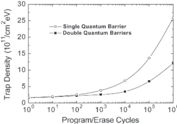
We examined the interface trap generation by charge
pump-ing methods [20]. Fig. 7 shows the interface trap density
(D
it) of single- and double-quantum-barrier devices after P/E
cycling. The initial D
itis nearly the same for both devices.
However, under extensive P/E cycling, more interface traps are
created for the single- than for the double-barrier device. This
improved D
itgeneration in the double-barrier device leads to
better retention after cycling, which is a key factor for achieving
good device integrity for NVM.
Fig. 6. Id–Vg characteristics of (a) single- and (b) double-quantum-barrier
devices after cycling.
Fig. 7. Comparison of the interface trap densities (Dit) for single- and
double-barrier devices after P/E cycling.
IV. C
ONCLUSIONAt 150
◦C under a fast 100-µs and low
±9-V P/E voltage, we
show that a double-quantum-barrier [TaN
− Ir
3Si]
− HfAlO −
LaAlO
3−Hf
0.3O
0.5N
0.2−HfAlO−SiO
2−Si charge-trapping
device has good NVM integrity in terms of a 3.2-V
ini-tial ∆V
thand 2.4-V ten-year extrapolated retention.
Com-pared with its single-quantum-barrier MONOS counterpart, the
double-quantum-barrier device showed significantly better high
temperature retention and cycled retention data, due to better
[4] C. H. Lee, K. I. Choi, M. K. Cho, Y. H. Song, K. C. Park, and K. Kim, “A novel SONOS structure of SiO2/SiN/Al2O3 with TaN
metal gate for multi-giga bit flash memories,” in IEDM Tech. Dig., 2003, pp. 613–616.
[5] C. W. Oh, S. D. Suk, Y. K. Lee, S. K. Sung, J.-D. Choe, S.-Y. Lee, D. U. Choi, K. H. Yeo, M. S. Kim, S.-M. Kim, M. Li, S. H. Kim, E.-J. Yoon, D.-W. Kim, D. Park, K. Kim, and B.-I. Ryu, “Damascence gate FinFET SONOS memory implemented on bulk silicon wafer,” in IEDM
Tech. Dig., 2004, pp. 893–896.
[6] M. Specht, R. Kommling, L. Dreeskornfeld, W. Weber, F. Hofmann, D. Alvarez, J. Kretz, R. J. Luyken, W. Rosner, H. Reisinger, E. Landgraf, T. Schulz, J. Hartwich, M. Stadele, V. Klandievski, E. Hartmann, and L. Risch, “Sub-40 nm tri-gate charge trapping nonvolatile memory cells for high-density applications,” in VLSI Symp. Tech. Dig., 2004, pp. 244–245.
[7] X. Wang, J. Liu, W. Bai, and D.-L. Kwong, “A novel MONOS-type nonvolatile memory using high-κ dielectrics for improved data retention and programming speed,” IEEE Trans. Electron Devices, vol. 51, no. 4, pp. 597–602, Apr. 2004.
[8] Y. N. Tan, W. K. Chim, W. K. Choi, M. S. Joo, T. H. Ng, and B. J. Cho, “High-κ HfAlO charge trapping layer in SONOS-type non-volatile memory device for high speed operation,” in IEDM Tech. Dig., 2004, pp. 889–892.
[9] H. T. Lue, S. Y. Wang, E. K. Lai, Y. H. Shih, S. C. Lai, L. W. Yang, K. C. Chen, J. Ku, K. Y. Hsieh, R. Liu, and C. Y. Lu, “A bandgap engineered SONOS with excellent performance and reliability,” in IEDM
Tech. Dig., 2005, pp. 555–558.
[10] C. H. Lai, A. Chin, K. C. Chiang, W. J. Yoo, C. F. Cheng, S. P. McAlister, C. C. Chi, and P. Wu, “Novel SiO2/AlN/HfAlO/IrO2
memory with fast erase, large ∆Vthand good retention,” in VLSI Symp. Tech. Dig., 2005, pp. 210–211.
[11] A. Chin, C. C. Laio, K. C. Chiang, D. S. Yu, W. J. Yoo, G. S. Samudra, S. P. McAlister, and C. C. Chi, “Low voltage high speed SiO2/AlGaN/
AlLaO3/TaN memory with good retention,” in IEDM Tech. Dig., 2005,
pp. 165–168.
[12] C. H. Lai, A. Chin, H. L. Kao, K. M. Chen, M. Hong, J. Kwo, and C. C. Chi, “Very low voltage SiO2/HfON/HfAlO/TaN memory with fast
speed and good retention,” in VLSI Symp. Tech. Dig., 2006, pp. 54–55. [13] K. H. Joo, C. R. Moon, S. N. Lee, X. Wang, J. K. Yang, I. S. Yeo,
D. Lee, O. Nam, U. I. Chung, J. T. Moon, and B. I. Ryu, “Novel charge trap devices with NCBO trap layers for NVM or image sensor,” in IEDM
Tech. Dig., 2006, pp. 979–982.
[14] S. H. Gu, T. Wang, W. P. Lu, Y. H. Ku, and C. Y. Lu, “Extraction of nitride trap density from stress induced leakage current in silicon-oxide-nitride-oxide-silicon flash memory,” Appl. Phys. Lett., vol. 89, no. 16, p. 163 514, Oct. 2006.
[15] H. J. Yang, A. Chin, W. J. Chen, C. F. Chen, W. L. Huang, I. J. Hsieh, and S. P. McAlister, “A program-erasable high-κ Hf0.3N0.2O0.5MIS
ca-pacitor with good retention,” IEEE Electron Device Lett., vol. 28, no. 10, pp. 913–915, Oct. 2007.
[16] C. H. Wu, B. F. Hung, A. Chin, S. J. Wang, X. P. Wang, M.-F. Li, C. Zhu, Y. Jin, H. J. Tao, S. C. Chen, and M. S. Liang, “High temperature stable [Ir3Si-TaN]/HfLaON CMOS with large work-function difference,”
in IEDM Tech. Dig., 2006, pp. 617–620.
[17] J. Robertson, “Band offsets of wide-band-gap oxides and implications for future electron devices,” J. Vac. Sci. Technol. B, Microelectron. Process.
Phenom., vol. 18, no. 3, pp. 1785–1791, May 2000.
[18] H. Y. Yu, M. F. Li, B. J. Cho, C. C. Yeo, and M. S. Joo, “Energy gap and band alignment for (HfO2)x(Al2O3)1−xon (100) Si,” Appl. Phys. Lett., vol. 81, no. 2, pp. 376–378, Jul. 2002.
in 2004 and the M.S. degree from the Department of Electrical Engineering, National Sun Yat-Sen Uni-versity, Kaohsiung, Taiwan, in 2006. He is currently working toward the Ph.D. degree in the Institute of Electronics Engineering, Department of Elec-trical Engineering, National Tsing-Hua University, Hsinchu, Taiwan.
His current research interests include high-κ/ metal gate CMOS devices, low temperature shallow junctions, MIM DRAM capacitors, and nonvolatile memory device applications.
H. J. Yang received the B.S. degree from Chung
Hsing University, Taichung, Taiwan, R.O.C., in 2002 and the M.S. and Ph.D. degrees from the Depart-ment of Electronics Engineering, National Chiao-Tung University, Hsinchu, Taiwan, in 2004 and 2008, respectively.
He is currently with the Department of Electron-ics Engineering, National Chiao-Tung University. His current research interests include high-κ/ metal gate materials for nonvolatile memory device applications.
W. B. Chen received the B.S. degree in industrial
technology education from the National Kaohsiung Normal University, Kaohsiung Taiwan, R.O.C., in 2006. He is currently working toward the Ph.D. degree in electronics engineering at the National Chiao-Tung University, Hsinchu, Taiwan.
His current research interests include nonvolatile memory and Ge MOSFETs.
F. S. Yeh received the Ph.D. degree in physics from
Wayne State University, Detroit, MI.
Since 1980, she has been with the Department of Electrical Engineering, Tsing-Hua University, Hsinchu, Taiwan, R.O.C., and has been working on spin glass, amorphous Si devices, Si doping in GaAs, GaAs MESFET, and ultrathin oxynitride. Currently, she is a Professor and is engaged in the development of silicide technology, barrier metal, and multilevel metallization.
Sean P. McAlister (SM’02) was born in Durban,
South Africa. He received the M.Sc. degree in physics from the University of Natal, Natal, South Africa, in 1968 and the Ph.D. degree in physics from Cambridge University, Cambridge, U.K., in 1971.
After four years with Simon Fraser University, Vancouver, BC, Canada, he joined the National Re-search Council (NRC) of Canada, Ottawa, ON, in 1975. He has been involved in the fields of low temperature physics, magnetism, and semiconductor materials and devices. He is a Principal Research Officer with the Institute for Microstructural Sciences, NRC, and leads efforts in device physics. His interests are in the design, simulation, fabrication, and characterization of electronic and optoelectronic devices.
Albert Chin (SM’94) received the Ph.D. degree
from the Department of Electrical Engineering, Uni-versity of Michigan, Ann Arbor, in 1989.
He was with AT&T-Bell Labs, NJ, from 1989 to 1990, General Electric-Electronic Laboratory from 1990 to 1992, and the Texas Instruments’ Semi-conductor Process and Device Center from 1996 to 1997. He is a Professor with the National Chiao-Tung University, Hsinchu, Taiwan, R.O.C., and was a Visiting Professor at the Si Nano Device Laboratory, National University of Singapore, Singapore. He is a pioneer in high-κ gate dielectric and metal-gate research works (Al2O3,
La2O3, LaAlO3, and HfLaON with NiGe, YbSi2, and Ir3Si metal gates),
which result in largely improved dc leakage currents in CMOS technology. His pioneered Lanthanide-based high-κ dielectric is one of the few candidates to be used for EOT < 1 nm. He invented the Ge-On-Insulator CMOS to enhance mobility, 3-D ICs to solve ac power consumption and to extend the VLSI scaling, resonant cavity photodetector for high gain bandwidth product, and high mobility strain-compensated HEMT. He started the high-κ trapping layer research (Al(Ga)N and HfON) of MONOS nonvolatile memory, where a 100-µs-fast program/erase speed, large memory window, and good retention are simultaneously achieved at record low <±5 V write for SoC. The high-κ (45–170) TiTaO and SrTiO3 dielectrics that he developed meet the
future requirements of International Technology Roadmap for Semiconductors (ITRS) for analog/DRAM capacitors. He also developed the high performance RF passive devices on VLSI-standard Si substrate using ion implantation to convert into semi-insulation; much-improved RF device performance close to GaAs has been realized up to 100 GHz. His works are cited by ITRS and followed by research laboratories and universities worldwide. He is currently working on quantum-trap nano-MONOS memory, solar cells, high-density MIM DRAM capacitors, metal-gate/high-κ nano-CMOS, RF Si device and circuit design. He has published more than 300 technical papers and presen-tations, where nine coauthored papers in high-κ area are recorded as Highly Cited Papers (< 1% of ESI total citation in Engineering). He has given invited talks at the IEDM and other conferences in the U.S., Europe, Japan, Korea (i.e., Samsung Electronics), etc. His research interests include Si VLSI, RF, and III-V devices.
Dr. Chin is the Deputy Director of the Nanoelectronics Consortium of Taiwan. He was also a Subcommittee Member (2006–2007) and is currently the Subcommittee Chair (2008) of IEDM.
![Fig. 1. Band diagrams of (a) [Metal-gate]-[High-κ barrier]-[Trapping Layer]- Layer]-SiO 2 -Si MONOS nonvolatile memory device and (b) [Metal-gate]-[High-κ](https://thumb-ap.123doks.com/thumbv2/9libinfo/7649595.139160/2.891.486.788.101.329/diagrams-metal-barrier-trapping-layer-layer-nonvolatile-device.webp)