Improve GaAs Solar Cells Efficiency by Using High-transmittance
Textured PDMS Film
H. V. Han
1, H. C. Chen
1, C. C. Lin
2,*, Y. L. Tsai
1, H. C. Kuo
1, and Peichen Yu
11
Department of Photonics and Institute of Electro-Optical Engineering, National Chiao Tung
University, Hsinchu 30010, Taiwan, R. O. C.
2
Institute of Photonic System, National Chiao Tung University, Tainan 711, Taiwan, R. O. C.
*[email protected]
ABSTRACT
We demonstrate the GaAs solar cells which utilize the high-transmittance textured polydimethylsiloxane (PDMS) film can outstanding increase the short circuit current density and power conversion efficiency of solar cells. The transmittance of PDMS film is exceeded 90%, which can pass through almost all the light of GaAs Solar cells can be absorbed. We used a special imprint technology to let the PDMS film possess a highly textured surface. Then we measured the characteristics of textured PDMS film and found out that it has a very excellent Haze performance. The effect of flexible textured PDMS film on the suppression of surface reflection in GaAs solar cells is also investigated. The presented technology provides an inexpensive surface anti-reflection process, which can potentially replace typically complex anti-reflection coating (ARC) layer. The GaAs solar cells with textured PDMS layer can effectively enhance the short-circuit current density from 22.91 to 26.54 mA/cm2 and the power conversion efficiency from 18.28 to
21.43 %, corresponding to a 17 % enhancement compared to the one without textured PDMS. The open-circuit voltage (Voc) and the fill-factor (FF) of GaAs solar cells exhibit negligible change, because the textured PDMS film was pasted
up on the surface of GaAs solar cells and did not interfere with the diode operation. At the same time, we observed through the EQE measurement that the textured PDMS film not only proved wonderful light scattering effect but also generated more electron-hole pairs in all absorption spectrum range. Finally, through this simple PDMS process, we believe this technology shall be a great candidate for next generation of highly efficient and low-cost photovoltaic devices.
Keywords: solar cell, photovoltaic, antireflection, light scattering, PDMS
INTRODUCTION
Optoelectronic devices such as laser diodes (LDs), light-emitting diodes (LEDs), photo-detectors, and solar cells made by III-V GaAs materials have been investigated comprehensively for potential applications in optics communication, general lighting, data storage, and solar industry in the past decades. In particular, GaAs-based solar cells have been regarded as a promising candidate to provide high power conversion efficiency (PCE) because of their direct band gap and strong absorption over the entire visible part of the solar spectrum, as compared with conventional Si-based solar cells [1,2]. So far, a record of over 40% PCE has been demonstrated in a triple-junction InGaP/GaAs/Ge solar cell under concentrated illumination [3]. One key feature, which is the Fresnel reflection, can lead to the so called “efficiency loss” due to the reflection of incident light at the interface of air and GaAs solar cell [4,5]. To overcome this problem, various technologies have been developed; for example, the efficient ARC [6], surface texturing [7,8] and nano-wire, naon-particles, and nano-tips structure [9-13]. Among these methods, the development of ARC or nanostructures can effectively eliminate surface reflection and also effectively increase the cell efficiency. However, the fabrication of these structures requires expensive equipment and vacuum system to procure the anti-reflection effect. In this work, we demonstrate a platform to combine the flexible textured PDMS film with GaAs solar cell. The advantages of using PDMS film are the low-cost, non-vacuum system and simple process (only spin coating and imprinting needed). Other than ease of fabrication, PDMS film provides a refractive index gradient to serve as an anti-reflection layer. Extra benefits of light trapping and scattering can be added when the film is stamped with high texture pattern. As the results, the measured photovoltaic current density-voltage (I–V) and the external quantum efficiency (EQE) characteristic
, {_.,. . Ï
.
+
:. ,
'.° %* t _^'_.ri"=
° I q - 4r`' '- ,
p'.
v,. ^\, -\ 'I---'Ci
- ' ,%''
!\ w . ! }. 4% 8Ii 4
\ ` A7\ j
y s!V
s r..
ùYY e ' 'or-."7' ti. /°Â_Ni/Au ; q-` . 7d^. a
!y GaAs 300nm p -metal Ni/Au GaAs 300nm p-type Alo.sGao.zAs 20 nm p-type GaAs 500 nm n-type GaAs 3500 nm n-type A1o._>Gao7As 100 nm n-type GaAs 350 µm n-metal Au/Ge.
"'; Ti'
Textured PDMS film
10 µm
employed to measure the angular-dependent light scattering intensity of the flexible textured PDMS film, and a +/-20 degree scattering peak was detected.
METHOD
Figure 1. A schematic plot of the fabricated single-junction GaAs solar cell with flexible textured PDMS.
Fig. 1 shows the schematic plot of a single-junction GaAs solar cell with textured PDMS film. The single-junction GaAs solar cell structure was grown on a Si-doped n-type GaAs substrate by metal-organic chemical vapor deposition (MOCVD) [9]. To prepare a flexible textured PDMS film, a randomly textured crystalline silicon (c-Si) mold-pattern was prepared by wet-etching with potassium hydroxide (KOH) [14,15], which was used to imprint PDMS film, and the cross-sectional scanning electron microscope (SEM) image of the randomly textured silicon substrate was height of about 6 µm. Second, the PDMS pre-polymer solution (in the form of a viscous liquid) was dropped on randomly textured c-Si mold-pattern surface. Then, the spin coating method was employed to form a uniformly PDMS polymer layer which can cover over the c-Si mold-pattern, and then the substrate was baked at 100 ℃ for one hour. After detaching from the c-Si mold, a flexible textured PDMS film was successfully obtained and the height of the textured structure was about 3 µm, as shown in Fig. 2. Finally, the flexible textured PDMS film was pasted up on the surface of GaAs solar cell. For the comparison, the GaAs cell without the textured PDMS film and the cell with single-layer SiO2
ARC were also fabricated simultaneously.
Figure 2. SEM image of randomly flexible textured PDMS film.
RESULTS AND DISCUSSION
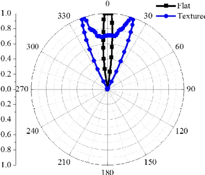
To understand how the scattering light capability of the flexible textured and flat PDMS films varies in the far-field pattern, we first measured the angle-dependent intensity of transmittance by bidirectional transmittance distribution function (BTDF) system with an incident light of 380 nm and ultraviolet-visible spectrophotometer. The view angle of the flexible textured PDMS film at the full-width at half-maximum was enlarged from 12° to 48° compared with the flat PDMS film, which could be attributed to the increased light scattering by the textured structure as shown in Fig. 3. As the results, the introduction of the flexible textured PDMS film can deflect the photons in much wider angle and lengthen the traveling distance in the cell, which implies higher possibility of getting absorbed.
Figure 3. The measured angular-dependent intensity of transmittance in flat/textured PDMS structures.
This effect can be readily seen in standard solar cell response. Fig. 4 shows the photovoltaic current density-voltage (I–V) characteristics of the GaAs solar cell with and without flexible textured PDMS film and the conventional SiO2 AR
coated GaAs solar cell by a class-A solar simulator with a xenon flash tube of IEC 904–9 standard. The GaAs solar cell with textured PDMS layer can effectively enhance the short-circuit current density from 22.91 to 26.54 mA/cm2 and the
power conversion efficiency from 18.28 to 21.43 %, corresponding to a 17 % enhancement compared to one without textured PDMS of GaAs solar cell. The open-circuit voltage (Voc) and the fill-factor (FF) in GaAs solar cell exhibit
negligible change, because the textured PDMS film was pasted up on the surface of GaAs solar cell and did not interfere with the diode operation. When compared with the conventional SiO2 ARC of GaAs solar cell, the textured PDMS cell
A
-Figure 4. Photovoltaic I–V characteristics of textured PDMS, No textured PDMS, and ARC of GaAs solar cells. The inset figure shows I-V characteristics of conventional and GQB LEDs.
To understand more thoroughly on the interaction of the textured PDMS with photons into the GaAs solar cell, we measured the spectral response of the external quantum efficiency (EQE). Fig. 5. shows the external quantum efficiency (EQE) as function of illumination wavelength for all three types of solar cells (with textured PDMS, with SiO2 ARC, and
without any coating), and the Fig. 6. shows reflectance spectra taking by an integrating sphere at the normal incidence of light. From EQE spectrum, the universal enhancement of with textured PDMS of GaAs solar cell is exhibited in the range from 320nm to 900nm, and the curves of textured PDMS and conventional SiO2 ARC of GaAs solar cell crisscross
at 550nm, which marks the rise of the single AR layer’s reflectance. The sample with textured PDMS, on the other hand, exhibits a universal reduction of reflectance, even beyond 550nm, and thus possesses a higher EQE. According to Fig. 6., the GaAs solar cell with textured PDMS film can offer a superior anti-reflective property in the range of wavelength from 360 nm to 1000 nm, compared with the cell without textured PDMS film, and this result agrees with measurement of EQE. The reduction of reflectance means more photons can get into the devices due to suitable refractive index of textured PDMS film (n~1.42) and the increase of light scattering due to the introduction of the textured PDMS; hence, more carriers can be generated, and an increase of photocurrent accordingly. From these experiments, we could found the introduction of textured PDMS film on GaAs solar cell surface brings several advantages: first is the refractive index gradient; second is the increase of light scattering at the surface; third is a simple implementation. All these effects can greatly improve the short-circuit current density with our conventional GaAs-based solar cells. With this way, the cost of device could be effectively reducing and replace conventional SiO2 ARC of solar cell.
Figure 5. Measurement of External quantum efficiency of textured PDMS, No textured PDMS, and ARC of GaAs solar cells.
Figure 6. The inset figure shows measured reflectance of textured PDMS, No textured PDMS, and ARC of GaAs solar cells.
CONCLUSIONS
In conclusion, we successfully improve power conversion efficiency by combining a flexible textured PDMS film with GaAs solar cell. Especially, it is noticeable that the textured PDMS film can significantly enhance short-circuit current density under air mass 1.5 global illuminations. The main mechanism of the enhancement can be attributed to anti-reflection and light scattering. Consequently, the overall power conversion efficiency is enhanced by 17% and 1.7%, when compared to the cell without textured PDMS film and conventional ARC cell, respectively. Furthermore, the angle-dependent intensity of transmittance in flexible flat PDMS and textured PDMS films by BTDF system was
measured to confirm that the view angle of the full-width at half-maximum was enlarged from 12° to 48°. Finally, we believe this technology shall be a great candidate for next generation of highly efficient and low-cost photovoltaic devices.
ACKNOWLEDGMENTS
This work is founded by National Science Council in Taiwan under grant number NSC 99-2120-M- 006-002 and NSC-99-2120-M-009-007. C. C. Lin would like to thank the financial support of National Science Council in Taiwan through the grant number: NSC101-3113-E-110-006-. The authors would also like to thank Prof. Shing-Chung Wang of NCTU for his help and support.
Reference
[1] R. R. King, D. C. Law, K. M. Edmondson, C. M. Fetzer, G. S. Kinsey, H. Yoon, R. A. Sherif, and N. H. Karam, Applied Physics Letters 90 (18) (2007).
[2] P. C. Yu, C. H. Chang, C. H. Chiu, C. S. Yang, J. C. Yu, H. C. Kuo, S. H. Hsu, and Y. C. Chang, Advanced Materials 21 (16), 1618 (2009).
[3] W. Guter, J. Schone, S. P. Philipps, M. Steiner, G. Siefer, A. Wekkeli, E. Welser, E. Oliva, A. W. Bett, and F. Dimroth, Applied Physics Letters 94 (22) (2009).
[4] Y. A. Chang, Z. Y. Li, H. C. Kuo, T. C. Lu, S. F. Yang, L. W. Lai, L. H. Lai, and S. C. Wang, Semiconductor Science and Technology 24 (8) (2009).
[5] M. A. Tsai, P. C. Tseng, H. C. Chen, H. C. Kuo, and P. C. Yu, Optics Express 19 (1), A28 (2011). [6] J. A. Dobrowolski, D. Poitras, P. Ma, H. Vakil, and M. Acree, Applied Optics 41 (16), 3075 (2002). [7] Y. Inomata, K. Fukui, and K. Shirasawa, Solar Energy Materials and Solar Cells 48 (1-4), 237 (1997). [8] E. Y. Wang and K. A. Pandelisev, Journal of Applied Physics 52 (7), 4818 (1981).
[9] C. C. Lin, H. C. Chen, Y. L. Tsai, H. V. Han, H. S. Shih, Yi. A. Chang, H. C. Kuo and P. Yu, Optics Express 20 (20), A319 (2012).
[10] H. C. Chen, C. C. Lin, H. W. Han, Y. L. Tsai, C. H. Chang, H. W. Wang, M. A. Tsai, H. C. Kuo, and P. C. Yu, Optics Express 19 (19), A1141 (2011).
[11] P. C. Tseng, P. C. Yu, H. C. Chen, Y. L. Tsai, H. W. Han, M. A. Tsai, C. H. Chang, and H. C. Kuo, Solar Energy Materials and Solar Cells 95 (9), 2610 (2011).
[12] C. H. Chiu, P. C. Yu, H. C. Kuo, C. C. Chen, T. C. Lu, S. C. Wang, S. H. Hsu, Y. J. Cheng, and Y. C. Chang, Optics Express 16 (12), 8748 (2008).
[13] C. H. Chang, P. Yu, and C. S. Yang, Applied Physics Letters 94 (5) (2009).
[14] K. Sato, M. Shikida, T. Yamashiro, M. Tsunekawa, and S. Ito, Sensors and Actuators a-Physical 73 (1-2), 122 (1999).