Fabrication and characterization of spherical polycrystalline
diamond emitter arrays
Chia-Fu Chen*, Wen-Hsien Huang
Institute of Materials Science and Engineering, National Chiao Tung University, Hsinchu 30050, Taiwan
Abstract
In this work, a high density of spherical polycrystalline diamond field emitter arrays (SPD-FEAs) were fabricated, using microwave plasma chemical vapor deposition (MPCVD) method. Results obtained from the current-voltage (Ie-Va) characteristics indicate that the
impurities heavily influence electron emission. In addition, the emissions current of the phosphorus-doped SDP-FEAs appears to be 25 times larger than the boron-doped and 120 times larger than the undoped SPD-FEAs.1997 Elsevier Science S.A.
Keywords: Diamond; Field emitter array; Emission current; Microwave plasma chemical vapor deposition
1. Introduction
Field emitter arrays fabricated with advanced micro-machining technology have received extensive interest as a highly promising electron source for vacuum microelec-tronics devices.
However, a ‘superior’ material deemed appropriate for such emitters has not yet been identified. To achieve low voltage and high efficiency for cold cathode operation, the surface work function of a field emitter should be minimized as much as possible. In addition, emission stability is also a critical issue for practical applications. Sharp silicon micro-tips, although highly attractive for field emitter arrays, are limited by a high work function and low electron conduc-tivity. Such limitations can hopefully be minimized using a surface coated with other materials. Hence, many investiga-tions have examined the surface of silicon micro-tips coated with various materials to enhance their emission efficiency and stability [1,2]. These studies focused primarily on metal coatings. Recent interest has concentrated on the feasibility of applying CVD diamond films as the electron emitter or cold cathode material in lieu of diamond’s unique electrical properties. As expected, diamond films is one of the stron-gest candidate materials owing to the following reasons: (a) hydrogenated-(111) diamond has a negative or at least an extremely small electron affinity [3], i.e. an extremely low effective work function, (b) diamond is one of the most chemically and physically stable materials in addition to
having the highest thermal conductivity (20 W/cm-°C) [4,5] among all other materials, and (c) a high breakdown threshold (107 V/cm) and a rather large high-field electron velocity (2.7×107 cm/s) would enhance the maximum emission current which is limited by current saturation [6]. Hence, attempts have been made to fabricate low-field diamond field emitter arrays [7].
In this study, we have developed and characterized a new fabrication technology involving a high density of spherical polycrystalline diamond field emitter arrays (SPD-FEAs) using a microwave plasma chemical vapor deposition (MPCVD) method. The phosphorus-doped SPD-FEAs and the boron doped SPD-FEAs are compared in terms of their fabrication capabilities. In addition, the effects of diamond dopant on field emission properties are discussed. More-over, scanning electron microscopy (SEM), X-ray diffrac-tion (XRD), Raman spectroscopy and secondary ion mass spectroscopy (SIMS) results confirm the existence of depos-ited diamond (SPD-FEAs).
2. Experimental details
The starting substrates were polished p-type, (100) oriented Si wafers having a resistivity of 10–20Q-cm. The wafers were cleaned in acetone, methanol, and DI-water and then dried with nitrogen gas. By using pyrogenic steam, the cleaned silicon wafer was thermally oxidized at 1180°C for 120 min to attain a 1 mm thick SiO2layer. Next, the SiO2 layer was lithographically patterned and chemically etched
0040-6090/97/$17.00 1997 Elsevier Science S.A. All rights reserved P I I S 0 0 4 0 - 6 0 9 0 ( 9 7 ) 0 0 6 7 1 - 8
* Corresponding author. Tel.: +886 35 731898; fax: +886 35 723811, e-mail: [email protected]
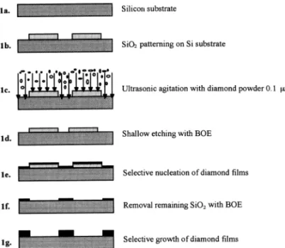
in a buffered HF/NH4F/H2O (3:6:10) solution. The layer was then masked with 1 mm SiO2, with the patterns having a square-shape of 2 mm width. The distance between squares was 4 mm. The 50×50 square-pattern was 0.3×0.3 mm in area. After masking, these patterns were RIE etched to a 1 mm depth. Next, the sample was ultrasonically agitated in DI-water containing 0.1 mm diamond powder for 10 min. The sample was then dipped in a buffered HF solution for 20–30 s to etch the SiO2layers to about 50–60 nm in depth. After nucleating diamond for 10 min in the chamber, the sample was again dipped in buffered HF to remove the remaining SiO2. Finally, the substrate was placed into the chamber in order to selectively deposit diamond films. Fig. 1 depicts the above process.
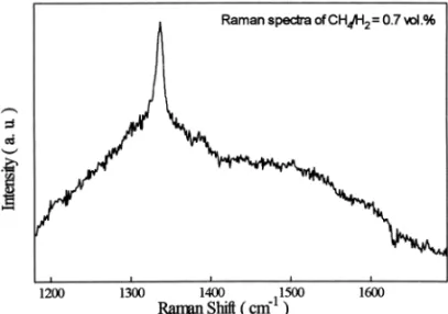
The reactant gases were the commercial grade H2 and high purity (99.998%) CH4. The results presented here were obtained at a total pressure of 3.3 kPa (25 Torr). The gas mixture used was CH4-H2, having a ratio of 3.8 vol.% during the nucleation step and 0.7 vol.% during growth. The microwave generator was maintained at 400 W. An optical pyrometer was used to monitor the substrate temperature, which was maintained at approximately 850°C. The dura-tion of the nucleadura-tion and the growth were 10 min and 1–1.5 h, respectively. Fig. 2 displays the excellent selective-area growth of SPD-FEAs.
3. Results and discussion
Fig. 2 presents an SEM micrograph of selective-area deposition of undoped SPD-FEAs. The Raman spectrum in Fig. 3 reveals the undoped SPD-FEAs quality. According to the Raman spectrum, each small spherical polycrystalline diamond has a characteristic peak; however, its position is slightly shifted from that of natural diamond (1332.5 cm−1) because of internal stress in the film. The strong peak
appearing at 1330 cm−1can be found in diamond, whereas the broader hump centered around 1400–1500 cm−1denotes carbon disorder. Fig. 4 depicts the I-V characteristics. As this figure indicates, the emission current (Ie) is 0.99 mA for the applied voltage (Va) of 1100 V.
Herein, the doping was achieved with B(OCH3)3 and P(OCH3)3 as dopant sources. The dopant flow rates were all 5 sccm. Figs. 5 and 6 display the morphologies of these impurity doped SPD-FEAs.
The Raman spectra in Figs. 7 and 8 reveal that the boron doped and phosphorus doped SPD-FEAs and have two interesting features:
1. A sharp peak appears at ~1330 cm−1, due to the characteristic line of diamond, and
2. Two broad peaks appear at ~1330 and 1550 cm−1, due to the characteristic line of diamond-like carbon [8].
The peaks of these impurity doped diamond SPD-FEAs are slightly shifted from the natural diamond peak (1332.5 Fig. 1. Procedure for selective-area deposition on the substrate
pretreat-ment.
Fig. 2. The SEM of the selective-deposition undoped diamond films at the 2 mm-square substrate.
cm−1). In addition, a slight broadening of the 1332.5 cm−1 peak occurs when these dopant sources are introduced into the reactant gases. This occurrence can be accounted for by the lattice strain caused by the dopants [9,10]. The broad
peaks appearing at 1550 cm−1reveal a reduced domain size for the diamond, thereby suggesting a loss in the diamond’s structural perfection. Restated, the methyl radicals (CH3), i.e. a precursor of diamond growth, might decrease the etch-Fig. 3. The Raman spectra of the selective-area undoped diamond films.
Fig. 4. The Ie-Vacurve of selective-area undoped diamond films at 2
mm-square substrate.
Fig. 5. SEM image of the selective-area boron doped diamond films at 2 mm-square-pattern substrate.
Fig. 6. SEM image of the selective-area phosphorous doped diamond films at 2 mm-square-pattern substrate.
Fig. 7. The Raman spectra of the B-doped diamond films.
ing rate and increase in the amount of amorphous carbon or graphite remaining in the doped films [11].
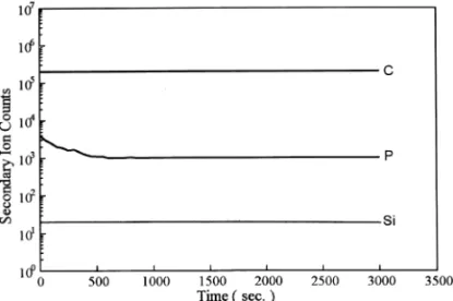
Figs. 9 and 10 present the secondary ion mass spectro-metry (SIMS) depth profile analysis of the doped SPD-FEAs. According Figs. 9 and 10, the depth distribution of boron and phosphorus is quite uniform in the measured regions (up to 3000 s, about 1 mm in depth). Also, the boron and phosphorus atoms can uniformly distribute in the SPD-FEAs by using tri-methyl borate and tri-methyl phosphate as the dopant sources in the CH4-H2gas mixtures. Figs. 11 and 12 illustrate the I-V characteristics. From the
I-V characteristics, the values of (Ie) of the doped SPD-FEAs seem to be larger than the undoped ones. The (Ie) of the boron doped SPD-FEAs is around 24.74 mA, and the (Ie) of the phosphorus doped is 119.32 mA. Our previous works [8,9] suggested that the boron atoms are located in the sub-stitutional sites and the phosphorus atoms are nearly in the inactive sites (e.g. grain boundaries and clustering sites) of the doped SPD-FEAs. Herein, the emission current’s value is determined by the number of electrons. Moreover, the phosphorus atoms can supply more electrons because the number of valence electrons is 5. Boron atoms only contri-bute holes because the number of valence electrons is 3.
Therefore, that the (Ie) of the phosphorus doped SPD-FEAs is larger the than (Ie) of the boron doped SPD-FEAs is apparent.
4. Conclusion
The results of this study demonstrate that impurities heavily influence the emission current (Ie) efficiency. The
Ie of phosphorus-doped SPD-FEAs and the Ie of boron-doped SPD-FEAs are 120 and 25 times, respectively, greater than that of the undoped SPD-FEAs. Phosphorus atoms not only tend to migrate to inactive areas (e.g. grain boundaries and clustering sites) but also provide more valence electrons. Therefore, the phosphorus doped SPD-FEAs yield more emission current than the boron-doped and the undoped SPD-FEAs.
Acknowledgements
The authors would like to thank the National Science Council of the R.O.C. for financial support of this work under contract No. NSC-85 2216-E-009-013.
Fig. 9. SIMS depth profile of B-doped diamond films. B(OCH3)3=5
(sccm).
Fig. 10. SIMS depth profile of P-doped diamond films. P(OCH3)3=5
(sccm).
Fig. 11. The Ie-Vacurve of selective-area B-doped diamond films at 2
mm-square substrate.
Fig. 12. The Ie-Vacurve of selective-area P-doped diamond films at 2
References
[1] R.B. Marcys, T.S. Ravi, T. Gmitter, K. Chin, W.J. Orvis, D.R. Ciarlo, C.E. Hunt and J. Trujillo, Appl. Phys. Lett., 56 (1990) 236. [2] H.H. Busta, R.R. Shadduck and W.J. Orvis, IEEE Trans. Electron.
Dec., 36 (1989) 2679.
[3] V.V. Zhirnow and E.I. Givargizov, J. Vac. Sci. Technol. B, 12 (1994) 633.
[4] F.J. Himpsel, J.A. Knapp, J.A. VanVechten and D.E. Eastman, Phys. Rev. B, 20 (1979) 624.
[5] P. Vandaine and R. Meer, IEEE IEDM (1991) 197.
[6] K. Okano, K. Hoshino, M. Lida, S. Koizumi and T. Inuzuka, Appl. Phys. Lett., 64 (1994) 2742.
[7] S. Matsumoto, Y. Sato, M. Tsutsumi and N. Setaka, J. Mater. Sci., 17 (1982) 3106.
[8] D.S. Knight and W.B. White, J. Mater. Res., 4 (1989) 4385. [9] N. Setaka, Hyomen Gijutsu, 22 (1984) 110 (in Japanese).
[10] K. Nishimura, K. Das, J.T. Glaass, K. Kobashi and R.J. Nemanich, Proc. NATO Adv. Res. Workshop on Phys. and Chem. of Carbides, Nitrides and Borides, Manchester, UK, 1989.
[11] C.F. Chen, S.H. Chen, T.M. Hong and T.C. Wang, Thin Solid Films, 248 (1994) 149.