Metalorganic chemical vapor deposition of InGaN layers on ZnO substrates
Shen-Jie Wang, Nola Li, and Eun-Hyun Park
School of Electrical and Computer Engineering, Georgia Institute of Technology, Atlanta, Georgia 30332-0250, USA
Siou-Cheng Lien and Zhe Chuan Fenga兲
Institute of Photonics and Optoelectronics and Department of Electrical Engineering, National Taiwan University, Taipei, Taiwan 106-17, Republic of China
Adriana Valencia and Jeff Nause
CERMET Inc., 1019 Collier Road, Atlanta, Georgia 30318, USA Ian Fergusonb兲
School of Electrical and Computer Engineering, Georgia Institute of Technology, Atlanta, Georgia 30332-0250, USA
共Received 30 July 2007; accepted 1 October 2007; published online 29 November 2007兲
InGaN layers have been grown on 共0001兲 ZnO substrates by metalorganic chemical vapor deposition utilizing a low temperature grown thin GaN buffer. Good quality InGaN films with a wide range of In composition were confirmed by high-resolution x-ray diffraction. Even at high indium concentrations no In droplets and phase separation appeared, possibly due to coherent growth of InGaN on ZnO. Photoluminescence showed broad InGaN-related emissions with peak energy lower than the calculated InGaN band gap, possibly due to Zn/O impurities diffused into InGaN from the ZnO substrate. An activation energy of 59 meV for the InGaN epilayer is determined. © 2007 American Institute of Physics.关DOI:10.1063/1.2817482兴
I. INTRODUCTION
ZnO is a wurtzite semiconductor with a small c-plane lattice mismatch of 1.8% compared to wurtzite GaN. InGaN, with a composition of 18% In, possesses a perfect lattice match with ZnO in the a-axis direction according to Vegard’s law and, hence, allows for the possible growth of InGaN layers without misfit dislocations.1,2ZnO has a similar ther-mal expansion coefficient with GaN which allows for almost zero thermal strain.3In addition, ZnO substrates are conduc-tive so they can be utilized in vertical structures allowing for multiple electrodes to be formed on both surfaces to further current spreading.4,5 Furthermore, ZnO can be wet-etched chemically and easily removed to allow for a thin GaN structure.6,7 Therefore, ZnO is an ideal alternative substrate for GaN and InGaN based devices compared to growth on sapphire or SiC. Previously, molecular beam epitaxy and pulse laser deposition techniques have been employed to re-alize the low temperature epitaxy of GaN-based materials on ZnO substrates.1,2,8
However, metalorganic chemical vapor deposition 共MOCVD兲 is currently the dominant growth technology for GaN-based materials and devices and there is a need to ex-plore this technique for ZnO substrates. It is well known that the decomposition of ZnO substrates leads to an increase in Zn and O diffusion during high temperature growth, which can result in poor epitaxial growth and degrade the film quality.1,2,8This issue also has been demonstrated by
second-ary ion mass spectrometry depth profile of the GaN/ZnO interface.9,10 Commercial MOCVD usually grows over 1000 ° C for GaN on sapphire substrates, which makes it difficult for MOCVD growth of GaN and InGaN on ZnO substrates. So far, only one group has reported the MOCVD growth of GaN on ZnO, which showed x-ray diffraction 共second order兲 and photoluminescence 共PL兲 peaks from GaN layer.11
In this study, the growth of InGaN layers on共0001兲 ZnO substrates by MOCVD is reported. The grown InGaN layers contained high In composition in the range of 17% – 27%, which are suitable for typical InGaN multiple quantum wells 共MQWs兲 light emitting diode device applications. It is dem-onstrated that this achievement is the use of a low tempera-ture thin GaN buffer layer to grow InGaN films on ZnO substrates.
II. EXPERIMENT
InGaN films were grown on the Zn face of共0001兲 ZnO substrates by MOCVD in a modified commercial rotating disk reactor with dual injector blocks. A low temperature GaN buffer layer was grown at 530 ° C with a thickness of about 30 nm using trimethylgallium and ammonia as the gallium and nitrogen sources, respectively. Following the buffer, InGaN layers of about 70 nm thick were grown at temperatures ranging from 680 to 720 ° C by introducing trimethylindium and triethylgallium into the reactor. N2 car-rier gas was used during the whole growth process in order to avoid etching of the ZnO surface. By varying the growth temperature, the In concentration and growth rate of the in-vestigated films were varied from 17% to 27% and 0.16 to 0.2 m/h, respectively. The structure and In composition of a兲Also at School of Electrical and Computer Engineering, Georgia Institute
of Technology 共sabbatical visiting兲. Electronic mail: [email protected].
b兲Electronic mail: [email protected].
JOURNAL OF APPLIED PHYSICS 102, 106105共2007兲
0021-8979/2007/102共10兲/106105/3/$23.00 102, 106105-1 © 2007 American Institute of Physics
the InGaN layers were characterized by high-resolution x-ray diffraction 共HRXRD兲 using a Philips X’Pert Pro MRD dif-fractometer. Optical properties were measured by room tem-perature and temtem-perature-dependant PL. The field-emission scanning electron microscopy 共FE-SEM兲 was utilized to evaluate the surface morphologies of the InGaN films. III. RESULTS AND DISCUSSION
Figure 1 shows HRXRD共first order兲 2/ scans from three samples, each consisting of two well-separated peaks from the ZnO substrate and InGaN layers, respectively. The concentration of In from the InGaN layer was calculated by the shift of the 共0002兲 InGaN peak position relative to the 共0002兲 ZnO peak position 共set at 0 arcsec兲 via Vagard’s law. The variation of In incorporation in the InGaN layers was adjusted by changing growth temperature. The InGaN films showed single crystal diffraction peaks by 2/ scans cor-responding to the 17%, 23%, and 27% In content with the samples grown at 720, 700, and 680 ° C, respectively. All XRD patterns revealed the small shoulder close neighbor on the right of the ZnO peaks which might be from the diffrac-tion of the GaN buffer layer. Remarkably, only InGaN and ZnO peaks appeared in all the samples and no extra peaks were observed even in samples with composition as high as 27%. This meant no In droplets or phase separation were detected by XRD from the InGaN layers. In addition, all samples have been examined by FE-SEM with mirrorlike InGaN surfaces and no evidence of In droplets on the sur-face, as shown in Fig. 2.
For InGaN grown on thick GaN coated sapphire, the phase separation was widely reported for high In composi-tion, caused by spinodal decomposition. However, for our InGaN films grown on the ZnO substrate, In droplets or phase separation were not detected by HRXRD, in contrast to the earlier cases.12,13 From theoretical calculation and ex-perimental observation, biaxial strain in the epilayer is help-ful in suppressing the phase separation in InGaN materials.14,15 Phase separation easily occurs when the In-GaN layer starts to relax due to compressive strain from thick GaN/sapphire. Here, the observed suppression of phase separation in the film is believed to be due to a higher strain
state of InGaN with high In content compared with the InGaN/thick GaN/sapphire materials system. The InGaN layer may stay completely strained on the thin GaN buffer, which is coherently grown on the underlying ZnO, with high In composition, since InGaN consisting of 18% In is exactly lattice matched with ZnO. As a result, a higher strain state in InGaN films with a high In concentration will be provided by ZnO compared with those grown on thick GaN/sapphire to retard the phase separation. This discrepancy is possibly caused from the different strain relaxation mechanisms in thin GaN/ZnO and thick GaN/sapphire substrate.
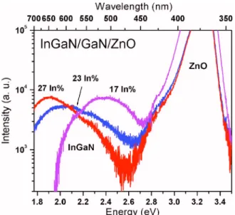
Figure3shows the room temperature PL spectra of these three samples. The emissions from the InGaN layers with different In compositions and from the ZnO substrate are observed. For the samples with an In composition of 17%, 23%. and 27%, the emission peaks were observed at 2.4, 2.1, and 1.9 eV, respectively. Assuming the 70 nm InGaN layers were strained and employing the reported band gap expres-sion, Eg = 3.42−共0.65兲x−3.4159x共1−x兲,16 where x is the composition of In, the band edge emission energy can be calculated if the In concentration is known. Using the x共In兲 values of 17%, 23%, and 27% from HRXRD measurements in Fig.1, the calculated PL peak energies of 2.8, 2.6, and 2.5 eV are obtained, respectively, which are quite different from
FIG. 1.共Color online兲 HRXRD 2/scan of InGaN layers with different In composition grown on ZnO substrates by MOCVD.
FIG. 2. 共Color online兲 FE-SEM image of InGaN surface grown on ZnO substrates at 700 ° C by MOCVD.
FIG. 3. 共Color online兲 Room temperature PL spectra of InGaN films with different In composition grown on ZnO substrates by MOCVD.
106105-2 Wang et al. J. Appl. Phys. 102, 106105共2007兲
the experimental PL results in Fig. 3. Each calculated PL peak for the InGaN layer shifts from the experimental spec-tral PL peak by about 0.4–0.6 eV. The lower energy PL emis-sions may be due to Zn and O diffusion from ZnO into the InGaN layers forming impurity levels inside the band gap emitting light with energy lower than the InGaN energy gap. It also has been observed that intentionally Zn doped InGaN shows values between 0.4 and 0.5 eV lower than calculated and experimental band gap energy of InxGa1−xN without Zn doping.17 A high density diffusion of Zn and O impurities into InGaN might also be a contributing factor to the broad full width half maximum seen in PL.
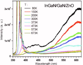
To further verify the InGaN related PL emission, temperature-dependant PL was done over a wide range of temperature from 80 to 673 K for the InGaN film grown at 700 ° C, with x共In兲 of 23%, Fig.4. The variation in intensity of InGaN 共below 630 nm兲 with temperature is seen in this region. It shows that the PL intensity decreases with an in-crease in temperature, slowly at the low temperature region of 80–300 K but rapidly at the high temperature region of 373–673 K. Figure 5 exhibits the Arrhenius plot of InGaN-related PL peak intensity versus temperature in the range of 80–673 K. Best fitting leads to an activation energy, Ea, of about 59 meV for InGaN with 23% In content. Smith et al.18
report an Ea= 56 meV for the InxGa1−xN epilayer with x = 0.12 and Teo et al.19report on In0.2Ga0.8N MQWs with an
Eavalue of 63 meV. The data reported in this paper are close to the earlier reported values in literature.
IV. CONCLUSIONS
In summary, MOCVD technology has been employed for the epitaxial growth of InGaN layers on共0001兲 ZnO sub-strates. This was achieved with the use of a low temperature grown thin GaN buffer layer. Good quality InGaN films with a range of high In composition of 17% – 27%, as determined by high-resolution x-ray diffraction, have been obtained with growth temperatures of 680– 720 ° C. The InGaN films show no In droplets or phase separation. The lack of phase sepa-ration has been attributed to the higher strain state in InGaN epilayers grown on ZnO substrates. Room temperature PL data for all InGaN films show a strong emission band from ZnO and broad InGaN-related emissions with the peak en-ergy varying with In composition. Peak enen-ergy values of the broad emissions are measured to be less than the calculated InGaN band gap by 0.5± 0.1 eV. These InGaN-related emis-sions are most likely due to recombinations involving Zn/O impurities in InGaN due to the Zn/O diffusion from the ZnO substrate. Temperature-dependent PL measurements, 80–673 K, obtained an activation energy of 59 meV for the InGaN epilayer.
1A. Kobayashi, J. Ohta, and H. Fujioka, J. Appl. Phys. 99, 123513共2006兲. 2G. Namkoong, S. Burnham, K. Lee, E. Trybus, W. A. Doolittle, M.
Lo-surdo, P. Capezzuto, G. Bruno, B. Nemeth, and J. Nause, Appl. Phys. Lett. 87, 184104共2005兲.
3F. Hamdani, M. Yeadon, D. Smith, H. Tang, W. Kim, A. Salvador, A. E.
Botchkarev, J. M. Gibson, A. Y. Polyakov, M. Skowronski, and H. Morkoc, J. Appl. Phys. 83, 983共1998兲.
4G. H. B. Thompson, Physics of Semiconductor Laser Devices 共Wiley,
Chichester, 1980兲, p. 307.
5A. Zukauskas, M. S. Shur, and R. Gaska, Introduction to Solid-State
Lighting共Wiley, New York, 2002兲, p. 75.
6W. S. Wong, T. Sands, N. W. Cheung, M. Kneissl, D. P. Bour, P. Mei, L.
T. Romano, and N. M. Johnson, Appl. Phys. Lett. 77, 2822共2000兲.
7S. C. Hsu and C. Y. Liu, Electrochem. Solid-State Lett. 9, G171共2006兲. 8X. Gu, M. A. Reshchikov, A. Teke, D. Johnstone, H. Morkoc, B. Nemeth,
and J. Nause, Appl. Phys. Lett. 84, 2268共2004兲.
9G. Popovici, W. Kim, A. Botchkarev, H. Tang, H. Morkoc, and J.
So-lomon, Appl. Phys. Lett. 71, 23共1997兲.
10T. Suzuki, C. Harada, H. Goto, T. Minegishi, A. Setiawan, H. J. Ko, M. W.
Cho, and T. Yao, Curr. Appl. Phys. 4, 643共2004兲.
11R. Paszkiewicz, B. Paszkiewicz, R. Korbutowicz, J. Kozlowski, M.
Tlac-zala, L. Bryja, R. Kudrawiec, and J. Misiewicz, Cryst. Res. Technol. 36, 971共2001兲.
12N. A. El-Masry, E. L. Piner, S. X. Liu, and S. M. Bedair, Appl. Phys. Lett.
72, 40共1998兲.
13Z. C. Feng, T. R. Yang, R. Liu, and T. S. A. Wee, Mater. Sci. Semicond.
Process. 5, 39共2002兲.
14A. Tabata, L. K. Teles, L. M. R. Scolfaro, J. R. Leite, A. Kharchenko, T.
Frey, D. J. As, D. Schikora, K. Lischka, J. Furthmüller, and F. Bechstedt, Appl. Phys. Lett. 80, 769共2002兲.
15S. Y. Karpov, MRS Internet J. Nitride Semicond. Res. 3, 16共1998兲. 16C. A. Parker, J. C. Roberts, S. M. Bedair, M. J. Reed, S. X. Liu, N. A.
El-Masry, and L. H. Robins, Appl. Phys. Lett. 75, 2566共1999兲.
17S. Nakamura, J. Cryst. Growth 145, 911共1994兲.
18M. Smith, G. D. Chen, J. Y. Lin, H. X. Jiang, M. Asif Khan, and Q. Chen,
Appl. Phys. Lett. 69, 2837共1996兲.
19K. L. Teo, J. S. Colton, P. Y. Yu, E. R. Weber, M. F. Li, W. Liu, K. Uchida,
H. Tokunaga, N. Akutsu, and K. Matsumoto, Appl. Phys. Lett. 73, 1697 共1998兲.
FIG. 4. 共Color online兲 Temperature-dependent PL spectra 共80–673 K兲 of InGaN film grown on the ZnO substrate at 700 ° C.
FIG. 5. PL intensity vs temperature共80–673 K兲 of the InGaN layer.
106105-3 Wang et al. J. Appl. Phys. 102, 106105共2007兲