esign and Implementation
of
a
High Speed Parallel Architecture
for
ATM UNIt
Wen-Yu Tseng, Chin-Chou Chen, David
S. L.
Wei* and Sy-Yen
Kuo
Department of Electrical Engineering
National Taiwan University
Taipei, Taiwan, R.O.C.
*School of Computer Science and Engineering
The
University
of
A i m
Fukushima, 965-80 Japan
Abstract
In t h i s p a p e r , a parallel architecture is proposed t o support t h e operations described in t h e I T U - T R e c - o m m e n d a t i o n 1.432
(B-ISDN
u s e r - n e t w o r k i n t e r f a c e -Physical layer specification).
It
i s r a t h e r difficult t o p e r f o r m t h e s e operations o n abit
serial architecture at a high rate. T h i s paper demonstrates h o w these tasks c a n be achieved by m e a n s of parallelism. F i r s t , w e de- scribe t h e u s e r - n e t w o r k i n t e r f a c e s in general and their physical layer properties. T h e n a parallel architecture i s proposed w i t h a general t r a n s l a t i o n m e t h o d w h i c h converts t h e serial operation into t h e parallel o n e . T h e application of the parallel architecture o n each f u n c - tion i s also depicted a n d t h e s y s t e m h a s been realized in hardware using CMOS technology.1
Introduction
There is widespread activity in the telecommu- nications industry t o provide broadband video and d a t a services. Broadband Integrated Services Digi- tal Networks enable high d a t a transfer, video confer- ence, video telephony and any other broadband ser- vices based on asynchronous transfer mode (ATM). In ATM, all information t o be transmitted is packed in fixed-size (53 octets) cells. These cells have a 48 octet information field and a 5 octet header.
User Network Interface (UNI), which is defined in ITU-T Recommendation 1.432 [2], defines the func- tions of interactions between users and networks. It contains error control and scrambling/descrambling functions. Two interface types were standardized in [2]: the SDH-based interface and the cell-based inter- face. For the SDH-based interface [3, 4, 51, the ATM cell stream is mapped into the byte frame. The SDH- based
B-ISDN UN1 implementation has the advantage
!This research was supported by the Telecommunication Laboratory, Taiwan, R.O.C., under the contract TL-847205.Cell
Ue,inenl,,r
S I P 0 Ue~cminbler R
Figure 1: Bit-Serial Architecture of ACUNI Chip.
of full compatibility between the user-network inter- face and the network-node interface a t the expense of the large overhead capacity in the frame. While the cell-based UNI, on which no multiplexing frame structure is imposed, has the advantage of high speed features and efficiency, the cell-based interface itself is not yet fully defined, e.g., coding and allocation of OAM functions are not sufficiently clear. Therefore, the cell-based interface is adopted in the implementa- tion of the chip design. This chip is expected to find important applications in ATM cells multiplexing and demultiplexing prototype a s well as in many broad- band network systems, such as the link termination of user-network interface, and interconnection interfaces of the ATM multistage switches.
At the physical bit level the B-ISDN user-network interface has a bit rate of 155.52 Mbps or 622.08 Mbps. T h e original architecture of the ATM cell-based user- network interface (ACUNI) chip in a bit-serial opera- tion is first proposed in [6] as shown in Fig. 1. However, it was shown via simulation and implementation in [6] that this bit-serial architecture can not achieve such high bit rates directly. Thus, a parallel architecture is proposed t o accomplish this task.
This paper is organized as follows. The principles of the parallel architecture as well as a general transla- tion method are presented in Sec. 2. The application of the the octet-parallel architecture on each function
is depicted in Sec. 3. Sec. 4 shows the parallel archi- tecture and the fabrication d a t a of our ACUNI chip. Finally, the conclusioln is given in Sec. 5.
2
Principles
of
Parallel Architecture
As described in the previous section, two different bit rates are defined; one is 155.52 Mbps and the other is 622.08 Mbps. It is rather difficult t o perform those operations on a bit-serial architecture a t such a high bit rate of 155.52 Mbps by today's CMOS technology, not to mention the rake of 622.08 Mbps [6]. Therefore, we propose a parallel architecture to support the op- erations documented in the ITU-T Recommendation 1.432.The parallel architecture is effective in that the de- crease in the operating frequency is significant. Take the interface of 622.08 MHz for example, the operat- ing frequency is reduced down t o less than 80 MHz if performed octet by octet. As a consequence, this architecture enables ithe design of the user-network in- terface by means of field programmable gate arrays or standard cells. In fact, we do use standard cells$ t o facilitate the design flow.
The only drawback in the parallel architecture is the hardware overhead because more combinational logic gates are required than in the serial architec- ture. However, since our objective is t o achieve the high speed ATM cell-based user-network interface, the additional small area overhead is insignificant and ac- ceptable. Besides, power dissipation may not neces- sarily increase with the total area as the operating fre- quency has been lowered down. In most cases, power dissipation can be further reduced with optimization of combinational logic under the parallel architecture.
2.1
Linear Feedlback Shift Register
A linear feedback; shift register [7] is a circuit con- sisting of D flip-flops and XOR gates with one or more feedback links. Linear feedback shift registers (LFSRs) are used extensively in many applications. Signature analysis, for example, is a compression technique based upon the concept of cycle redundancy checking (CR- C) [8] and is realized in hardware using linear feedback shift registers. In add.ition, HEC generation, cell delin- eation, scrambling/descrambling defined in the ITU-T Recommendation 1.432 can also be realized with LF- SRs. Before we discuss the details of the parallel ar- chitecture, some baclkground on the theory and oper- ations of LFSRs are necessary.
A linear circuit is a logic network constructed from the following basic components:
0 unit delays or D flip-flops;
0 modulo-2 adders or XOR gates;
0 modulo-2 scalar multipliers.
Such a circuit is considered t o be linear since it pre- serves the principle of superposition, i.e., its response t o a linear combination of stimuli is the linear combi- nation of the responses of the circuit to the individual stimulus.
In the following, we will first deal with a class of linear circuits, known as autonomous linear feedback shift registers that have no input except for clocks. We define the length 1 as the number of shift registers in autonomous L F S h and the state vector Q k as an
I-
vector representing the state of the shift registers at time
k,
i.e.,Q k
= ( q i , ~ ? z , * * * , q i ) ~ ,
(1) where qi,i
= 1 , 2 , .-,
I, denotes the value of the i-th register and the superscript means transpose.The state transition matrix, denoted by T I is de- fined as an
I
x l matrix representing the relationship between the state vectors Q k and Q k + l , or more specif- ically,Q k + i
T
* Q k . (2) The extent of parallelism, denoted by n, is defined as the multiple of the d a t a process at one time. Since the autonomous LFSRs has no inputs, it is not nec- essary t o process the d a t a and the autonomous LFSR just proceeds directly t o the n-th state. From Eq. (2),Q k + n =
T
'
'
a Q k .From Eq. ( l ) ,
where
In the above equation, T n e i , i = 1 , 2 , .
.
.,
k,
can be viewed as the response of the stimulus in each D flip- flop.Consider the case of LFSR with inputs. We define the sequence {xk} as the input of a LFSR in which Xk
is applied at time I C . The input can also be regarded as other stimuli, denoted by X , for LFSRs. The stimuli caused by the input in Fig. 2, for example, is '1101'.
Figure 2: An example input stimulus. By superposition theorem, the stimuli for the in- put should be included, or more specifically,
Qk+n = 41
.
Tnei
+
q 2.
T"e2+
. . .
+
41.
p e r+
Zk .T n W 1 X
+
Zk+1 'p w 2 x
+
' * '+
ak+n-2 ' T X+
Zk+n-l 'x.
(4)In the next section, we will explain the application of these formulas in detail.
Up to this point, it is assumed, for simplicity, that the LFSRs have no output. Now, the output shall be taken into account. We define the sequence {q} as the output sequence of LFSRs and the generating vector
W
as an I-vector representing the relationship between the state vectorQk
and the output sequence {zk}, or more specifically,Zk
= H * Q k .
(5)For a Mealy machine, the output zk is not only a func- tion of the present state but also a function of the present input xk. Since LFSRs preserve .the principle of superposition, Eq. (5) can be written as
zk = H * Q k
+
Xk..For a complete parallel architecture of LFSR, the out- put sequence { z k , & + I , .
. .
,
Zk+n-l} is also necessaryin addition to
Q k + % .
(6)
2.2
Other Sequential Circuits
So far as the nonlinear sequential circuit is con- cerned, there exists a similar method to convert the nonlinear circuit in serial mode into the one in parallel mode. Instead of deriving explicit equations, we briefly describe the general translation procedure. First, sup- pose that the state vector of the nonlinear sequential circuit is denoted by Q k and the input sequence is {Zk}. The next state & k + 1 can be obtained in terms
of
Qk
and x k . Then Q k + 2 can be obtained fromQ k + l
and expressed in terms of
Qk
and { Z k , Zktl}. Repeatthe above procedure until
Q k + n
represented in terms ofQk
and { x k , Zk+l,.. .
,
Zk+n-l} is obtained. Mean-while, the output sequence { Z k , Z k + l , ~ . ~ , Z k + n - l } Will
be calculated directly from the corresponding states of {Qk,Qk+l,...,QkSn-l}. Of course, the output sequence {zk, Zk+l,.
. .
,
Zk+n-l} itself should be ex-pressed in terms of
Qk
and {Zk, Zk+1,..
.
,
Zk+n-l}.In one word, the parallel architecture of the general sequential network is constructed based upon the fol- lowing results in terms of the state and the input sequence { x k l Zk+l,.
,
Zk+,-l}:e the next n-th state Q k + n ;
e the output sequence {Zk, zk+l,.
.
~ k + ~ - l } . The most important difference from LFSRs is that combination logic circuits after translation often be- come more complicated than those in LFSRs and op- timization is required to simplify the equations.3.
Applications
3.1
Scrambler
for Cell-Based
UN1
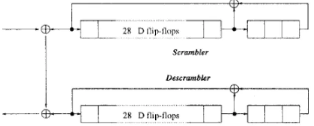
The distributed sample scrambler [9] is recom- mended for the cell-based user-network interface. It is a class of scrambler in which randomization of the transmitted d a t a stream is achieved by modulo-2 ad- dition of a pseudo random sequence. The pseudo ran- dom sequence polynomial is z31
+
zZ8+
1,
as shown inFig. 3. For our purpose, we choose t o skip 7 states and
Figure 3: Distributed Sample Scrambler
/
Descram- bler.
jump to every 8th state since the scrambler operation is desired to be performed in parallel on an octet of 8 bits. According t o Eq. (6), the output sequence is
zk+i = 928-i
+
q31-i+
Zk+i,i
= 0, 1,..
. 1 7 ,where q; is the value in the corresponding D flip-flop. While
Qk+n
in Eq. (4) can be obtained by the direct calculation of T", another short-cut method is adopted to simplify the calculation ofT".
The keypoint behind this method is that each flip-flop in
LF-
SRs can be treated separately and be combined later
by the superposition theorem. For example, the val- ue of the first (left-most) D flip-flop in Fig. 3 will bem o v e d to the 9th D flip-flop after 8 clock cycles, i.e., q$ is a function of 4 1 . Another example is that the value
of the 28th D flip-flop will be distributed to both the 5th and the 8th D flip-flops. The next state transition logic is:
4: = qii-20 4i+2!3
+
z k + 8 - i ,i
= 1 , 2 , ..
.
,8,q: = q i - 8 ,
i
= 9,10,.. .
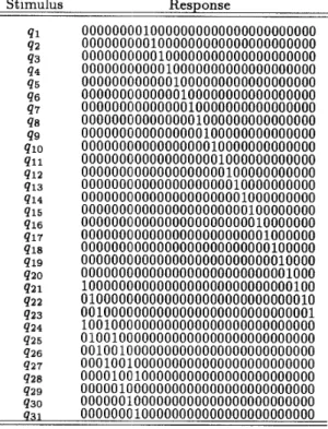
~ 31,All situations are listed in the form of the stimulus- response pair in Table 1. Note that in the parallelized distributed sample scrambler, the correction vector should be modified t o align on the octet boundary.
Table 1: Next State of Distributed Sample Scrambler in Parallel.
Stimulus Response
Figure 4: Self Synchronous Scrambler/Descrambler.
The output sequence { Z k , Z k + l ,
-
,
Zk+7} of thescrambler/descrambler is
z k + i = q43-i z k + i ,
i
=
0, 1,. . .
,
7,The next state transition logic is: q:
=
qi+35+
z k + 8 - i ,q: = q i - 8 ,
i
= 1,2,.. .
, 8 ,i
= 9,10,.. .
,43, The next-state table of the self synchronous scrambler in the form of stimulus-response pair, as depicted in the above subsection, is omitted for clarity.3.3
HEC
Generation
The header error control (HEC) is an 8-bit se- quence. It will be the remainder of the division (mod- ulo 2) by the generator polynomial x 8
+
z2+
z+
1 of the product z8 multiplied by the content of the head- er excluding the HEC field, t o which the fixed pattern 'OIOIOIOlywill be added. The HEC generator is shown in Fig. 5.Figure 5: HEC Generator.
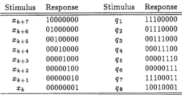
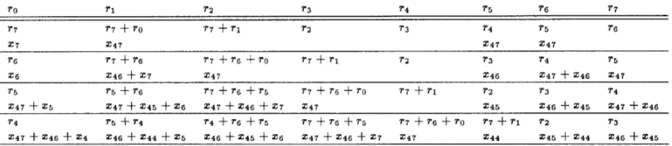
Based on the proposed translation method men- tioned above, the next state of the octet-parallel HEC generator is shown in Table 2. An observation on Ta- - ble 2 reveals that the responses are in regular sequence if each row is regarded as a state of the HEC gener- ator. It is easily seen that each row is the very next sate of the above row. This can be verified by the fol- lowing equations. For the HEC generator, X = e l and e i + l = T e ; . From Eq. (4), we can obtain
3.2
Scrambler
for
SDH-Based UN1
The self synchronizing scrambler with generating polynomial z 4 3
+
1 lhas been identified for the SDH- based physical layer. The scrambler and descrambler are slightly different from each other and are shown in Fig. 4.Q k + n = q8 * T15e1
+
* . 41.
T8ei+
Z k.
T 7 e 1in which
[.Ip(,)
denotes the remainder of the division by the polynomial P ( z ) . At the next clock cycle, the Table 2: Next State of HEC Generator in Parallel.Stimulus Response Stimulus Response values R + ( z ) left in the register will be
xk+7 ~ 0 0 0 0 0 0 0 4 1 11 100000 2k+6 0 ~ 0 0 0 0 0 0 q 2 011 10000 zk+5 0 0 ~ 0 0 0 0 0 q3 00111000 Zk+4 00010000 q 4 00011100 00001000 q 5 00001110 zk+l 0 0 0 0 0 0 ~ 0 q7 11100011 " k + 3 zk+2 00000100 q6 00000 11 1 10010001 zk 00000001 q a
Table 1 is slightly different due to the feedback link between the 28th and the 29th D flip-flops.
3.4
Cell Delineation
Although based on the same polynomial xa
+
x 2+
z
+
1 theoretically, cell delineation is somewhat dif- ferent from HEC generation. Before performing the division, The LFSR computing the remainder shall re- set its register t o all Os. Then 40 bits of header are applied in serial and the remainder is left in the regis- ter. After that, the LFSR will be reset again in order to compute another remainder. Fig. 6 illustrates this situation§. On the other hand, cell delineation will be-
1 40 40'
Figure 6: Fragmental Cell Delineation - Serial. performed bit by bit as shown in Fig. 7 .
Clearly, only z B ( z )
+
C
is desired and Az4' should be discarded. Therefore,b .
B ( z )+
Cl,(,)=
R+(z)
+
[ A Z * ' ] ~ ( , )= R + ( z )
+
A(a6+
c5+
z). (8) From Eq. (8), we can obtain the continuous HEC checker (bit by bit) shown in Fig. 8.Figure 8: Continuous HEC Checker.
For completeness and later use, consider the con- tinuous HEC checker in a backward way. Suppose that
The remainder of B(x) can be calculated using the formula
[ B ( Z ) l P ( , ) = 2 - l
[ R ( 4
+
Cl,
where z-l denotes the reverse operation of LFSR. For example, the reverse operation of the original HEC generator is shown in Fig. 9.
I I
Figure 9: Reversed HEC Generator. Figure 7: Continuous Cell Delineation - Serial.
Obviously, the original HEC generator should be modified so as to fit our need. Let P ( z ) = z ~ + z ~ + z + ~ and A , B ( z ) , C as shown in Fig. 7. Assume that the remainder of 40 bits of d a t a after the initialization is
R ( z ) , i.e.,
§The shaded box is the time slot with reset.
In the previous clock cycle, the remainder left in the register was
+
B ( 4 l p(,)2-l [ R ( z )
+
C]+ [AZ'~]
p(,)-
-
= z-l
[ R ( z )
+
C]
+
A ( z 5+
z4
+
1). (9) The continuous HEC generator/checker shown in Fig. 8 is in serial mode and it is desired to convert itinto an octet-parallel
HEC
generator/checker. While the translation method depicted in the previous sec- tion can be applied t o it directly, we describe another method which achieves the the same goal with reduced complexity and shorter delays instead.First, convert the original HEC generator in bit- serial mode into a n octet-parallel one depicted in
I
I I
R (4
Figure 12: Full Cell Delineation - Parallel.
By Eq. (9), three other remainders are obtained and listed in Table 4. It is seen that the number of Sec. 3.3. After translation, the HEC generator will
be operated in parallel as shown if Fig. 10. Remember
Figure 10: Fragmental Cell Delineation
-
Parallel. that cell delineation will be performed bit by bit. The above octet-parallel HEC generator should be further modified as shown in Fig. 11 for the first step. BelowFigure 11: Continuous Cell Delineation - Parallel. is a list of necessary equations to support continuous cell delineation in parallel depicted in Fig. 11. Suppose that
variables increases rapidly downward both in Table 3 and 4. The increase in the number of variables means more fan-ins and fan-outs in hardware, which should be avoided in implementation. That’s the reason why we use the forward and the backward method simulta- neously t o reduce the complexity of the hardware and t o achieve better performance.
4
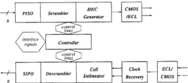
Implementation
The parallel architecture of the transceiver chip for the ATM cell-based
UN1 is shown in Fig. 13. The
operations of the scrambler/descrambler, HEC genera- tor, and cell delineator are all explained in the previous section. P I S 0 (Parallel In Serial Out) and S I P 0 (Se- rial In Parallel Out) perform the serial-parallel con- versions. The clock recovery circuit [lo] retrieves the correct clock signal from the bit-stream of data. The ECL/CMOS and CMOS/ECL pads [ll] perform CMOS/pseudo-ECL voltage level conversions, which are necessary in order to satisfy the high-speed require- ment. Table 5 summarizes the features of our parallel ACUNI chip.[A(z) * x3’
+
B ( z ) I P ( , )
= R ( z ) .
At the next clock cycle (in parallel), the values
R+(z)
left in the register will be
Generator Scrambler
[ A ( z ) * z 4 O - t z 8 * B ( a ) + C ( ~ ) ] p ( , ) .
Thus, we can obtain the remainder of
x8
-
B ( z )
+
C(z) Clockfrom
[.8
-
wz)
+
C ( ~ C > I
F,(,)=
R+
+
[ A ( ~ )-
z401.
Figure 13: Parallel Architecture of ACUNI.There is still seven remainders left blank between
the octet boundary. In order to carry it out, more
5
Conclusions
computations are necessary. In Fig. 12, assume that
T ( Z ) and R ( x ) are the remainders of the correspond-
ing data stream, respectively.
It
is desired that the seven remainders between the octet boundary should be expressed in terms of ~ ( z ) and R ( x ) together with( 2 4 7 , 2 4 6 , . *
,
2 4 0 , 2 7 , 2 6 ,-
e,
ZO}. From Eq. (8), fourof the remainders are obtained and listed in Table 3.
We have proposed a parallel architecture to ac- complish the operations stated in the ITU-T Recom- mendation 1.432. The principles of each function are explained and parallelized by translation method. Ac- cording to the experimental results, we know that par- allel architecture is really effective and reduces the
Table 3: Full Cell Delineation - Forward Method.
Table 4: Full Cell Delineation - Backward Method.
Ro RI R2 R3 R4 R5 R6 R7
RI
+
Ro R2+
Ro
R3 R4 R5 R6 R7 Ro1 4 0
+
0 0 1 0 1 4 0 1 4 0 1 0RI
+
Rz R3+
RI+
Ro R4 R5 R6 R7 Ro RI+
Ro[5] ITU-T Recommendation G.709, “Synchronous Table 5: Specifications and Features of Parallel ACU-
NI Chip. Multiplexing Structure,” Blue Book, 1989.
IC Process 0.8 pm SPDM CMOS Data Rate 155.52 Mbps (STM-1) Chip area 4331pm x 4277pm Transistor count 13317 Package PGA Pin count 68 Operation frequency 190 MHz
operating frequency significantly, with the hardware overhead.
References
R. Hiindel and M. N. Huber, Integrated Broad- band Networks - A n Introduction to ATM- Based Networks, Addison-Wesley, 1991.
ITU-T Recommendation 1.432, “B-ISDN User- Network Interface - Physical Layer Specifica- tion,” 1991.
ITU-T Recommendation G.707, “Synchronous Digital Hierarchy Bit Rates,” Blue Book, 1989. ITU-T Recommendation G.708, “Network Node Interface for the Synchronous Digital Hierarchy,”
Blue Book, 1989.
[6] Ing-Yi Chen, Chin-Chou Chen, Wen-Jay Lin and Sy-Yen Kuo, “ACUNI: A 155.52Mbit/s Transceiver Chip for ATM Cell-Based User- Network Interface,” Proc. of the Fifth VLSI De-
s ig n/CA D S y mp o s ium, 1 9 9 4.
[7] S. W. Golomb, Shift Register Sequences, rev. ed., Aegean Park Press, Laguna Hills, Californa, 1982. [8] W. W. Peterson and E. J . Weldon, Jr., Error- Correcting Codes, 2nd ed. MIT Press, Cambridge, Massachusset ts, 1972.
[9] Seok Chang Kim, Byeong Gi Lee, “Synchroniza- tion of Shift Register Generators in Distributed Sample Scramblers,” IEEE Transactions o n Com- munications, Vol. 42, pp. 1400-1408, 1994. [lo] Banu, M., A. E. Dunlop, “Clock Recovery Cir-
cuits with Instantaneous Locking,” Electronics Letters, Vo1.28, pp. 2127-2130, Nov, 1992. [ll] M. S. J. Steyaert, W. Bijker, P. Vorenkamp and
J . Sevenhans, “ECL-CMOS and CMOS-ECL In- terface in 1.2pm CMOS for 150MHz Digital E- CL Data Transmission Systems,’’ IEEE Journal
of Solid-state Circuits, Vol 26, pp. 18-23, Jan- uary, 1991.