雙異質結構光子晶體波導共振腔模態分析
66
0
0
全文
(2) 雙異質結構光子晶體波導共振腔模態分 析. 研 究 生 : 陳 佳 禾 指導教授 : 李柏璁 教授. 國立交通大學光電工程學系光電工程研究所碩士班. 摘要 隨著半導體製程技術的進步,光子晶體元件變的越來越小. 許多功能性的元件 可以整合在單一晶片上,且訊號可以在光子晶體內部傳遞而不會有太大的損失. 傳統上, 訊號會由光子晶體波導的側邊輸入, 這樣的輸入信號方式對於環境的振 動是相當敏感的. 只要一點微小的振動就能影響很大的光學損失.. 在這篇論文中,我們嘗試改變不同的輸入信號方式. 光會由垂直的被導入共振 腔內, 而我們有興趣的信號會被萃取出來且在波導內傳遞. 為此概念,我們設計 了一個雙異質結構光子晶體波導共振腔.我們使用三維的有限時域差分法來分析 共震模態及每個模態的品質因子. 元件已經成功的製作出來. 基本的平面及垂直 放射特性已經被得到.這種元件可以當作光積體電路中光萃取元件,且具對震動具 有較好的容忍度.. Ⅰ.
(3) Modal analysis of double hetero-structure photonic crystal waveguide-resonator. Student : Jia-Ho Chen Advisor : Prof. Po-Tsung Lee. National Chiao Tung University Department of Photonic & Institute of Electro-Optical Engineering. Abstract The sizes of photonic crystal devices become smaller with the advancement of semiconductor fabrication technology. Many functional devices can be integrated on the single chip. Signals can propagate in the photonic crystal with low optical loss. Traditionally, the signal will be side-pumped into the input waveguide, the insertion loss is sensitive to the vibration. It is easy to cause large optical loss with little vibration. In this thesis, we try to change the pumping direction. Light will be vertically pumped into the cavity and the signal of interest will be extracted and propagates in the waveguide. For this idea, we design and fabricated the double hetero-structure photonic crystal waveguide-resonator. Three dimensional finite difference time domain method are used to analyze each resonance modes and the quality factor of them. Devices have been successfully fabricated. The basically in-plane and vertical emission have been obtained. This device can be served as light extraction device in optical integrated circuit and better tolerance of vibration.. Ⅱ.
(4) Acknowledgements 終於~走到了這一步,長達 16 年的學生生涯就要在這裡畫上了句點。我想我能 完成所有的學業,首先就是要感謝我的父母,尤其是我的父親,為了子女的教育,不 辭勞苦 , 只為了讓我們將來能過好的生活 , 不要像他一樣做苦工。同時也要感 謝我的母親 , 因為整個家裡大大小小的事都是他來整理 , 是一個標準的好媽 媽。 碩班兩年 , 還是得先感謝我的指導教授李柏璁老師 , 讓我在研究上有很自 由的發揮空間 , 同時给與適當建議 , 再來感謝博班學長盧贊文 , 幫我解決量 測問題 , 同時幫我解答許多的研究上問題 , 還有時常請我們吃東西。還有學長 張資岳 , 時常分享國外的顯示技術 , 讓我多增加了不少知識。再來 , 我的同學 們 , 阿德時常找我去游泳 , 讓我游泳技術精進了不少 , 希望阿德趕快交女朋 友 , 不要在娘了啦 ! 同時時常拜託我幫他寫 E-Beam , 讓我製程技術也同時精 進 。 仲銓 , 嘉銘 , 思元,當我在實驗上有問題 , 也能給予我許多意見 。 除此 之外 , 研究之餘 , 大家一起玩樂 , 讓我碩班 2 年增添許多美好回憶 。. 再來我要感謝以前畢業的學長 , 蘇國輝 , 時常找我們去看電影 , 還有陳書 志 , 陳鴻祺 , 將他們所學都交給了我 , 雖然我沒能將其發揚光大(汗)~最後要 感謝新進的學弟妹們, 蔡宜育 , 施均融 , 王明璽 , 宋和璁,有你們本實驗室多 了不小歡笑還有趣事 , 還有本實驗室有史以來第一個學妹~林孟穎 , 讓我們時 常有餅乾可以吃 , 有八卦可聽 , 其實學妹很正的 , 又多才多藝 , 喜歡的趕快 追吧! 哈~學弟妹們都有唸博士的資質 , 實驗室靠你們了,加油!!. 2007/7/6 于新竹 國立交通大學. Ⅲ.
(5) Content Abstract (in Chinese) ---------------------------------------------------------Ⅰ Abstract (in English) ----------------------------------------------------------Ⅱ Acknowledgements-------------------------------------------------------------Ⅲ Content---------------------------------------------------------------------------Ⅳ List of tables---------------------------------------------------------------------Ⅴ List of figures--------------------------------------------------------------------Ⅵ Chapter 1. Introduction 1.1 Introduction of photonic crystals-----------------------1 1.2 Photonic crystal Hetero-structure----------------------5 1.3 The applications of photonic crystal hetero-structure-------------------------------------------8 1.4 Motivation and overview--------------------------------11. Chapter 2. Device design and simulation results 2.1 The numerical methods used in photonic crystal simulation------------------------------------------------------12 2.1.1 Maxwell equation in non-uniform dielectric medium----------------------------------------12 2.1.2 Plane Wave Expansion Method-------------14 2.1.3 Finite-Difference Time-Domain Method--16 2.2 The cavity design using selective mirror--------------19 2.3 The cavity mode analysis -------------------------------23 2.3.1 Identify each cavity mode and mode profiles.
(6) ---------------------------------------------------23 2.4 Quality factor analysis------------------------------------25 2.4.1 The calculation method of Quality factor and accuracy test-------------------------------------25 2.4.2 Quality factor for each mode existed in the double hetero-structure cavity----------------32 2.5 Conclusion ------------------------------------------------35 Chapter 3. Fabrication process for double Hetero-structure edge emitting laser . 3.1 Fabrication processes for membrane structure--------36 3.2 Cad design and SEM picture----------------------------40 3.3 Conclusion ------------------------------------------------43. Chapter 4. Measurement results 4.1 Measurement system-------------------------------------44 4.2 Identify the lasing modes--------------------------------46 4.3 The lasing characteristic of mode D in both vertical and in-plane direction-----------------------------------48 4.4 Conclusion-------------------------------------------------51. Chapter 5. Conclusion------------------------------------------------------52. References------------------------------------------------------------------------53. Ⅳ.
(7) List of tables 1. Table 2.1 Comparison of quality factor with different grid size---------------------31 2. Table 2.2 Simulation parameters---------------------------------------------------------33 3. Table 3.1 ICP/RIE recipes----------------------------------------------------------------37. 4. Table 3.2 Fabrication tolerance of each dry and wet etching step------------------40 5. Table 3.3 The comparison between target and fabrication parameter of our device---------------------------------------------------------------------------------------40. Ⅴ.
(8) List of figures Chapter 1 1. Fig.1-1 An example of photonic crystal, different colors mean different dielectric constants. (a) 1-D (b) 2-D (c)3-D---------------------------------------------------------2. 2. Fig.1-2 The band diagram of triangular photonic crystal with air holes defined on the slab. (a)without introducing defects and(b)with a point defect.------------------4 3. Fig. 1-3 The band structure of photonic crystal with different lattice constants. Green dotted line : a=465 nm r/a=0.0.296 Red dotted line: a=460 nm ,r/a=0.3. The configuration of photonic crystal waveguide is shown on the bottom of the figure.-----------------------------------------------------------------------------------------6 4. Fig.1-4 The transmission spectra for of two photonic crystals with different lattice constants. (Ι) a = 465 nm(line with open circle) ,(Π) a = 460 nm( line with open square) --------------------------------------------------------------------------------------------7. 5. Fig.1-5(a) The schematic illustration of the photonic crystal hetero-structure cavity (b) the schematic band diagram of the photonic crystal hetero-structure cavity. Dash line represents the frequency of resonance mode.----------------------8 6. Fig1-6 (a) Schematic of the multi-channel add/drop filter (b) The drop spectra of four port channel add/drop filter.(Adopted from the reference 9) -------------------9 7. Fig.1-7 A demo of optical integrated circuit. The original input signal is pumped into the waveguide-resonator vertically and be extracted into the optical circuit. The processed signals can also be extracted out of the optical circuit vertically and become the input signal of another optical circuit------------------------------------11. Chapter 2 1. Fig.2-1(a) The TE band diagram of triangular lattice photonic crystal (b) The.
(9) supercell used in the simulation.---------------------------------------------------------15 2. Fig. 2-2 The scheme of Yee cell----------------------------------------------------------17 3. Fig. 2-3 (a)The scheme of channel drop filter (b) The mode profile on the steady state (c)The transmission spectrum on the resonance frequency and(d) the reference transmission of single line defect waveguide-------------------------------20 4. Fig.2-4 (a) The structure of the device with cavity region and output waveguide separated by the dash line.. (b) The cavity region is formed by slightly shifting. the six air holes outward from the waveguide.-----------------------------------------21 5. Fig.2-5 (a) The TE band structure of the cavity region without and with shifting six air holes. Red dotted line : the defect modes without shifting any air holes. Blue dotted line : the defect modes with shifting the six air holes 30nm outward from the surrounding waveguide. Green dotted line : the defect modes with shifting the six air holes 50nm outward from the surrounding waveguide. (b) The supercell used in the simulation----------------------------------------------------------22 6. Fig.2.6 The plot of resonance frequency versus r/a ratio for each mode. The gray shadow mark the region of photonic band gap. There are seven cavity modes existed in this cavity due to the effect of mode gap confinement.-------------------23 7. Fig. 2-7 (a) the contour map of index profile of whole device. The contour map of refractive index which grid size is equal to (b) Period/24 and (c) Period/64.-----27 8. Fig.2-8 The contour maps of transverse index profile on the half X-Y plane where grid size is equal to (a)Period/24 and (b) Period/128.--------------------------------28 9. Fig. 2-9 The quality-factor simulation setup and the setting of time monitor.----29 10. Fig.2-10 (a) The energy density detected by time monitor1, 2, and3 versus time duration (b) The fitted data of time monitor 1 with first order exponential decay.----------------------------------------------------------------------------------------29 11. Fig.2-11. The transverse index profile while grid size(Y) is equal to 44nm and.
(10) simulation domain (Y) is set to 308nm. The graded-index layer is disappear.----32 12. Fig.2-12 The quality factor for each resonant mode.----------------------------------33. Chapter 3 1. Fig.3-1 The epitaxial structure of InGaAsP/InP MQWs wafer.----------------------36 2. Fig.3-2 A flow chart of fabrication processes for membrane structure.-------------39 3. Fig.3-3 The CAD layout of our device.-------------------------------------------------41 4. Fig. 3-4 (a)(b) The SEM pictures of the devices with successful undercut The (c) Top view and (d) side-view SEM pictures after cutting. -----------------------------42. Chapter 4 1. Fig.4-1 (a) The configuration of micro PL measurement system.(b) (c) The configurations of measurement setup---------------------------------------------------45 2. Fig.4-2 Identify the lasing modes by the simulation data. There are three possible lasing modes, mode B, mode C, and mode D------------------------------------------46 3. Fig.4-3 The vertical lasing spectrum above threshold of device 1 in (a) linear and (b) dB scale.(c)The L-L curve and (d)The SEM picture of device 1----------------48 4. Fig.4-4 The in-plane lasing spectrum above threshold of device 1 in (a) linear (b) dB scale.-------------------------------------------------------------------------------------49 5. Fig.4-5 The vertical lasing spectrum above threshold of device 2 in(a) linear and(b) dB scale.(c)The L-L curve and (d)The SEM picture of device 2--------------------50 6. Fig.4-6 The in-plane lasing spectrum above threshold of device 2 in (a) linear and (b) dB scale.---------------------------------------------------------------------------------50. Ⅵ.
(11)
(12) Chapter 1 Introduction 1.1 Introduction of photonic crystals Photonic crystal, which possesses the ability to control the flow of light , was firstly proposed by Yablonovitch in 1987[1] . At the beginning, the concept of photonic crystal was not widely accepted by the scientific researchers due to the issues of realization of three dimensional photonic crystal which possessed complete photonic band gap . In 1989, Yablonovitch and Gmitter have tried to demonstrate that complete three dimensional photonic band gap existed experimentally. Although the experiment was finally failed, many scientific researchers have started to pay more attention on this new research area. More and more research results have been reported in resent years. Photonic crystal is composed of different materials whose index are periodically arranged on space[2]. The simplest artificial photonic crystal is one dimensional multilayer structure as illustrated in Fig.1-1(a), which is the same with some kinds of optical thin films. This kind of structure can be coated on the lens or mirrors to enhance the transmission or refection of light in specific frequency. The more complicated structures of photonic crystal illustrated in Fig. 1-1 (b) and (c) are that the dielectric constants are periodically arranged in two and three dimensions. Various applications of those complicated structures in optoelectronic such as filter, quantum well laser, optical waveguide and so on, are designed and proposed.. 1.
(13) Fig.1-1 An example of photonic crystal, different colors mean different dielectric constants. (a) 1-D, (b) 2-D , and(c) 3-D. In previous section, we talk about that 1-D photonic crystal can enhance the transmission or reflection of light in specific frequency range. Generally speaking, when light meets photonic crystal, it will be totally reflected or partially pass through the photonic crystal. This phenomenon in photonic crystal is so called photonic band gap. The concept of photonic band gap can be regarded as optical analog of electrical band gap existed in semiconductor. Atoms in the solid crystals produce the periodic potential so that electrons are confined in the periodic potential well. The energy of electrons is quantized and the dispersion relation is banding alike. In fact, each band represents a series of discrete energy levels. The gap between each band is called “forbidden band”, which means that there are no allowed energy levels in this region. Similarly, the dispersion relation of photonic crystal is also banding alike and no photons are allowed to exist in the forbidden bands. This is the reason of light in certain frequency range within the forbidden band meets the photonic crystal will be reflected. Because the photons can not be propagate in photonic crystal.. 2.
(14) However, in the view of application, we hope that light can exist in the photonic crystal and be controlled. This goal can be achieved by introducing artificial defects. Take the 2-D photonic crystal shown in Fig.1-2 for example, the photonic crystal patterns are defined on the slab. Before introducing the point defect, the band structure with clear photonic band gap (PBG) is shown in Fig. 1-2(a). When removing one air hole for forming the defect and band structure is shown in Fig. 1-2(b), we can discover that a defect mode appears in the original PBG.. This defect mode can be localized in this defect by PBG effect in in-plane direction and total internal reflection (TIR) in vertical direction. This is a typical photonic crystal micro cavity with high Quality factor and a small mode volume. Recently, Noda et al has proposed the high performance photonic crystal cavity with its Quality factor being close to 100,000[3] which can be applied to design high efficiency channel drop filter [4-9]. If we introduce a line defect, light can be guided within the photonic crystal. Photonic crystal waveguide is attractive in the optical communication due to its optical loss of 1dB per millimeter [10] and 900 waveguide bend with the optical loss is lower than traditional optical fiber [11].. In recent years, many researchers have started to integrate the photonic crystal cavity and waveguide to realize the functional devices, such as optical bistable switch [12], slow light components [13], channel drop filters, and so on.. 3.
(15) Fig.1-2 The band diagram of triangular photonic crystal with air holes defined on the slab. (a)without introducing defects and(b)with a point defect.. In order to improve efficiency of these devices, cavity design has become an important issue. Many researchers fine tune the air hole shape and position near the cavity to achieve this goal. But sometimes this method will result in tough fabrication issues. Therefore, some researchers bring up the ideal that using hetero-structure to optimize the modal in-plane confinement. By using hetero-structure, we can avoid tough fabrication issues, and cavity quality factor can be greatly increased [14]. In next section, we will discuss how the hetero-structure can be formed in photonic crystal.. 4.
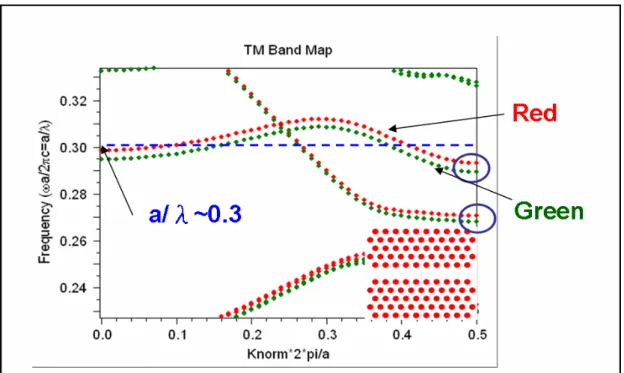
(16) 1.2 Photonic crystal hetero-structure Over the past decades, hetero-structure has been widely used in semiconductor. In semiconductor, hetero-structure can be formed by using different band-gap materials and strains. However, molecular beam epitaxy costs lots of money and lattice constant mismatch problem will restrain the usage of materials. In photonic crystals, the formation of hetero-structure is more elasticity.. Generally, the hetero-structure can be created by simply tuning the size of air holes in different region of photonic crystal region. However, it is difficult to control the size of air holes due to proximity effect and unstable electron beam dosage in the electron beam lithography process. The better way is to vary the lattice constant of photonic crystal. The lattice constant shift will result in the frequency shift of each band. As shown in Fig.1-3, the red and green dotted lines represent the defect modes of photonic crystal waveguide with different lattice constants. The circles mark the frequency difference between red and green dotted lines. Photons will be reflected in the hetero-junction due to this slightly frequency difference. This effect is called as “mode gap confinement”and can be used to design a prefect mirrors.. The hetero-structure interface plays an important role, acting as a nearly perfect but frequency selective mirror for photons. Reflectivity of this mirror can be nearly up to 100% when the frequency of input photons is within the mode gap and can be relative low when frequency is outside the mode gap. The transmission spectra for two photonic crystals with different lattice constants are shown in Fig.1-4.. 5.
(17) Line with open circle represents the transmission of the photonic crystal with lattice constant set as 465nm, and the line with open square represents the transmission of the photonic crystal with lattice constant set as 460nm. We can clearly see the transmission spectra will shift to high normalized frequency region with shorter lattice constant. If we see the specific frequency, for example a/λ=0.3 which is shown in Fig.1-4, light propagate in the photonic crystal with long lattice constant will be strongly reflected when enter the photonic crystal with short lattice constant.. The applications of selective mirrors are attractive in many functional devices. Next section we will discuss these applications.. Fig. 1-3 The band structure of photonic crystal with different lattice constants. Green dotted line : a=465 nm r/a=0.296. Red dotted line: a=460 nm ,r/a=0.3. The configuration of photonic crystal waveguide is shown on the bottom of the figure.. 6.
(18) (a/λ) Fig.1-4 The transmission spectra for of two photonic crystals with different lattice constants. (Ι) a = 465nm(line with open circle) (Π) a = 460nm( line with open square). 7.
(19) 1.3 The application of hetero-structure So far, we talk about that hetero-structure can be served as perfect but frequency selective mirrors. The applications of selective mirrors are important in many functional devices design.. One typical example is photonic crystal hetero-structure cavity [17] which is shown in the Fig.1-5(a). In the central region, light with certain frequency within the pass band will encounter the stop band of the surrounding photonic crystal. Electromagnetic wave will be confined in the central region and resonant. The schematic band diagram is shown in the Fig.1-5(b). The frequency of resonance mode which drops to the mode-gap of surrounding photonic crystal is represented as dash line.. (a). (b). Fig.1-5(a) The schematic illustration of the photonic crystal hetero-structure cavity (b) the schematic band diagram of the photonic crystal hetero-structure cavity. Dash line represents the frequency of resonance mode.. Another example is multi-channel drop filter. The multi-channel drop filter can extract the signals with specific wavelengths and is useful in the WDM system.. The. hetero-structure is a key component in realizing the function of multi-wavelength due 8.
(20) to its frequency selective property. Noda et al proposed a four port channel drop filter in 2005 [9] as shown in the Fig.1-6(a). The drop efficiency is approach to 100% for each wavelength and the wavelength integral is about 20nm. The drop spectra is shown in the Fig.1-6(b).. (a). (b) Fig1-6 (a) Schematic of the multi-channel add/drop filter (b) The drop spectra of four port channel add/drop filter. (Adopted from the reference 9). 9.
(21) Selective mirrors can also be used to enhance the quality factor of cavity. By using double hetero-structure, we can match the envelope function of electric field with the envelope function of Gaussian Beam. The energy loss due to envelope function distortion can be further decreased. The reported extremely high quality factor of 600000 has been achieved experimentally by Noda in 2005 [14], which is the highest value in the world in recent years.. 10.
(22) 1.4 The Motivation and Overview In photonic-crystal research area, the final goal is to realize ” optical integrated circuits”. The signals can be processed in single chip and be extracted to another one. However, it is difficult to import signals into the optical circuit from the horizontal cross-section of the input waveguide. On the contrary, it is easy to pump signal into a cavity vertically. As a result, it is possible to import signal vertically into a optical circuit. However, there is only little literature are published on this issure.. In this paper, we propose a device named “double hetero-structure waveguide-resonator”. The double hetero-junctions are employed to create in-plane confinement of this waveguide-resonator. We analyze the resonance modes of this resonator numerically and experimentally. We hope this device can successfully extract signal from vertical into in-plane direction. Fig. 1-8 illustrates this idea graphically.. Original Input signal. The input signal of another optical circuit Fig.1-7 A demo of optical integrated circuit. The original input signal is pumped into the waveguide-resonator vertically and extracted into the optical circuit. The processed signals can also be extracted out of the optical circuit vertically and become the input signal of another optical circuit. 11.
(23) Chapter 2 Device design and Simulation results 2.1 The numerical methods used in photonic crystal simulation In this section, we begin with the Maxwell equations, which are the rules of light propagating in the free space and media. Then, we will introduce the two major numerical methods used in the photonic crystal : (1) Plane wave expansion (PWE)(2)Finite difference time domain(FDTD) method.. 2.1.1 Maxwell equation in non-uniform dielectric medium. Light propagating in the space will obey the Maxwell equation listed below owing to its wave nature: ∇i( D) = 4πρ ∇i B = 0 1 ∂B ∇× E = − c ∂t 1 ∂D 4π J ...2.1 ∇× H = + c ∂t c. Where E and H donate electric and magnetic filed, B and D donate magnetic flux density and displacement field, and c is light speed in free space. The definitions of D and H are as follow : D = ε (r ) E + P B H= −M μ (r ). P: polarization vector(C/m 2 ) M: Magnetization vector(A/m 2 )...2.2. In general case, ε and μ are the function of space and cannot be remove outside of the ▽ operator. Now if we only consider the dielectric and nonmagnetic medium , then μis constant and is equal to 4π×10-7(H/m) and M is equal to 0. The general form of D. 12.
(24) field is more complex because the polarization vector is not only the function of space but also the function of electric field. The formula of D is : ~. ~. ~. ~. P (t ) = χ (1) E (t )+ χ (2) E 2 (t ) + χ (3) E 3 (t ) + ... Di = ∑ ε ij E j + ∑ k χ ijk E j Ek + O( E 3 ) j. j. ~. ~. where P (t ) and E (t ) are scalar field...2.3. However, we usually assume the intensity of excitation light is smaller enough so that the nonlinearity can be ignored. If we further assume the material is isotropic and homogeneous in all space, the D filed can be simply reduced to the form: D(r ) = ε 0ε r (r ) E (r )...2.4 Next, we use equation (2.4) to replace the electric field in equation (2.1) and do some curl operation and substitution, we can get the wave equation in source free region: Ω E E (r ) =. 1 ω2 ∇ × {∇ × E (r )} = 2 E (r )...2.5 ε (r ) c 1 ω2 ∇ × H (r )} = 2 H (r )...2.6 ε (r ) c. Ω H H (r ) = ∇ × {. Solving equation (2.5) and (2.6) are the eigenvalue problems. Both Ω E and Ω H are Hermitian operators, so the eigenvalue. ω2 c2. and eigenvectors E (r ) and H (r ) are. real number and can be solved by numerical method.. 13.
(25) 2.1.2 Plane Wave Expansion Method. Plane wave expansion is a powerful method for the band-diagram calculation of photonic crystal. This method is similar to the way to deal with the behavior of an electron (Kronig-Penney Model) in the periodic potential in solid-state physics. The periodic potential can be expressed as a complex fourier series(2.7) by using the reciprocal lattice vector ( G ). Similarly, the wave function of electron in periodic potential can also be expanded by the plane waves which are belong to the complete set of schrodinger equation (2.9). Periodic potential : U (r ) = ∑ U G eiG i R ...2.7 G. Periodic dielectric distribution : ε (r ) = ∑ ε G eiG i R ...2.8 G. For the same reasons, periodic dielectric distribution can also be expanded by reciprocal lattice vector(2.8) and the wave function of photon in periodic dielectric distribution can also be expanded by the plane waves which are belong to the complete set of wave equation(2.10). Wave function of Electron : ϕk (r ) = ∑ C (k − G )ei ( k −G ) i R ...2.9 G. Wave function of Photon: ψ k (r ) = ∑ M (k − G )ei ( k −G ) i R ...2.10 G. Finally, we substitute the equation (2.8) and (2.10) into (2.5), we will get new wave equation :. (k + G ) • (k + G′) × EG′ = −ω 2 ∑ ε G ,G′ EG′ ...2.11 G′. This equation can be expressed as a matrix form and the dispersion relation can be solved. The wavevector k is arbitrary, but can be replaced by k in the first Brillouin zone which is due to the translational symmetry inhered in photonic crystal. Therefore, 14.
(26) we can limit our calculation in the first Brillouin zone. The ε G ,G′ is the fourier coefficient of ε (r ) and ε −1 (r ) ,which is concerning to G − G ′ . All band diagrams of photonic crystal in this paper are calculated by this method. At first, we should define a supercell which is similar to the unit cell in solid crystal. The supercell of this band diagram is shown in Fig.2-1(a). It should be kept in mind that the configuration of photonic crystal can always be expanded by the defined supercell. Fig. 2-1(b) is a typical TE band diagram for triangular lattice photonic crystal calculated by PWE. (a). (b). Fig.2-1(a) The TE band diagram of triangular lattice photonic crystal (b) The supercell used in the simulation.. 15.
(27) 2.1.3 Finite-Difference Time-Domain Method. Defect engineering is an important issue in designing the photonic crystal devices. However, PWE method is applicable in calculating band structure, but can not provide the time dependent behavior of light. As a result, the better way is to directly solve the Maxwell equation.. Maxwell equations are vector differential equations, but computers can only execute scalar add or subtract operations. Therefore, we should transform Maxwell equations into six scalar differential equations. FDTD Method is developed according to this ideal.. The six scalar differential equations for each field component of Faraday’s law and Ampere’s law are given by equation (2.12), where s and σ donate the magnetic loss and conductivity. ∂E y. ∂Ez ∂ = ( s + μ0 μr ) H x ∂z ∂y ∂t ∂Ez ∂Ex ∂ − = ( s + μ0 μ r ) H y ∂x ∂z ∂t ∂Ex ∂E y ∂ − = ( s + μ0 μ r ) H z ∂y ∂x ∂t ∂H z ∂H y ∂ − = (σ + ε 0ε r ) Ex ∂y ∂z ∂t ∂H x ∂H z ∂ − = (σ + ε 0ε r ) E y ∂z ∂x ∂t ∂H y ∂H x ∂ − = (σ + ε 0ε r ) Ez .......2.12 ∂x ∂y ∂t −. In general case, distribution of refractive index is not uniform and may be dependent on the positions. Hence, in order to describe the distribution of refractive index in detail, all space are divided into many ideal grids, each grid will be given one 16.
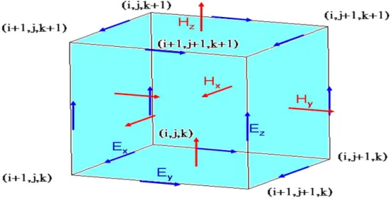
(28) refractive index which is the average index for each grid.. The widely used grid form adopted in the FDTD is Yee cell as shown in Fig.2-2. In Yee cell, the electric fields are arranged on the edges of the cubic, and the magnetic fields are centered on the facet, which is due to the electric fields updated are induced midway during each time step between successive magnetic fields, and conversely.. Fig. 2-2 The scheme of Yee cell. The index i, j, and k mark the positions of grid points in Cartesian coordinates. Therefore, the function of electric and magnetic field at the nth time step can be expressed as F (iΔx, j Δx, k Δx, nΔt ) = F n ( xi , x j , xk ) , where Δx is the increment of length and Δt is the increment of time step. The partial differential of six field components can be given as follow :. 17.
(29) ∂F n ( xi , x j , xk ) ∂xi ∂F ( xi , x j , xk ). =. n. ∂x j ∂F n ( xi , x j , xk ) ∂xk ∂F n ( xi , x j , xk ) ∂t. F n ( xi +1/ 2 , x j , xk ) − F n ( xi −1/ 2 , x j , xk ) Δx F ( xi , x j +1/ 2 , xk ) − F n ( xi , x j −1/ 2 , xk ) n. = = =. Δx F n ( xi , x j , xk +1/ 2 ) − F n ( xi , x j , xk −1/ 2 ) Δx F n +1/ 2 ( xi , x j , xk ) − F n −1/ 2 ( xi , x j , xk ) Δt. ...2.13. Furthermore, we substitute equation. (2.13) into equation. (2.12), and the six field components Exn +1/ 2 , E yn +1/ 2 , Ezn +1/ 2 , H xn +1/ 2 , H yn +1/ 2 , H zn +1/ 2 at the n+1/2 time step can be expressed with the field at the nth time step. The detail mathematical expression can be found in reference 16. The distribution of whole electromagnetic wave can finally be obtained. Although this method can provided highly accurate results, it costs lots of computational resources. Hence, powerful parallel computation such as cluster is needed.. 18.
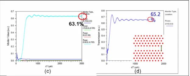
(30) 2.2 The cavity design using selective mirror Conversional photonic crystal micro-cavity uses the closed boundary which is formed by air holes. However, in order to achieve in-plane emission, the boundary of cavity should be open and directly engaged with output waveguide. Now, the problem is that whether the in-plane conferment of this kind of cavity is enough? We take an example to answer this question. The scheme of a simple channel drop filter is shown Fig2-3(a). We use the same way mentioned in reference [15] to tune the positions of six air holes near the edge of the L3 cavity in order to increase the quality factor of the cavity. Two 5-period selective mirrors by shifting the position of each hole 0.045 period to left side are added which is represented by open square in Fig2-3(a). Light will be imported in the port 1 and dropped at port 4. The transmission spectra on resonant frequency is shown in Fig.2-3(c). The drop efficiency is up to 96.8%(96.8%= 0.631 ÷ 0.652 × 100% ) when compared with the reference transmission of single line defect waveguide which is shown in Fig2-3(d). The mode profile on the steady state is shown in Fig2-3(b). We can clearly see that almost no light will pass through the selective mirror. From this example, we can see that the in-plane confinement of selective mirror is enough for specific frequency.. 19.
(31) Fig. 2-3 (a) The scheme of channel drop filter (b) The mode profile on the steady state (c) The transmission spectrum on the resonance frequency and (d) the reference transmission of single line defect waveguide.. As a result, our goal is to achieve in-plane emission, so in-plane confinement is still needed in order to let photons not only resonant in in-plane direction but also can be directly coupled into the output waveguide. Based on these two points, a promising approach is to employ the selective mirrors. Now, the scheme of the device is illustrated in Fig.2-4 (a). The output waveguide region is formed by taking three rows of air holes away. The cavity region is formed by slightly shifting the six air holes (red circles) outward from the waveguide, which is seen in the Fig.2-4(b).. The dash line stands for the hetero-junction formed by selective mirror. Someone may doubt that “Are there any selective mirrors?”. The answer is “yes”. This point can be explained by the band structure. The band structure of the cavity region without shifting and with shifting six air holes is shown in Fig.2-5. The red dotted line stands for the defect modes without shifting any air holes. The blue and green dotted line stands for the defect modes with shifting the six air holes 30nm and 50nm. 20.
(32) outward the surrounding waveguide. Clearly, the defect modes with shifting air holes drop into the modegap of original band structure. Conversely, the red dotted line is in the modegap of the blue and green ones.. (a). (b). Fig.2-4 (a) The structure of the device with cavity region and output waveguide separated by the dash line.. (b) The cavity region is formed by slightly shifting the. six air holes outward from the waveguide. As the result, if the light is pumped vertically into the central region between two hetero-junctions, it will be confined in the central region and resonant. The central region is a cavity. The lattice constant of the device is 480nm and r/a = 0.3, the band structure is calculated with PWE and effective index is 2.7 which is calculated with finite-element method.. 21.
(33) (a). (b). Fig.2-5 (a) The TE band structure of the cavity region without and with shifting six air holes. Red dotted line : the defect modes without shifting any air holes. Blue dotted line : the defect modes with shifting the six air holes 30nm outward from the surrounding waveguide. Green dotted line : the defect modes with shifting the six air holes 50nm outward from the surrounding waveguide. (b) The supercell used in the simulation.. 22.
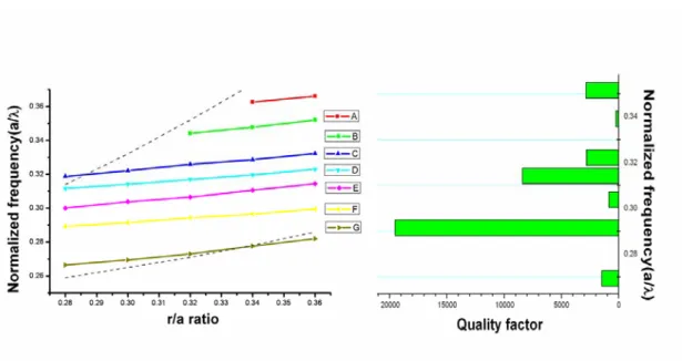
(34) 2.3 The cavity mode analysis In this section, I used the three-dimensional FDTD to calculate the resonant spectrum and the resonant mode profiles for each field component Ex, Ez, Hy.. 2.3.1 Identify each cavity mode and mode profiles In the beginning of this section, we firstly show the plot of resonance mode frequency versus r/a ratio which is shown in Fig.2-6. The gray shadow region is the band gap region. There are seven cavity modes existed in this cavity due to the effect of mode gap confinement.. Fig.2.6 The plot of resonance frequency versus r/a ratio for each mode. The gray shadow mark the region of photonic band gap. There are seven cavity modes existed in this cavity due to the effect of mode gap confinement.. 23.
(35) The mode profiles shown in the Fig.2-6 is the total electric field pattern, The mathematical expression of total electric field is given by equation (2.14) 2. 2. Etotal ( xi , z j ) = ( Ex ( xi , z j ) + Ez ( xi , z j ) ) For i,j = 0,1,2,3.... ...2.14. We load the data files of Ex and Ez which are produced by the Rsoft into Matlab, and note that the data should be converted into matrix form firstly. Secondly, we calculate the total electric field by using the equation (2.14), and then the field pattern of total electric field can be plotted.. 24.
(36) 2.4 The Quality factor analysis. 2.4.1 The calculation method of Quality factor and accuracy test. The quality factor is a target which is used to estimate the loss of a cavity. The definition of the quality factor of a cavity is given by equation (2.16) Q=. Total Energy stored in a cavity ...2.16 Energy loss per oscillation of a cavty. If the quality factor is large, it means that light can oscillate in the cavity for a long period before radiation into air. Conversely, small quality factor means that light can easily radiate into air. In other word, this cavity has poor light-confinement.. To calculate the quality factor, the most common way is to estimate the full width half maximum(FHWH) of the resonant peak. However, the resolution of the grid step will affect the accuracy of the calculated result, especially for high-Q cavity. Therefore, another method to calculate quality factor is adopted in this paper. We start from the energy decay equation which is given by equation (2.17), dE 1 = − E...2.17 τp dt. the solution of this equation is given by equation (2.18), then we can clearly see that E (t ) = E (0) exp(−. 1. τp. t )...2.18. the time-dependent behavior of energy stored in the cavity is exponential decay. As a result, we can estimate the quality by finding out the time constant when energy is decay to1/e. The final expression of quality factor is given by (2.19) Q=. ωE − dE. = ωτ p = 2π f τ p ...2.19. dt. Here, we calculate the energy decay verse time with the light tool developed by R-soft,. 25.
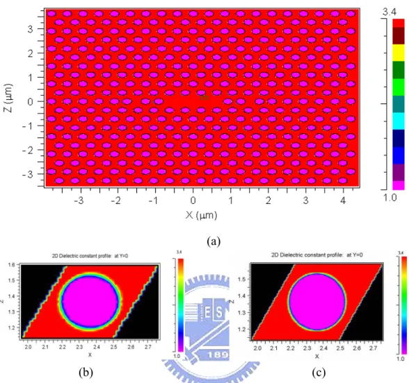
(37) and then we fit the energy decay curve to find out the time constant. At last, we calculated the quality factor by equation (2.19).. At first, we have to make sure that our simulated result is correct before calculating our own structure. To this end, we take L3 cavity [3] as a test in order to verify the accuracy of the simulation result. All the parameters including lattice constant, r/a ratio, refractive index, and so on will be set as the same with those mentioned in reference 3.. The accuracy of the calculated quality factor is directly influenced by the grid size, especially in the vertical direction. In general, the smaller the grid size is, the better the result we obtain. However, smaller grid size will enormously increase the simulation time, and costs lots of computational resource. In fact, we don’t know how small the grid size should be in order to obtain the correct result. As a result, we try to get the most approximately results as possible as we can in this paper.. The refractive index profiles of X-Z plane is shown in the Fig. 2-7. From the Fig2-10(b) and (c), we observe that the contour of air hole with grid size equal to Period/24 don’t have much difference when compared with grid size equal to Period/64. As a result, we suppose that this grid size is enough to resolve the shape of air holes in the x and z direction. So the grid size in the x and z direction is set to this value in this simulation.. 26.
(38) (a). (b). (c). Fig. 2-7 (a) the contour map of index profile of whole device. The contour map of refractive index which grid size is equal to (b) Period/24 and (c) Period/64.. The key point is the interface between air and slab which is concerned with the grid size in the y direction. The contour maps of transverse index profile on the half X-Y plane with different grid size are shown in the Fig. 2.8. We can obviously observe that the graded-index layer between air and slab layer is gradually disappear with the finer grid size. For calculation of quality factor, the grid size in y direction should be as smaller as possible, but it is unnecessary for the calculation of resonant spectrum and mode profile.. 27.
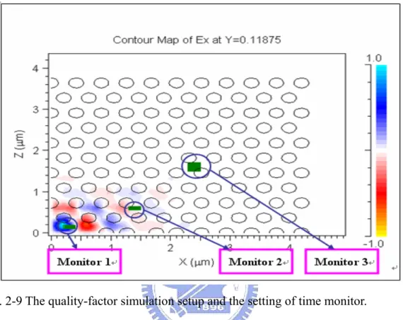
(39) (a). (b). Fig.2-8 The contour maps of transverse index profile on the half X-Y plane where grid size is equal to (a)Period/24 and (b) Period/128.. Before calculation, some details should be noted in the simulation are listed as follow : 1. The size of energy monitor should be smaller than that of a cavity in order to prevent including energy loss outside the cavity region. The detected energy density is a time-averaged value which is averaged from all the values received by the monitor. 2. One or more energy monitors should be added outside of the cavity to make sure the energy loss from the in-plane direction is about 0 (theoretically, we assume the in-plane Q is infinite for a closed-boundary cavity ). All suggestions mentioned above are illustrated in Fig.2-9. Time monitor 1 detects the energy density inside the cavity. Time monitors 2 and 3 detect the energy loss outside the cavity. The energy density detected by time monitor1, 2, and 3 versus time are shown in Fig.2-10(a) . We can see that energy decays exponentially for time monitor 1 and 2. The energy detected by the monitor 3 is approximate to 0 so that we 28.
(40) can make sure no energy will leaky out of the photonic crystal pattern. And then fit the data of time monitor 1 with first order exponential decay. The result is shown in Fig.2-10(b).. Fig. 2-9 The quality-factor simulation setup and the setting of time monitor.. (a). 29.
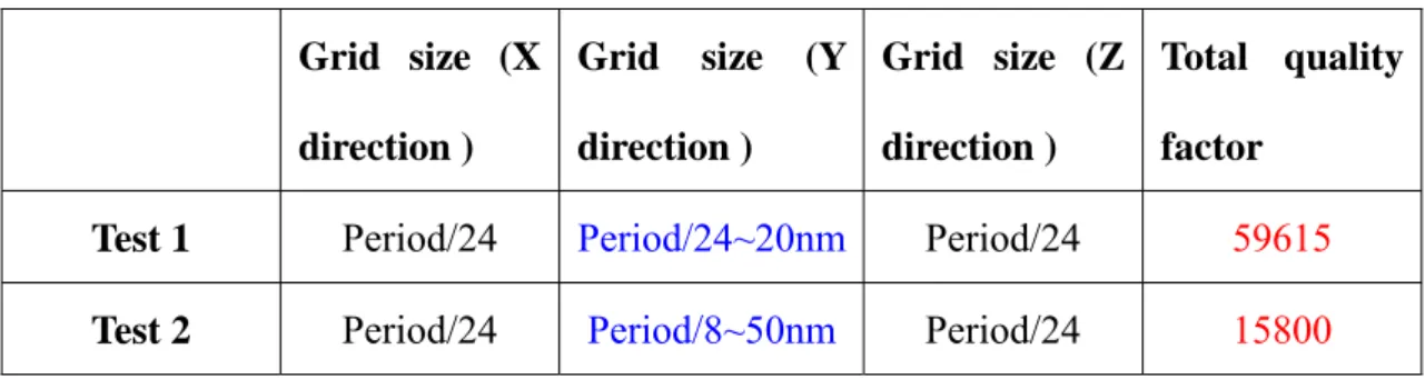
(41) (b) Fig.2-10 (a) The energy density detected by time monitor1, 2, and3 versus time duration (b) The fitted data of time monitor 1 with first order exponential decay.. From the fitting data, the calculated quality factor is given by equation (2.20) 1 = 59615 λ 1.579725 Resonant wavelength=1.579725μ m where τ p c = 14983μ m........................................2.20. Q = 2πτ p. c. = 2π ×14983. The final result is still far from the simulation result proposed in reference [3] due to the issue of grid size. But if we take fabrication tolerance into consider, this result is reasonable. The gird size used here is period/24 for X,Y, and Z directions. Table 2.1 is the comparison of quality factor between different grid size.. 30.
(42) Table 2.1 Comparison of quality factors with different grid size. Grid size (X Grid direction ). size. (Y Grid size (Z Total quality. direction ). direction ). factor. Test 1. Period/24. Period/24~20nm. Period/24. 59615. Test 2. Period/24. Period/8~50nm. Period/24. 15800. 31.
(43) 2.4.2 Quality factor for each mode existed in the double hetero-structure cavity. Now, we start to analyze quality factor for each mode existed in the double hetero-structure cavity by 3D FDTD method. All simulated parameter are listed in table 2.2. Here the grid size in Y direction is set to 44nm instead of the Period/24. It is because by carefully defining the simulation domain and the grid size in the Y direction, we can remove the grad index layer. Our slab waveguide height is 220nm which is divisible by 44, so the simulation domain in Y direction is set to 308nm which is a multiple of 44. The transverse index profile is shown in Fig.2-11, we can see that grad index layer is disappear.. Fig.2-11. The transverse index profile while grid size(Y) is equal to 44nm and simulation domain (Y) is set to 308nm. The graded-index layer is disappear.. 32.
(44) The quality factor for each mode is shown in Fig.2-12. We want to emphasize that the value of the calculated quality factor may not be a correct value due to rough grid size. But we can still distinguish relative attitude of quality factor which is not influenced by the grid size. From Fig.2-15, we can see that the mode F has the highest quality factor and the mode D is the second highest one. However, the quality factor of mode D is about a half of the quality factor of mode F. As a result, we focus our discussion on the F and D modes and we will fine tune the PC structure to let these two modes go into the gain spectrum of MQWs. The fabrication processes will be introduced in the next chapter.. Fig.2-12 The quality factor for each resonant mode.. Table 2.2 Simulation parameters. Parameter. value. Parameter. value. Material refractive index. 3.4. Grid size(X). Period/24. Air hole refractive index. 1. Grid size(Y). 44nm. Slab waveguide height. 220nm. Grid size(Z). Period/24. Period. 480nm. Simulation domain. 11μm. 33.
(45) in X direction r/a. 0.3. Simulation domain in Y direction. 220nm+88nm. Excitation source. Impulse. Simulation domain in Z direction. 9μm. 34.
(46) 2.5 Conclusion This chapter, we analyze the double hetero-structure resonant modes. We show the total electric field and show the plot of resonance mode frequency versus r/a ratio. There are seven resonance modes. In the quality factor simulation, we firstly test the accuracy of simulation method, we get a reasonable result which is approach to the real measurement result to make sure the energy decay method is applicable in Q calculation. Secondly, we use this method to calculate the quality factor for each resonant mode supported by the double hetero-structure cavity. We find that mode F has the highest quality factor and mode D is the second highest one, so we focus our discussion on these two modes and fine tune the PC structure to let these two modes go into the gain spectrum of MQWs.. 35.
(47) Chapter 3 Fabrication process for double Hetero-structure Waveguide-Resonator Here, we will introduce the fabrication processes of membrane structure and realize double hetero-structure waveguide-resonator.. 3.1 Fabrication process for membrane structure The structure of the wafer is shown in Fig.3-1. The epitaxial structure is InGaAsP/InP. multi-quantum. wells(MQWs).. Four. layer. 10nm. 0.85%. compressively-strained InGaAsP quantum wells and three layer 20nm unstrained InGaAsP barrier layers will be alternatively grown on the InP substrate. The photoluminescence (PL) spectrum of the MQWs is centered at the wavelength of 1550nm. The 60nm InP cap layer is used to protect MQWs from destruction during dry etching processes.. 60nm InP Cap layer 57.5nm Unstrained InGaAsP. PL spectrum centered at. Four 0.85% compressively-strained 1550nm. 220nm. InGaAsP QWs. (40nm) + Three. unstrained InGaAsP Barrier(60nm). 57.5nm Unstrained InGaAsP. InP substrate. Fig.3-1 The epitaxial structure of InGaAsP/InP MQWs wafer.. 36.
(48) The main fabrication processes can be divided into four steps as shown in Fig.3-2. The first step, we use plasma-enhanced-chemical-vapor-deposition (PECVD) with SiH4/NH3/N2 mixture gas to deposit 140nm SiN which is served as the hard mask layer. The second step, 300nm Polymethylmethacrylate (PMMA) is spin-coated on the SiN layer, and then JEOL 6500 electron-beam (E-Beam) lithography system is employed to defined the photonic crystal (PC) pattern. After defining the PC pattern, we use MIBK/IPA mixture solution to develop it. The third step, PC pattern is transferred into the hard mask, MQWs, InP substrate by a series of dry etching processes. We employ the Inductively Coupled Plasma Reactive Ion Etching dry (ICP/RIE) etching system to do this processes. The fourth step, we use HCl/H2O mixture solution to undercut the InP substrate at room temperature less than 4℃ for 8~16 minutes depended on the length of device and area of window. Some details of recipe for dry etching step are listed in the table 3.1. Table 3.1 ICP/RIE recipes Step. SiN etch. PMMA remove. InP etch. Gas 1 (sccm). CHF3 50. O2 100. H2 (0.8mT)~23. Gas 2 (sccm). O2 5. Cl2 (0.3mT)~18. Gas 3 (sccm). CH4 (0.4mT)~29. ICP power(W). 0. 0. 1000. RF power(W). 150. 200. 85. Pressure(mT) Temperature(℃). 55. 100. 4. 20. 20. 150. He(sccm). 0. 0. 10. Time(sec). 120. 20. 105. Depth(nm). 140nm. 300nm. ~1000nm. Note : SCCM ( Standard cubic centimeter per minute) = 0℃, 1atm, cm3/min. 37.
(49) 300nm PMMA 140nm SiN. 140nm SiN. InP Cap layer. InP Cap layer. InGaAsP Spin coating 300nm InP substrate. PMMA. InGaAsP InP substrate. E-beam define PC pattern. 300nm PMMA. 300nm PMMA. 140nm SiN. 140nm SiN. InP Cap layer. InP Cap layer. InGaAsP InP substrate. InGaAsP. RIE dry etch : transfer pattern into SiN. InP substrate. hard mask. ICP dry etch : Remove PMMA. 300nm PMMA. 300nm PMMA. 140nm SiN. 140nm SiN. InP Cap layer. InP Cap layer. InGaAsP InP substrate. InGaAsP. ICP dry etch : Transfer pattern into MQWs and InP. 38. InP substrate.
(50) ICP dry etch : Remove SiN layer. 300nm PMMA 140nm SiN Under Cut : HCl : H2O = 4 : 1. InP Cap layer InGaAsP InP substrate. Fig.3-2 A flow chart of fabrication processes for membrane structure.. 39.
(51) 3.2 CAD design and SEM picture.. We use CAD tools to layout photonic crystal pattern before E-beam lithography. In order to successfully fabricate our device with proper scale, the fabrication tolerance should be included in the CAD design. Each dry and wet etching step will enlarge the radius of air holes and the test result are listed in the table 3.2. Table 3.2 Fabrication tolerance of each dry and wet etching step E-Beam pattern. Transfer to SiN. Transfer to InP. After undercut. layer. layer. Radius of air hole. AveragedΔr. AveragedΔr. AveragedΔr. = 120~160nm. ~5nm. =10nm. <2nm. Radius of air hole. AveragedΔr. AveragedΔr. AveragedΔr. >160nm. ~5nm. >15nm. <2nm. After finishing all etching processes, the increment of diameter of air hole is roughly equal to 30nm if original radius is equal to 120~160nm after E-beam lithography. Now, we listed the fabrication parameter of our device in table 3.3. We choose three kinds of r/a ratio to match the target r/a ratio. In E-beam lithography process, the position control is more precise than the size control of air hole. Therefore, the lattice constant is directly set to target lattice constant without correction. Table 3.3 The comparison between target and fabrication parameter of our device. Target parameter. Fabrication parameter. Lattice constant(nm). 480. 480. r/a ratio. 0.3. 0.22,0.24,0.26. 40.
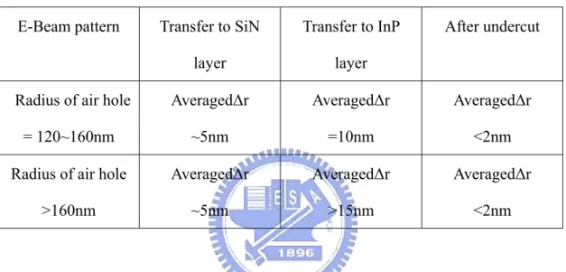
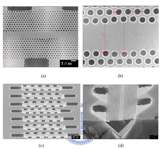
(52) .. The windows are also an important part in the cad design. We use two kinds of. windows with different size. In the input and output side of the waveguide, we put a 23μm*13μm rectangle windows in order to enhance the ratio of undercut. In the top and bottom side of the waveguide, we put smaller windows (7μm *7μm) in order to provide more support to the membrane structure. The CAD layout is shown in the Fig.3-3.. 23μm. 13μm. 7μm 7μm Fig.3-3 The CAD layout of our device.. The fabrication processes have been introduced in 1ast section. Here, we only show the SEM pictures of fabricated devices. The successfully fabricated devices are shown in the Fig3-4 (a), (b) and (c). The wet etching time is dependent on the size of the air hole and windows. As a result, some devices are successfully undercut, but others are failed at the same sample.. 41.
(53) (a). (b). (c) (d) Fig. 3-4 (a)(b) The SEM pictures of the devices with successful undercut The (c) Top view and (d) side-view SEM pictures after cutting.. 42.
(54) 3.3 Conclusion This chapter, we have introduced the fabrication processes of double hetero-structure waveguide resonator. We also discuss how to design the cad to get the device with proper scale. The devices have been successfully fabricated and the measurement results will be shown in the next chapter.. 43.
(55) Chapter 4. Measurement results. This chapter, we will show the measurement results of our devices. The measurement results are divided into two parts. One is in the vertical direction, the other one is in the in-plane direction.. 4.1 Measurement system. In order to measure both vertical and in-plane lasing characteristic of double hetero-structure waveguide-resonator. We combine the original micro PL system and a accuracy moving stage with 0.1μm resolution in space. The configuration of measurement system is depicted in Fig.4-1(a) and (b).. The TTL 845nm laser with 0.5% duty cycle is served as an exciting source. The laser beam accompanied with white light source pass through the 50/50 beam splitter, half of laser beam will go into IR camera and form the image, the other one will be focused on the sample by 100X objective lens. The emission has two directions. The vertical emission passes through the 100X objective lens in opposite direction of input laser beam, and directly goes into fiber coupler. The resonant spectrum is analyzed by the optical spectrum analyzer (OSA).. The in-plane emission is accepted from the cut facet of waveguide. We use a lens fiber to collect the in-plane emission and analyze the signal with OSA. The in-plane and vertical signal is analyzed separately.. 44.
(56) Fiber coupler Monitor. Optical spectrum analyzer (OSA) Emission Source Pumped Source. IR Camera 50/50Beam splitter. 845nm TTL laser. 100X. White Light. Objective Len. source. Moving stage. Lens Fiber. Sample. Fiber coupler. (a). (b). (c). Fig.4-1 (a) The configuration of micro PL measurement system.(b) (c) The configurations of measurement setup.. 45.
(57) 4.2 Identify the lasing mode. We firstly identify the lasing modes of all fabricated devices. We compare the measurement result with simulation one which is already shown in the Fig.2-6. The compared result is shown in the Fig.4-2. From the compared result, there are three possible lasing modes. One is mode B, another one is mode C and the other one is mode D.. Fig.4-2 Identify the lasing modes by the simulation data. There are three possible lasing modes, mode B, mode C, and mode D.. First part, in most of our devices, mode B appears with mode C when pumped power is larger than 3mW, but the output intensity is lower than that of mode C at least 10dB. In fact, we can not see correct light-in light-out curve(L-L curve) of mode B. In the other word, mode B is just a side mode. This result is agreed with the. 46.
(58) indication of quality factor simulation. The quality factor of mode B is much smaller than mode C and D.. Second part, we discuss the mode C. From section 2.4.2, the quality factor of mode C is lower than that of mode D about four times, but this difference is not so huge. All devices have only one emission peak when a/λ is between 0.31 and 0.323. Therefore, we presume that it is possible for mode C to lasing. The reasonable explanation may be that cavity boundary affects mode D much more than mode C. On the other word, if the cavity boundary is bad, the quality factor of mode D may be decreased rapidly. So, mode C has a chance to become a lasing mode. Another reason is that mode D drops out of the gain spectrum so that mode C becomes lasing mode.. Third part, mode D is the major lasing mode of our device in this fabrication. The quality factor of mode B is just smaller than mode F. We initially use 2D FDTD to estimate the lasing wavelength of each mode. We focus on the mode F and fine tune the lattice constant to let the lasing wavelength of mode F at 1.58μm. Unfortunately, the lasing wavelength of mode F with corrected lattice constant has been proven at the 1.65μm after the 3D simulation setup. As a result, the mode F drops out of the gain spectrum in our fabricated devices and mode D become the major lasing mode. The lasing wavelength of mode D between 1.54μm to 1.6μm will be single mode lasing. So the measurement result presented in the next section will focus on this wavelength region.. 47.
(59) 4.3 The lasing characteristic of mode D in both vertical and in-plane direction The lasing spectrum above threshold of device 1 which its r/a ratio and lattice constant are equal to 0.302 and 482.6nm are obtained and shown in Fig. 4-3(a) and (b). The lasing wavelength is 1543.7nm, and the side mode suppression ratio (SMSR) is 20.56dB above threshold. The threshold average power is 1.9mW as shown in Fig.4-3(c).. (a). (b). (c). (d). Fig.4-3 The vertical lasing spectrum above threshold of device 1 in (a) linear and (b) dB scale.(c)The L-L curve and (d)The SEM picture of device 1 48.
(60) The in-plane lasing spectrum above threshold of device 1 is shown in the Fig.4-4. The lasing wavelength is 1543.17nm which is agreed with the vertical lasing wavelength. The SMSR is 7.21dB above threshold. The intensity of in-plane emission is much smaller than the intensity of vertical emission due to the propagation loss within the waveguide and re-absorption of gain medium. The distance between cavity and output facet is 22.173μm as shown in Fig.4-3(d). Fig.4-4 The in-plane lasing spectrum above threshold of device 1in (a) linear (b) dB scale. The lasing spectrum above threshold of device 2 which its r/a ratio and lattice constant are equal to 0.292 and 505.3nm are obtained and shown in Fig. 4-5(a). The lasing wavelength is 1592.98nm, and the side-mode-suppression-ratio (SMSR) is 23.33dB above threshold. The threshold average power is 1.96mW as shown in Fig.4-5(c). The in-plane lasing spectrum above threshold of device 2 is shown in the Fig.4-6. The lasing wavelength is 1593.51.nm which is agreed with the vertical lasing wavelength. The SMSR is 11.41dB above threshold. The distance between cavity and output facet is 22.173μm as shown in Fig.4-5(d). The intensity of in-plane emission is better than device 1, but the threshold power is slightly larger than device 1. The possible explanation of this phenomenon may be that the in-plane loss of device 2 is larger than that of device 1, so the threshold power increases. 49.
(61) (a). (b). (c). (d). Fig.4-5 The vertical lasing spectrum above threshold of device 2 in(a) linear and(b) dB scale.(c)The L-L curve and (d)The SEM picture of device 2. Fig.4-6 The in-plane lasing spectrum above threshold of device 2 in(a) linear and(b) dB scale. 50.
(62) 4.4 Conclusion In this chapter, we compare the measurement result with the simulation one to identify the lasing modes. We also explain why the mode F drops out of the gain spectrum due to some estimation mistake. The lasing characteristic of mode D in both vertical and in-plane direction is obtained. The basic in-plane emission action is achieved. The distance between cavity and output facet of waveguide is longer than 20μm which is enough for integrating other devices.. 51.
(63) Chapter 5 Conclusion We have successfully fabricated the double hetero-structure photonic crystal waveguide-resonator and provide the quality factor of each resonance mode by 3D FDTD method. The first high Q mode is mode F which its quality factor is equal to 19000. The second high Q mode is mode D which its quality factor is equal to 8000. In measurement, we compare the measurement result with simulation one to identify the lasing mode. The major lasing mode is mode D. The mode F drops out of the gain spectrum due to estimation error and is not included in this thesis. Single mode operation can be achieved and the threshold average power of our device is about 1.9 mW from the vertical emission. The basic in-plane emission is achieved in this paper and the SMSR of in-plane emission is 7.21dB and 11.41dB above threshold.. The in-plane emission device is formed by simply shifting the six air hole position near the boundary of cavity. The distance between cavity and output facet of waveguide is longer than 20μm which is equal to 40 period. This device can be easily integrated in the optical circuit without affecting other device design and The way of vertical pumping possesses better tolerance of vibration. We believe that this device is useful in the optical communication.. 52.
(64) Reference [1] E.Yablonovitch,” Inhibited Spontaneous Emission in Solid-State Physics and Electronics” Phys. Rev. Lett. Vol. 58, pp, 2059-2062, 1987. [2] J. D. Joannopoulous, R. D. Meade, J. N. Winn, Princeton University Press, 1995. [3]. Yoshihiro Akahane, Takashi Asano, Bong-Shik Song, and Susumu Noda,. “Fine-tuned high-Q photonic-crystal nanocavity ”Optics Express. Vol. 13, No 4. pp, 1202-1214, 2005 [4]. Alongkarn Chutinan, Masamitsu Mochizuki, Masahiro Imada, and Susumu. Noda,” Surface-emitting channel drop filters using single defects in two-dimensional photonic crystal slabs” Appl. Phys. Lett. Vol. 79, No17. pp, 2690-2693,2001 [5]. Yoshihiro Akahane,a) Masamitsu Mochizuki, Takashi Asano, Yoshinori. Tanaka,and Susumu Noda,” Design of a channel drop filter by using a donor-type cavity with high-quality factor in a two-dimensional photonic crystal slab” Appl. Phys. Lett. Vol. 82, No9. pp, 1341-1344,2003 [6]. Bok-Ki Min, Jae-Eun Kim, Hae Yong Park, “Channel drop filters using resonant. tunneling processes in two-dimensional triangular lattice photonic crystal slabs”, Optics Communications, Vol. 237,pp, 59-63,2004 [7]. Hitomichi Takano,a) Yoshihiro Akahane,b) Takashi Asano, and Susumu Noda,. Appl. Phys. Lett.” In-plane-type channel drop filter in a two-dimensional photonic crystal slab”, Vol. 84, No13. pp, 2226-2228,2004 [8]. Bok-Ki Min, Jae-Eun Kim, and Hae Yong Park,” High-efficiency. surface-emitting channel drop filters in two-dimensional photonic crystal slabs”, Appl. Phys. Lett. Vol. 86, No1. pp, 011106-011108,2005. 53.
(65) [9] Hitomichi Takano, Bong-Shik Song, Takashi Asano, and Susumu Noda,” Highly efficient multi-channel drop filter in a two-dimensional hetero photonic crystal” Optics Express. Vol. 14, No 8. pp, 3491-3496, 2006 [10] Kuon Inoue, Yoshimasa Sugimoto, Naoki Ikeda, Yu Tanaka, Kiyoshi Asakawa, Taishi Maruyama, Kazuya Miyashita, Koji Ishida and Yoshinori Watanabe, “Ultra-Small. GaAs-Photonic-Crystal-Slab-Waveguide-Based. Near-Infrared. Components: Fabrication, Guided-Mode Identification, and Estimation of Low-Loss and Broad-Band-Width in Straight-Waveguides, 60°-Bends and Y-Splitters” Janpanese Journal of Applied Physics, Vol 43,pp,6112-6124,2004. [11] Attila Mekis, J. C. Chen, I. Kurland, Shanhui Fan, Pirrre R. Villeneuve, and J. D. Joannopoulos, “High Transmission through Sharp Bends in Photonic Crystal Waveguides”, Physical Review Letters. Vol. 77, No18. pp,3787-3790,1996. [12]Masaya Notomi , Akihiko Shinya , Satoshi Mitsugi , Goh Kira , Eiichi Kuramochi, and Takasumi Tanabe, “Optical bistable switching action of Si high-Q photonic-crystal nanocavities”,. Optics Express. Vol. 13, No 7.. pp, 2678-2687,. 2006. [14]Bong-Shik Song , Susumu Noda , Takashi Asano and Yoshihiro Akahane, “Ultra-high-Q photonic doubleheterostructure nanocavity”, Nature materials, Vol. 4, pp, 207-210, 2005 [15]Yoshihiro Akahane, Takashi Asano, Hitomichi Takano, Bong-Shik Song, Yoshinori Takana, and Susumu Noda, “Two-dimensional photonic-crystal-slab channeldrop filter with flat-top response”, Optics Express. Vol. 13, No 7. pp, 54.
(66) 2512-2530, 2005 [16] G. Mur, IEEE Transactions on Electromagnetic compatibility, Vol. 23, pp, 377-382,1981. [17] Emanuel istrate* and Edward H.Sarget, Reviews of Modern Physics,” Photonic crystal heterostructures and interfaces”, Vol 78 , pp455-477.. 55.
(67)
數據
+7

相關文件
6 《中論·觀因緣品》,《佛藏要籍選刊》第 9 冊,上海古籍出版社 1994 年版,第 1
(d) While essential learning is provided in the core subjects of Chinese Language, English Language, Mathematics and Liberal Studies, a wide spectrum of elective subjects and COS
Students are asked to collect information (including materials from books, pamphlet from Environmental Protection Department...etc.) of the possible effects of pollution on our
In Learning Objective 23.1, students are required to understand and prove the properties of parallelograms, including opposite sides equal, opposite angles equal, and two
Wang, Solving pseudomonotone variational inequalities and pseudocon- vex optimization problems using the projection neural network, IEEE Transactions on Neural Networks 17
Then, it is easy to see that there are 9 problems for which the iterative numbers of the algorithm using ψ α,θ,p in the case of θ = 1 and p = 3 are less than the one of the
In summary, the main contribution of this paper is to propose a new family of smoothing functions and correct a flaw in an algorithm studied in [13], which is used to guarantee
another direction of world volume appears and resulting theory becomes (1+5)D Moreover, in this case, we can read the string coupling from the gauge field and this enables us to
