國立交通大學
電子工程學系 電子研究所碩士班
碩士論文
複晶矽奈米線通道在雙閘極倒 T 型結構上之
製作與特性分析
Fabrication and Characterizations of
Inverse-T Double-Gated Devices with
Poly-Si Nanowire Structure
研 究 生:戴君帆
指導教授:林鴻志 博士
黃調元 博士
複晶矽奈米線通道在雙閘極倒 T 型
結構上之製作與特性分析
Fabrication and Characterizations of
Inverse-T Double-Gated Devices with
Poly-Si Nanowire Structure
研究生: 戴君帆 Student: Chun-Fan Dai 指導教授: 林鴻志 博士 Advisor: Dr. Horng-Chih Lin 黃調元 博士 Dr. Tiao-Yuan Huang
國 立 交 通 大 學
電子工程學系 電子研究所碩士班 碩 士 論 文
A Thesis
Submitted to Department of Electronics Engineering & Institute of Electronics College of Electrical and Computer Engineering
National Chiao Tung University In Partial Fulfillment of the Requirements
For the Degree of Master In
Electronics Engineering July 2009
Hsinchu, Taiwan, Republic of China
I
複晶矽奈米線通道在雙閘極倒 T 型結構上之
製作與特性分析
研究生:戴君帆 指導教授:林鴻志 博士
黃調元 博士
國立交通大學
電子工程學系 電子研究所碩士班
摘要
在本篇論文中,利用邊襯蝕刻技術製作具有雙閘極結構的複晶矽奈米線通道。 閘極耦合效用能有效改善基本電性與寫入/抹除特性。在奈米線通道和雙閘極結 構下,藉由增強閘極的控制能力,能有效抑制短通道效應。此外,較好的次臨界 擺幅與較大的打開電流也能因此獲得。小體積奈米線通道和雙閘極結構,在不同 操作條件下,可輕易地調控臨界電壓。以氮化矽為堆疊介電層結構下,能有效降 低漏電流。 利用雙閘極結構,研究在不同操作條件下的寫入,抹除和讀取特性。 除此之 外,本論文亦展示在此雙閘極結構中,1、0 狀態下的電壓差異與寫入/抹除效率 的調控。即便如此,可靠度特性(例如:資料保存、元件耐久性)並不如預期。穿 隧氧化層與奈米線通道結構的替代選擇,將能使可靠度獲得顯著的改善。II
Fabrication and Characterization of
Inverse-T Double-Gated Devices with
Poly-Si Nanowire Structure
Student:Chun-Fan Dai Advisors:Dr. Horng-Chih Lin Dr. Tiao-Yuan Huang
Department of Electronics Engineering and Institute of Electronics National Chiao Tung University, Hsinchu, Taiwan
Abstract
In this thesis, poly-Si nanowires(NWs) with independent double-gated(DG) configuration are fabricated by a simple sidewall spacer techniques. Gate-to-gate coupling effect facilitates the basic electrical characteristics and programming/erasing (P/E) characteristics. NWs and DG structure effectively mitigate short-channel effect by enhancing the gate controllability. Besides, better subthreshold swing and higher on-current can be achieved as well. Threshold voltage (VTH) is easily modulated in
different operating modes due to the small volume of NWs, together with the DG structure. In addition, off-state current is suppressed in the fabricated devices with O/N/O stack dielectrics.
Programming, erasing and reading under different manipulation of the DG structures are studied. In addition, VTH windows and modulation of the P/E efficiencies with DG
structure are demonstrated in this study as well. However, the reliability characteristics (i.e., retention, endurance) are poorer than expected. Substitutes for tunneling oxide dielectrics and alternatives to the NW structures are needed in order to achieve better the reliability characteristics.
III
誌謝
研究生生活即將在此告一段落,很開心能夠成為先進元件實驗室的成員之一。 最令人回味的莫過於實驗室融洽且歡熱的氣氛,從碩一到碩二的日子以來,承蒙 老師,學長姐,與學弟妹的關照與照顧,只能說先進元件實驗室是交大電子所中 最幸福的實驗室。首先,特別謝謝林鴻志老師與黃調元老師的指導,對老師感謝 的心不會隨著時間而消逝;嚴謹中不失和氣的領導風格,其中不乏對學生的支持, 在這近乎百分百開放自由的環境之下,培養我們對自己負責的能力。首先要非常 謝謝 NDL 的趙子綾小姐,謝謝妳,讓我在元件製作上能很順利地完成。另外更要 感謝博班學長群:林哲民,徐博,蔡子儀,大師,林政頤和馬卡。首先要感謝我 的實驗大助教-徐行徽學長,如果沒有你在實驗上的把關,現在的我應該在開學 前都還在趕著寫論文;謝謝陳威臣學長在物性實驗上的幫忙,並且在關鍵時刻上 分享電性結果。豔陽般熱情的蔡子儀學長,進入實驗室後,你是我第一個感受到 學長的熱情與活力,負責打理實驗室大大小小的事,辛苦了,也謝謝你熱心幫我 取了很多食物的綽號。認識快六年的馬卡同學與笑聲很有特色的林政頤同學,資 格考 pass pass pass;以上,希望博班都能順利快樂畢業。接下來,要特別謝謝同進同出的碩二夥伴們:育嘉,瑄勻,維濤,政建,佑 寧,格綸,瑞傑。同時扮演同學,室友兼朋友角色的育嘉,謝謝妳一路以來的陪 伴;謝謝格綸在這兩年中,為實驗室辦的活動,讓我們能帶著滿滿的回憶畢業。 另外,謝謝已經畢業的 95 學長姐,謝謝給予一起出遊、唱歌,修課的回憶,謝 謝你們熱情地參與我們 96 的共同回憶。也祝升碩二的 97 的大家身實驗順利,健 康幸福。 謝謝弘森,因為有你,讓我能追尋屬於自己的勇氣!!! 最後,感謝我家人的支持,讓我能百分百享受屬於自己的人生。 2009.7
IV
CONTENTS
Chinese Abstract……….………Ⅰ English Abstract………..……... Ⅱ Acknowledgement……….………...…………..…. Ⅲ Contents……….………….………...…...….... Ⅳ Figure Captions………...…….………. Ⅵ CHAPTER 1 Introduction1-1 Overview of Nanowire and Multiple-Gate Technology……….…..1
1-2 Overview of SONOS-Type Memory Devices...………..3
1-3 Motivation ………...…………...………4
1-4 Thesis Organization………..…………...5
CHAPTER 2 Device Structure, Fabrication, and Operation 2-1 Device Structure and Process Flow………....…………...6
2-2Short Channel Effect………...7
2-3 Program and Erase Mechanisms for NVM Device Operations ………..8
2-3-1 Channel Hot Electron Injection………..8
2-3-2 Tunneling Mechanisms………....………...9
2-3-2-1 Fowler-Nordheim Tunneling (FN)………..10
2-3-2-2 Direct Tunneling (DT)……….10
2-3-2-3 Modified Fowler-Nordheim Tunneling (MFN)………...11
2-3-2-4 Trap-Assisted Tunneling (TAT)………...11
2-3-3 Band-to-Band Tunneling (BTBT)………..………..……12
V
2-4-1 Retention………...………...12
2-4-2 Endurance………...…….……….14
CHAPTER 3 Results and discussion 3-1 Previous Remark………...………..…..……….16
3-2 DG-NW-TFT………...…..………...…………...17
3-2-1 Electrical Characteristics………...….………..17
3-2-2 Leakage Current………..…...18
3-2-3 VTH Modulation under Independent Double-gated Operation…...20
3-3 DG-NW-SONOS…...21
3-3-1 Program and Erase Characteristics………...21
3-3-2 Reliability Characteristics……….……….22
3-3-2-1 Retention……….22
3-3-2-2 Endurance………23
CHAPTER 4 Conclusions and Future Work 4-1 Conclusions………...25
4-2 Future Work...26
References………...27
VI
FIGURE CAPTIONS
CHAPTER 2
Fig. 2-1 Top view and cross-sectional view of the inverse-T double-gate NW-SONOS device.………..………..……....….35 Fig. 2-2 (a) Deposition of the n+-doped poly-Si (b) After removal of 100nm-thick n+-doped poly-Si in all regions except the central height of IVTG (c) After removal of the remaining 50nm-thick in-situ doped n+ poly-Si in all regions except the IVTG, leaving the final IVTG (d) Deposition of inverse-T O/N/O stack and ploy-Si active layer (e) Source/Drain ion implantation (f) Definition of nanowire channel and source/drain (g) Deposition of the upper O/N/O stack and top gate………..……….….35-39 Fig. 2-3 Dependence of the threshold voltage on channel length and drain bias.………..……….40 Fig. 2-4 Illustration of channel hot electron injection (CHEI) showing that under large drain bias, some channel electrons could become hot enough to surmount the Si/oxide barrier………...40 Fig. 2-5 (a) Illustration of F-N tunneling occurring when Vot is larger than υb (b)
Illustration of direct tunneling occurring when X∅𝑏
ot> |Eot |>
∅b−∅n
xot , where
Eot is the electric field across the tunneling oxide (c) Illustration of Modified
F- N t unn el i n g o c cu rri n g wh en n∅bx−∅n
ot > Eot >
∅b−∅n
xot+ εox xεn n
( d) Illustration of trap assisted tunneling occurring when ∅b−∅xn−∅t
VII
∅b−∅n−∅t
xot+ εox xεn n ……….……41-42
Fig. 2-6 Illustration of band-to-Band tunneling (a) Deep depletion occurs in the gate-to-drain overlap region when there is a significant voltage drop across the gate and drain. (b) Tunneling paths in the deep depletion region…..…43 Fig. 2-7 Data lost paths of SONOS flash memory……….……..………..44
CHAPTER 3
Fig. 3-1 Cross-sectional TEM images of an ITG NW-TFT…………....…………...45 Fig. 3-2 (a) Transfer and (b) output characteristics of the ITG NW-TFT…………..46 Fig. 3-3 On-current as a function of channel length under different operation modes………...47 Fig. 3-4 Off-current with different dielectrics conditions under different operation
modes.…...………...47 Fig. 3-5 Leakage under overlapped region of gate and drain via BTBT…………...48 Fig. 3-6 (a) Top view of DG-NW-SONOS. Off-current as a function of (b) top width operated in ITG mode and (c) bottom width of ITG operated in TG mode……….49 Fig. 3-7 Leakage path in (a) ITG mode of operation and (b) TG mode of operation………50 Fig. 3-8 Transfer characteristics under varying auxiliary gate bias for (a) ITG mode and (b) TG modes of operation. VTH variation as a function of auxiliary gate
VIII
Fig. 3-9 Transfer curves under different P/E conditions………...52 Fig. 3-10 Voltage drop across nitride/oxide/Si on the side of the auxiliary gate under programming operations. Solid and dashed lines represent the potential profiles when the auxiliary gate is grounded, and biased positively, respectively………...52 Fig. 3-11 (a) Program efficiency under different programming conditions. (b) VTH
shift as a function of the top gate bias for the programming operation…...53 Fig. 3-12 (a) Erase efficiency under different erasing conditions (b) VTH shift as a
function of the top gate bias for the erasing operation……….…54 Fig. 3-13 Voltage drop across nitride/oxide/Si on the side of the auxiliary gate under programming operations. Solid, dashed, and dotted lines represent the potential profiles with the auxiliary gate grounded, biased positively, and biased negatively, respectively……….55 Fig. 3-14 Voltage drop across nitride/oxide/Si on the side of the auxiliary gate under erasing operations. Solid, dashed, and dotted lines represent the potential profiles with the auxiliary gate grounded, biased positively, and biased negatively, respectively………...………….55 Fig. 3-15 Retention characteristics (a) transfer curves and (b) VTH shift with time....56
Fig. 3-16 Schematic illustration of nitride trapped electrons escape by Frenkel-Poole emission and subsequent oxide trap-assisted tunneling………...57 Fig. 3-17 Schematic illustration of the escaped path of tunneling oxide (TO) trapped holes in the erased state………57 Fig. 3-18 (a) Transfer characteristics and (b) VT H variation with cycling
IX
Fig. 3-19 Schematic illustration of postulated distribution of trapped electrons in nitride layer after programming. Owing to the higher electric field with a larger curvature, more electrons are trapped in the nitride near the corners………59
1
CHAPTER 1
Introduction
__________________________________
1-1 Overview of Nanowire and Multiple-Gate
Technology
In 1965, Gordon Moore predicted that the computing power and the number of the transistors on the chip will double roughly every two years [1-1]. Since then, Moore’s law has been a reliable instruction to the development of electronic technology. From the 1970’s, silicon integrated circuits have become indispensable and ubiquitous to our lives. Over the last thirty years, continuous efforts have been kicked into gear in the miniaturization of electronics [1-2], leading to the Information Age for 21st –century society.
With the scaling of the devices, consumer-electronic appliances make tremendous progress in functionality, productivity, and power efficiency. At the same time, as a result of electrostatics and parasitic phenomena, the scaling reduction seems to face its bottleneck. Feeble electrostatic gate control of the channel region resulting from short channel effect (SCEs) such as VTH-rolloff, sub-threshold swing
(SS) degradation and drain-induced barrier lowering (DIBL) becomes a serious issue. With a view to solve the problem, there are considerable researches on nanowire (NW) [1-3] and multiple-gate (MG) [1-4, 1-5] structures.
NW structures
2
range of functionality. Nowadays, NW channel using conventional processes show high performance with strong gate control even in the ultimately scaled paradigm. NWs enable lower leakage current, higher mobility, and better SS with merit of small volume, large surface-to-volume ratio, fewer defects and grain boundaries. Applications of NWs can be classified into two parts. One is the high-performance electronics, like dye-sensitized solar cell [1-6], label-free, ultra sensitive bio-[1-7,1-8] and chemical sensor [1-9, 1-10], and memory devices [1-11]. The other part is on-chip photonic devices and circuits, such as lasers [1-12, 1-13, 1-14, 1-15], active waveguides [1-16, 1-17] and integrated electro-optic modulators. [1-18]
For large-scale integrated circuits, the NW must possess reproducible electronic property with high yield. There are two distinct approaches for preparing NWs: “top-down” and “bottom-up.” In the top-down approach, NWs are patterned by a combination of lithography [1-19], deposition, and etching while the processing equipment and techniques cost a fortune. With each new level of manufacturing facility, the improvements of the resolution are connected to a near-exponential increase in cost. Nevertheless, the top-down approach itself can provide the accurate position for high yield. Tools of the top-down approach contain a number of advanced nano-lithographic techniques on beam-based methods, such as electron beam (e-beam)[1-20]or focused-ion-beam (FIB), proximal probe patterning [1-21], X-ray or extreme-UV lithography [1-22].
For bottom-up approach, general methods suitable for all solid materials involve vapor phase [1-23], vapor-liquid-solid [1-24], solvothermal [1-25], and the like. The main drawback is that it is difficult to control structural
3
parameters such as NW’s diameter, length, and orientation.
Multiple-gate structures
Base on the Brew’s scaling theory [1-26], high doping concentration reducing the depletion depth in the substrate must apply to bulk MOSFETs to mitigate short-channel effect (SCE). For example, the doping concentration must be higher than 1018 cm-3 for sub-100nm scale gate length [1-27], accompanied by decreased mobility and increased junction capacitance.
Multiple-gate configurations with ideal SS, high trans-conductance, and SCE immunity can circumvent the scaling limits of the bulk MOSFETs. Specifically, multiple-gate configuration can effectively suppress the penetration of electric field from the drain side into the channel. Therefore, a multiple-gate with NW channels has high robustness on SCE immunity and shows superior scalability [1-28, 1-29, 1-30, 1-31, 1-32, 1-33, 1-34].
1-2 Overview of SONOS-Type Memory Devices
In the mid-1960s, semiconductor memories based on metal-oxide-semiconductor (MOS) technology took the place of magnetic core memories in the ascendant with superior density and functionality. Owing to the drawback of volatility using MOS concept in the beginning, the solutions to the problem were the floating gate (FG) structure [1-35] and the metal-nitride-oxide-semiconductor (MNOS) memory device [1-36] proposed in 1967. Since then, the possibility of non-volatile (NV) MOS memory devices became a reality.
With the continuous scaling of the NV memory for high density/low cost, good reliability, and low programming/erasing operation voltages, several issues [1-37]
4
emerge due to inter-floating gate capacitive coupling (cell to cell interference) and tunnel oxide thickness (poor reliability due to large stress-induced leakage current (SILC)). In contrast, nitride-trapping devices with intrinsic better endurance and absence of erratic bits are invulnerable to the further scaling limits [1-38]. By virtue of the replacement of the storage layer (from poly-silicon to nitride layer), we see a seam in this field that the SONOS-type memory device is one of the most attractive candidates to address the above-mentioned issues.
Being grounded on the high density/low bit cost requirements, realizing high-speed programming and low power consumption without aggressively scaling devices for future applications in portable handheld electronic products- mass storage media like memory cards, audio/video players, to name just a few, there are two approaches that have been studied. One is the multi-bit operation technology which can be divided into two parts- multi-level cell (MLC) and multi-storage node cell (MSNC) [1-39, 1-40, 1-41, 1-42, 1-43]. The other one is 3-D structures, 3-D programmable erasable non-volatile cylindrical (PENCIL) Flash EPROM and a floating channel type surrounding gate transistor (FC-SGT) Flash Memory, for instance.
1-3 Motivation
According to the experience of the previous research in our lab (Advanced Device Technology Lab., ADTL), NWs seem to repay our time and effort. Once again, we employ the top-down technique to form sidewall spacers as the channel. With the aim of improving the device performance, we expect to have an isosceles triangle channel with small volume and DG structure for further gate controllability and modulation.
5
In addition to the NW thin-film transistor (TFT), the SONOS device is one of the possible choices of replacing FG-NVM by having low Program/Erase operation voltages and showing large compatibility with the standard CMOS process [1-44]. In order to consistently outperform the SONOS device, we have a shot at the mentioned advantages in the previous sections, NWs and MG configurations, both of which would increase P/E efficiency and decrease power consumption by suppressing SCE and gaining more control over the channel.
1-4 Thesis Organization
In Chapter 1, NWs, DG and memory devices are discussed. After that, we will briefly introduce the device structures, process flow, and the basic concepts of the SONOS memory devices in Chapter 2. Going on with the measured data consisted of basic electrical and SONOS memory characteristics in Chapter 3. Last, Chapter 4 will end with the conclusion and future work of this study.
6
Chapter 2
Device Structure, Fabrication, and
Operation
__________________________________
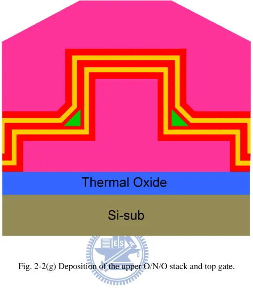
2-1 Device Structure and Process Flow
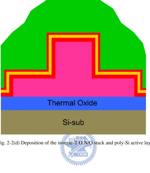
The top view of the inverse-T double gate NW SONOS and the cross-sectional view along line AA′ in the top-view structure are illustrated in Fig. 2-1. It can be seen that an ONO stacked layer was deposited on the inverse-T gate (IVTG) and/or on the surface of the NW channels, followed by the covering of the top gate (TG). The schematic process flows of the proposed device are shown in Figs. 2-2 (a) to (g). In the beginning of the fabrication, a 100nm silicon dioxide layer was deposited on 6-inch silicon wafers. This was followed by the deposition of a 150nm-thick n+-doped poly-Si which was patterned to form the IVTG by twice applying the I-line lithography/dry etching steps (Fig. 2-2 (a) to (c)). Specifically, the first etch step removed 100nm-thick n+-doped poly-Si in all regions except the central height of IVTG (Fig. 2-2 (b)). While the second etch step removed the remaining 50nm-thick in-situ doped n+ poly-Si in all regions except the IVTG, leaving the final IVTG (Fig. 2-2 (c)). Next, either a 15 nm-thick dielectric oxide or an O/N/O stack acting as the storage site was deposited by low-pressure-chemical vapor deposition (LPCVD), followed by the deposition of a 100nm-thick amorphous-Si layer by LPCVD, and continued on an annealing step at 600 ℃ in N2 ambient for 24-hour to transform the
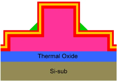
amorphous-Si into poly-Si (Fig. 2-2 (d)). Source/drain (S/D) implant was then performed via P+ implantation at 20 kev and 1E15 cm-2(Fig. 2-2 (e)). With the
7
formation of the S/D photo-resist patterned by an I-line stepper lithography, an anisotropic plasma etching was executed to form the NW channels together with the S/D definition (Fig. 2-2 (f)). It is worth noting that the channel size can be controlled by adjusting the over-etch time. This is followed by the deposition of either a 20 nm-thick dielectric oxide or an O/N/O stack. Then, a 100nm-thick in-situ doped n+ poly-Si was deposited and patterned to serve as the top gate electrode (Fig. 2-2 (g)). All devices were then capped with 250nm-thick LPCVD oxide passivation layer. Finally, contacts holes and test pads were formed using standard metallization steps.
2-2 Short-Channel Effect
The short-channel effect (SCE) refers to the decrease of the threshold voltage with decreasing channel length (i.e., VTH roll-off, as shown in Fig. 2-3), and can be
attributed to the depletion widths of the source and drain approaching the channel length. For a long channel device, the constant-potential contours are nearly paralleled along the channel length direction in most part of the channel. In other words, the electric field is one dimensional. In contrast, for an aggressively scaled device, the potential distribution becomes curvilinear throughout the channel region, so the electric field becomes two dimensional. This results in more bend bending at channel surface and, consequently, a lower threshold voltage. The higher drain bias is, the more significant SCE is, owing to the drain-induced barrier lowering effect [2-1]. Several scaling rules have been proposed. The follow expression having flexible scaling factors without being scaled by the same scaling factor κ for minimum channel length where long-channel behavior can still be observed follows a simple empirical relation [2-2]:
8
Lmin ≥ C1[rjd(Ws + WD)2]1 3 , ( eq. 2-1) where C1 is a constant, and Ws + WD is the sum of the source and drain depletion widths in a one dimensional abrupt junction formulation.
2-3 Program and Erase Mechanisms for NVM
Device Operations
The basic operating principle to switch the SONOS device between two distinct states of VTH is the storage of charges in the dielectric layer. Charges can be trapped
or de-trapped in the isolated traps in the nitride of SONOS via mechanisms like channel-hot-electron injection (CHEI), Fowler-Nordheim Tunneling (FN-tunneling), and band-to-band tunneling (BTBT). The three mechanisms will be described in the following sub-sections.
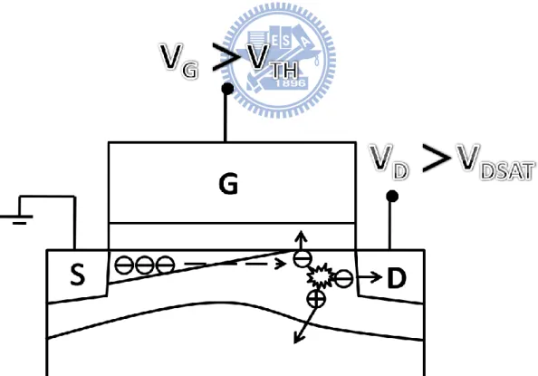
2-3-1 Channel Hot Electron Injection
As illustrated in Fig. 2-4, under large drain bias, conduction electrons in the channel gain enough energy by the large electric fields at the drain side when pinch-off starts to occur, i.e., VDS≧VDS,Sat=VG-VTH.
When sufficiently positive voltages are applied to the gate and drain while the source is grounded, electrons are accelerated by lateral electric field. With the passage from the channel to drain, the energy of conduction electrons becomes high which may give rise to impact-ionization at the drain side, by which additional electron/hole pairs are created. The electrons will drift to the drain while the holes will drift to the substrate and be collected by the substrate contact. In the mean time, portions of the electrons become hot enough to
9
surmount the tunneling oxide energy barrier and may get trapped inside the gate dielectric [2-3, 2-4].
The current density of CHEI is expressed as [2-5]: ICHEI = AdIds(λEm
υb )
2exp(−υ
b Emλ) , ( eq. 2-2)
where Ad is the scattering probability,υb is the barrier height,Em is the
channel electric field at the drain end.
Three models are commonly used to described the gate current due to CHEI: 1. The lucky electron model [2-6, 2-7] expresses that when the electrons gain
enough energy by the large lateral electric field through collisions, it may inject into the gate insulator.
2. The effective electron temperature model [2-8] suggests that electrons of the channel current are hot with electrons gas of Maxwellian distribution, assuming that the effective temperature, Te, is dependent on the electric field. The heated electrons will overcome the interface barrier through thermionic emission.
3. The physical model [2-9] calculates the gas current with the aid of accurate solution of the 2-D electric field distribution of the channel near the drain side.
2-3-2 Tunneling Mechanisms
The tunneling is based on a quantum mechanical tunneling mechanism through the oxide layer, which in fact is a field-assisted electron tunneling mechanism. The process is important for P/E operation of a NVM device. The main programming mechanisms based on the tunneling process can be
10
divided into four types, namely, F-N tunneling (FN), direct tunneling (DT), modified F-N tunneling (MFN), and trap-assisted tunneling (TAT), depending on the oxide field and oxide thickness, and the traps in the nitride.
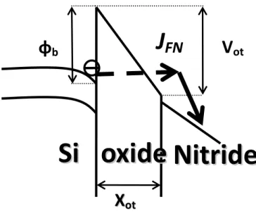
2-3-2-1 Fowler-Nordheim Tunneling (FN)
When Eot >x∅b
ot (or Vot > 𝑞∅b), where Eot is the oxide field, xot is
the oxide thickness, ∅b is the barrier height at Si /SiO2 interface, and Vot
is the voltage drop in oxide, channel electrons will tunnel into the conduction band of the oxide through triangular potential barrier by F-N tunneling as plotted in Fig. 2-5(a), and will then be accelerated by high electric field and injected into the gate. The F-N tunneling current is given by [2-10]: JFN = AEot2 e −B Eot , (eq. 2-3) where A = q 3 8πhυb m m∗,B = 8π 2m∗ υb32
3hq,and Eot=the electric field at the
injection interface
2-3-2-2 Direct Tunneling (DT)
If the electric field across the tunneling oxide (Eot) is smaller than ∅𝑏
Xot (Vot < q∅b) and larger than
∅b−∅n
xot (This is especially paramount in
ultra-thin oxide(<3nm)) , channel electrons with energy corresponding to the forbidden gap region of the insulator will tunnel their way into the allowed states of the opposite gate, where the tunneling barrier is trapezoidal as illustrated in Fig. 2-5(b). The direct tunneling current can
11
be expressed as [2-11]
JDT = AEox2 P
ox , (eq2-4)
where Pox represents the tunneling probabilities through the oxide barriers, and is given by Pox=exp{
−4
3h 2qmox∗ ∅
b32-(∅b-Eoxxot)32
Eox }.
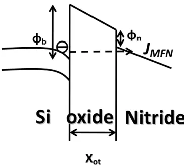
2-3-2-3 Modified Fowler-Nordheim Tunneling
(MFN)
When∅bx−∅n
ot > Eot >
∅b−∅n
xot+ εox xεn n
, channel electrons will tunnel through the oxide barrier and nitride barrier as shown in Fig. 2-5(c). The Modified Fowler-Nordheim current is expressed as [2-11]
JMFN = AEox2 PoxPn , (eq. 2-5)
where A is a constant characteristic of Modified F-N tunneling , Eox is the field across oxide,Poxis the tunneling probabilities through the
oxide barriers,Pnis the tunneling probabilities through the nitride barriers, and is given by Pn=exp{
4
3h 2qmn∗ (∅
b−∅n-Eoxxot)32
En }.
2-3-2-4 Trap-Assisted Tunneling (TAT)
For small oxide thickness and electric field, namely, ∅b−∅xn−∅t
ot >
Eot > x ∅b−∅n−∅t
ot+ εox xεn n
, channel electrons tunneling through the oxide and part of the nitride can be conspicuous, as shown in Fig. 2-5 (d) [2-12]. The time constant of the empty trap is smaller than that of the filled trap, so the channel electrons can continue to be injected into the conduction
12
band (CB) of the nitride layer.
2-3-3 Band-to-Band Tunneling (BTBT)
With a highly negative voltage relative to the drain applying to the gate, band-to-band tunneling (BTBT) contributing to the so called gate-induced drain leakage (GIDL) occurs in the deep depletion underneath the gate-to-drain overlap region, as plotted in Fig. 2-6. The BTBT current density is expressed as [2-13]
JBTBT = 2m∗q3εVDG πh2E g 1 2 exp − 8π 2m∗E g 3 2 3qεh , (eq.2-6)
where is the electric field, Eg is the energy bandgap, VDG is the voltage
difference between the drain and gate.
2-4 Reliability Issues
2-4-1 Retention
Retention is the capability of having the distinct information for a period of time without losing the stored charges in the trapping layer. The data retention specification for commercially available products is typically 10 years after programming, either during operation or with power turned off. Trapped charges establishing an electric field in the nitride layer can escape from the trapped state via the following tunneling processes as illustrated in Fig. 2-7 [2-14]:
(1) Thermal excitation emission:Trapped electrons being thermally excited to the nitride CB, followed by electron tunneling from the nitride CB to the Si
13
substrate CB.
(2) Trap-to-band (T-B) tunneling [2-15]:Electrons directly tunnel from nitride traps into the conduction band of Si substrate, namely.
(3) Trap-to-trap (T-T) tunneling [2-16]:Electrons tunnel from nitride traps into the Si/SiO2 interface traps.
(4) Band-to-trap (B-T) tunneling: Holes tunnel from the silicon valance band to the nitride traps and recombine with trapped electrons.
(5) The Poole-Frenkel emission: Trapped electrons hop from one step to another.
(6) Trap-to-gate (T-G):Stored electrons and holes tunnel through the blocking oxide to the gate electrode.
These six processes which cause losses in the storage capability for the SONOS device can be divided into two categories. The first category is the processes that are temperature insensitive, like Processes (2), (3), (4), and (6). Under the effect of the internal self-built electric field, Processes (2) and (3) are referred to as the “back tunneling” processes. With a large amount of charges stored in the nitride, Process (4) becomes a great concern and is noted as soft erase.
The second category is those processes that are temperature dependent, like Processes (1) and (5). Trapped electrons may de-trap in the bulk nitride by Poole-Frenkel emission and experience an alternation of the internal charge distribution. Furthermore, trapped electrons can also be thermally excited out of the nitride trap to the CB of the nitride at elevated temperatures, and drift toward the tunnel oxide, followed by a subsequent tunneling to the Si substrate. For conventional metal-oxide-nitride-silicon (MNOS), owing to the
14
relative thick nitride layer (about 100nm), charge redistribution resulting from hopping from one step to another, namely. Poole-Frenkel emission is an important retention loss mechanism. To date, with the development of SONOS devices, the movement of the charge is blocked by a blocking oxide, which resulting in a much thinner (5-10nm) nitride layer. For this reason, we can overlook the electron retention loss caused by Poole-Frenkel effect in scaled SONOS devices.
The time constants of the electron T-B, B-T, and T-T tunneling all follow the similar equation given by
τT(x, υT) = τ0∙ exp(αox ∙ αot) ∙ exp(αn ∙ x), (eq. 2-7)
where τ0 is a time constant for the traps, qυT is the trap energy (eV) referenced to the CB edge in the nitride, xot is the thickness of the tunnel oxide, and x is the distance from trap in nitride to tunneling oxide.
The time constant of electron de-trapping through thermal excitation is given by τTE T, υT = (AT2)−1exp(qυT kBT), (eq2-8) where A = 2σn m3kB n ,e ∗ ( 2πmn,e∗ kB
h2 )3 2, T is the absolute temperature (K), kB
is Boltzmann’s constant, and σn is the capture cross-section of the nitride traps.
2-4-2 Endurance
Endurance is the number of P/E cycles that the memory can withstand with the acceptable P/E window. The cycling performing with a high electric field is known for causing degradation of the tunnel oxide by generating more
15
oxide traps and interface traps in the tunnel oxide. Stored data can lose with the help of the defects by traps-assisted tunneling. There is a trade-off between P/E speed and highly applied electric field. Thanks to the development of the high-density memory, the number of endurance requirement decreases from 106 P/E cycles for typical application to 104 P/E cycles.
16
Chapter 3
Results and Discussion
__________________________________
3-1 Previous Remark
The electrical characteristics of the fabricated devices here were characterized by a measurement system composed of HP-4156 parameter analyzer, Agilent-E5250A switch, and Agilent-8810A pulse generator, together with Interactive Characterization Software (ICS).
The definitions of device parameters extracted for DG-NW-TFT and DG-NW-SONOS devices are briefly expressed below.
1. Subthreshold Swing(SS):
SS is calculated from the subthreshold current in the weak inversion region, expressed as
SS =∂(log I∂VG
D) , (eq.3-1)
2. Threshold Voltage(VTH):
VTH using the constant current method is defined as the gate voltage (VG) with a
specific drain current, expressed as
VTH = VG@ID = WL × 10nA , (eq.3-2) where W and L are channel width and length, respectively.
3. On-current (ION) and off-state leakage current induced by GIDL effect:
In this study, ION is the maximum drain current in the ID-VG curve when the
sweeping gate voltage equals to 5 V and the drain voltage equals to 0.5 V. While IGIDL is the drain current at the minimum sweeping gate voltage (i.e., -4 V) in the
17
ID-VG curvewith drain voltage fixed at 3V.
DG-NW devices were performed in different operating modes, that is, the inverse-T gate (ITG) mode, top gate (TG) mode, and inverse-T double gate (ITDG) mode. ITG mode refers to the state where the sweeping voltage is applied to the ITG with TG grounded. TG mode refers to the mode while TG is being swept by the applied voltage and ITG is grounded. Finally, ITDG mode refers to the condition when the sweeping voltage is applied to both ITG and TG.
3-2 DG-NW-TFT
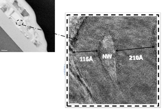
3-2-1 Electrical Characteristics
The cross-sectional transmission electron microscopic (TEM) images of a fabricated device are shown in Fig. 3-1 where the NW channel is in the shape of triangle with the dielectric thickness of ITG and TG equaling to 115 Å (denoted as TITG = 115 Å ) and 210 Å (denoted as TTG = 210 Å ), respectively. The transfer and
output characteristics of an ITDG-NWTFT are shown in Fig. 3-2, revealing that ITDG mode outperforms the others in electrical characteristics with SS amounting to 120 mV/decade and excellent on-current. From Fig. 3-2(a), ITG mode shows much better SS (SS ITG = 171 mV/decade) than TG mode (SS ITG = 240
mV/decade) mainly owing to the difference between the thickness of dielectrics. Still, with the formation of the NW channel by dry etching, plasma damage along the sloping edge of the NW channel next to the TG could be another factor degrading the performance of the TG mode. Figure 3-2(b) further displays that the two current ratios, i.e., ID, ITDG/ID, ITG and ID, ITDG/ID, TG, increase as the drain bias
18
as the drain voltage increases.
A phenomenon known as “volume inversion [3-1]” can occur when the channel is thinner than the maximum depletion width. As the channel body is sufficiently thin, an interaction between the two gates may also help reduce the potential barrier height in the conduction channel [3-2]. These two factors are the possible reasons responsible for an increase in drain current when switched from single-gate mode to double-gate mode.
In Fig. 3-3, ITDG, ITG, and TG modes are performed on the fabricated devices with different channel lengths. For all of the operating modes, the on-current is decreased when the measurement is conducted on devices with a longer channel. The trends basically follow L-1 as expected. However, as can be seen in the figure, the on-current of ITDG mode is larger than the sum of ITG and TG modes. This is attributed to the coupling effect of the two gate bias which may result in an increase in electrons density and the lowering of barrier height.
3-2-2 Leakage Current
Fig. 3-4 shows the leakage currents under different operating modes for three splits of devices with various conditions of dielectrics. In the figure the leakage current was measured at VD = 3 V and VG = -4 V. Obviously, the devices with
O/N/O shows suppression of the gate induced drain leakage (GIDL). According to the chemical reaction of the silicon nitride (Si3N4) formation by LPCVD:
19
sufficiently high in LPCVD, the silicon nitride layer is found to be non-stoichiometric with abundant of hydrogen species [3-3]. In the following steps portions of the hydrogen may diffuse into the poly-Si and passivate the defects at grain boundaries and inside the grains. GIDL due to Band-to-band tunneling has been identified as the major conduction mechanism of the leakage in the NW devices [3-4]. In this regard the existence of defects in the poly-Si facilitates the tunneling leakage via trap-assisting process, as presented in Fig, 3-5. The aforementioned passivation effect may thus help reduce the leakage, as shown in Fig. 3-4.
To further identify GIDL, relations between top width of ITG (TW-ITG) /bottom width of ITG (BW-ITG) and GIDL are shown in Fig. 3-6 where BW-ITG refers to the bottom planar width of the ITG’s (Fig. 3-6(a)) Fig. 3-6 (b) and Fig3-6(c) show the leakage measured at VD = -4 V and VG = 3 V as a function of the above-defined
structural factors. Note that the data have been normalized with respect to the devices with 0.5 µm - TW-ITG in Fig. 3-6 (b) and 1µm -BW-ITG in Fig. 3-6(c). These results indicate that the leakage is roughly proportional to the overlap width, indicating that the major conduction occurs in the overlap region between the drain and gate. Thin dielectrics that lead to a high electric field and the lightly-doped dopant profile tend to deplete drain easily, accompanied by band-to-band tunneling either-with or without the assistance in traps. As stated in Chapter 2, a low-energy implant (15 keV) was performed to avoid excess dopants being incorporated in the NW channels. Nevertheless, this results in a gradient dopant distribution in the drain region and the insufficient doping occurs in the regions (offset region) close to the NW channels and the top of the hardmask capping the ITG. Under the ITG mode of operation, electric field of the drain attracts the leakage current to flow upward the in-between space where the offset region between n+ doping region and the channel
20
region is not gated by ITG, as indicated in Fig. 3-7(a). On the contrary, the in-between offset region is gated by top gate under TG mode, so that the leakage is more susceptible to the change of the BW-ITG, as indicated in Fig. 3-7(b).
3-2-3V
THModulation under Independent Double-gated
Operation
To take advantage of the independent double-gated structure, the threshold voltage of an operation could be modulated by applying a tunable bias to the non-sweeping gate (i.e., auxiliary gate) while a sweeping voltage is applied to the other (i.e., driving gate). Figs. 3-8(a) to (b) illustrate the ID-VG characteristics under
ITG (with ITG serving as the driving gate) and TG (with TG serving as the driving gate) modes, respectively. The extracted VTH of each curve in Fig. 3-8(a) is plotted as
a function of top-gate voltage in Fig. 3-8(c). Similarly, VTH as a function of inverse-T
gate voltage from Fig. 3-8(b) is shown in Fig. 3-8(d). In the figures we can see that the approximately linear relations are achieved in Figs. 3-8(c) and (d). This is an indication of strong gate-to-gate coupling as NW is sufficiently thin [3-5]. Note that the slope in the plot can be regarded as a measure of the capability of the auxiliary gate bias in modulating the threshold voltage. In this regard, when the two figures are further compared, it’s obvious that VTH is modulated more effectively by ITG, due to
the thinner dielectric near ITG (Fig. 3-1). Thinner dielectrics represent a better or predominant potential control than the relative thick dielectrics. A substantial amount of VTH adjustment is thus expected when a tunable voltage is applied to the
gate with thinner dielectrics.
21
3-3 DG-NW-SONOS
3-3-1 Program and Erase Characteristics
Independent DG operation and NW structures can assist P/E with the merit of the strong gate-to-gate coupling effect. Fig. 3-9 shows the P/E memory window under different conditions of P/E operation. In the figures, the expression of P/E operation conditions is denoted as (A, B, C, D) where A, B, C, and D are the bias voltages applied to ITG, TG (auxiliary gate), drain, and source, respectively. In Fig. 3-10, the programming and erasing were done by applying 15 V and -12 V, respectively,to the ITG. During P/E operations, both source and drain are grounded. P1/E1curves were obtained with auxiliary gate grounded during P/E. The programming and erasing times are 1 ms and 1.5 s, respectively.
The window is about 2.4 V. P2/E2 curves were obtained with auxiliary gate voltage of 2 V during P/E. The programming and erasing times are 1 ms and 1.5 s, respectively. The window is about 2.6 V. The top gate bias during P/E operations seems to affect P/E memory window. Fig. 3-11 shows the band diagram under programming operations. Solid lines represent the potential profile with the top gate grounded, while the dashed lines represent the potential profile when a bias of 2 V is applied to the top gate. When a positive voltage applied to the TG, the potential throughout the NW channel is lowered as the NW is sufficiently thin. This is the so-called volume inversion due to the coupling of field effect exerted by the two opposite gates, and more inversion electrons are induced in the channel to increase the electron injection. Thus, a large memory window is obtained by applying 2V to the top gate (Fig. 3-9).
22
Fig. 3-12 show the programming and erasing efficiencies under different P/E conditions, respectively. It can be seen that positive biases applied to the top gate enhance the P/E speed. Fig. 3-13 illustrates the band diagram of potential profile under (15, B1, 0, 0) conditions where B1 symbolizing the top-gate being
biased at negative, zero or positive voltage. In the figure the dotted lines are added with respective to those shown in Fig. 3-10 to depict the potential profile where the top gate is biased to a negative voltage. As shown in Fig. 3-11 that the programming efficiency can also be promoted as the top-gate voltage is sufficiently negative. The origin for this finding is not clear at this stage and is postulated to be related to the irregular NW shape.
A positive voltage applied to the top-gate can also help improve erasing characteristics. Fig. 3-14 shows the band diagram under (-12, B2, 0, 0) erasing
conditions where B2 symbolizing the top gate being biased at negative, zero or
positive voltage. The dashed lines in the band diagram represent the condition with top-gate biased at a positive bias, and dotted line at a negative bias. During erasing the electrons stored in the nitride are tunneling back to the channel due to the applied high erasing voltage, and then flowing out via the grounded S/D. As a positive voltage is applied to the auxiliary gate the process is enhanced with a reduction in NW channel resistance. On the contrary, the NW is depleted as a negative voltage is applied to the auxiliary gate, and the channel resistance increases dramatically. As a result, the erasing efficiency is degraded.
3-3-2 Reliability Characteristics
23
Retention characteristics of ITDG NW-SONOS device are shown in Fig. 3-15. All electrodes are grounded during the duration of the measurement. Programming with VG at 15 V causes a high electric field across tunneling
oxide. From the transfer characteristics recorded at different stage of the test, we conclude that electron de-trapping and hole de-trapping occur in the programming and erasing states, respectively. Focus the attention on the retention of the programmed state, trapped electrons in the nitride storage layer leak out of the O/N/O stack mainly through Frenkel-Poole emission and subsequent oxide trap-assisted tunneling as illustrated in Fig. 3-16. The traps created in the tunneling oxide during P/E operation are responsible for the leakage. Dramatically increased VTH loss suggests that oxide trap-assisted
tunneling plays an important role in the charge loss. On the other hand, the positive VTH shift in erased state is attributed to the hole de-trapping from the
tunneling oxide [3-6]. These trapped holes also occur during P/E operation and are located in the tunneling oxide very close to the channel interface. As shown in Fig. 3-17, in the state as most of the stored electrons are erased, electron potential of these trapped holes is lowered to a position making them easily de-trap into the channel.
3-3-2-2 Endurance
Fig. 3-18 illustrates the endurance characteristics of the NW devices. As can be seen in the figures, the threshold voltage increases with increasing P/E cycles for both erased and programmed states. By taking a look at the transfer curves shown in Fig. 3-18(a), the SS is also worsens with increasing P/E cycles. Interface defects can be the cause of SS degradation. However,
24
the irregular channel structure can be another degradation factor of the SS as well. As plotted in Fig. 3-19, the strength of electric field around the channel corners is expected to be much stronger than that in flat regions, leading to a higher charge distribution in the nitride in the region close to the corner. Such non-uniform electron distribution also leads to SS degradation, since the VTH inside the channel becomes location-dependent.
Fig. 3-18(b) shows that the threshold voltages of the programmed and the erased states both shift upward when P/E cycle number is more than 10 times, that is, VTH shifts toward more positive values and slightly larger VTH
window is attained with cycling proceeded. As presented in Fig. 3-15, it is due to the fact that positive trapped charges (holes) can suppress further holes injection while enhancing the programming efficiency.
25
Chapter 4
Conclusions and Future Work
__________________________________
4-1 Conclusions
With the aim of improving electrical characteristics, double gate and NWs structures are adopted and implemented in the construction of several proposed devices. Sidewall spacer method partakes in fabrication processes as well. Dimensions of NWs are controllable by the over-etching time of the plasma etching. Using the planar counterpart as benchmark, the above-mentioned work indeed shows better results, such as higher on-current (per unit width), steeper sub-threshold swing, and improved short channel effect, especially operating in double-gate mode. Possible leakage paths are identified through their relationship with top and bottom gate widths and drain widths under different operating modes (i.e., ITDG, ITG, and TG). Moreover, the threshold voltage in either ITG or TG modes can be easily tuned for the devices with ultra-thin NW channels due to coupling effects. In addition, thinner dielectrics show better control over the threshold voltage.
By taking advantage of the independent double-gate structure, a great variety of operations in programming and reading is available with greater memory windows. However, trade-off exists between memory windows (with higher applied voltages) and reliability. Measurement results show poorer retention and endurance due to the damaged tunneling oxide. Worse, non-rounded shapes of NWs leading to non-uniform distribution of charges can speed up the deterioration in reliability issues. Refinements of the tunneling oxide quality and NWs structures are highly demanded to further improve the reliability.
26
4-2 Future Work
Since the poor reliability is ascribed to the inferior quality of the tunneling oxide and non-uniform shape of NWs, these issues must be addressed in order to improve the reliability issues. Firstly, the replacement for dielectrics is a feasible approach. In fact, variable oxide thickness (VARIOT) dielectrics [4-1, 4-2] which employ a diversity of dielectric species are proposed. Secondly, circular-shaped NWs with the gate-all-around configurations [4-3] are beneficial for reliability due to the uniform electric field concentration effect, and deserve further research efforts in the future. Both the proposed methods result in lower programming/erasing voltages, which account for the improved reliability.
27
References
[1-1] G. Moore,” Progress in digital integrated electronics,” IEEE IEDM Tech. Dig., pp. 11-13, 1975.
[1-2] Paul S. Peercy,“ The drive to miniaturization,” Nature, vol. 406, pp.1023-1026, 2000.
[1-3] Y. Cui, Z. Zhong, D. Wang, W. Wang, C. M. Lieber,” High performance silicon
nanowire field effect transistors, ” Nano Lett., vol. 3, no. 2, pp. 149-152,
2003.
[1-4] Sang-Mo Koo, Q. Li, M. D. Edelstein, C. A. Richter, and E. M. Vogel, ”
Enhanced channel modulation in dual-gated silicon nanowire transistors,”
Nano Lett., vlo.5, pp.2519-2523, 2005.
[1-5] Jean-Pierre Colinge,“ Multiple-gate SOI MOSFET,” Solis-State Electronics, vol.48, pp.897-905, 2004.
[1-6] Law M, L. E. Greene, J. C. Johnson, R. Saykally and P. Yang ,” Nanowire
dye-sensitized solar cells,” Nature Materials, vol. 4, pp. 455-459, 2005.
[1-7] Patolsky F, Zheng G, Hayden O, Lakadamyali M, Zhuang X and Lieber C M,”
Electrical detection of single viruses,” Proc. Natl Acad. Sci. USA, vol.101,
no.39, pp.14017-14022, 2004.
[1-8] Cui Y, Wei Q, H. Park, C. M. Lieber ,” Nanowire nanosensors for highly
sensitive and selective detection of biological and chemical species,” Science,
vol.293, pp.1289-1292, 2001.
[1-9] H T Wang , B S Kang and F. Ren ,” Hydrogen-selective sensing at room
temperature with ZnO nanorods,” Applied Physics Lett., vol.86,
pp.243503-243505, 2005.
28
NO2 with SnO2 nanoribbon nanosensors at room temperature,” Angew.
Chem. Int. Ed., vol.41, pp. 2405-2408, 2002.
[1-11] Kirk Prall, “Scaling non-volatile memory below 30nm,” IEEE NVSMW, pp.5-10, 2007.
[1-12] M. H. Huang, S. Mao, H. Feick, H. Yan, Y. Wu, H. Kind, E. Weber, R. Russo, P. Yang, “Room-temperature ultraviolet nanowire nanolasers,” Science, vol.292, pp.1897-1899, 2001.
[1-13] J. C. Johnson, “Single gallium nitride nanowire lasers,” Nature Materials, vol.1, pp.106-110, 2002.
[1-14] Duan X, “Single-nanowire electrically driven lasers,” Nature, vol.421, pp.241-245, 2003.
[1-15] Gradecak S,” GaN nanowire lasers with low lasing thresholds,” Applied Physics Letter, vol.87 , p.173111, 2005.
[1-16] Barrelet C J,” Nanowire photonic circuit elements,” Nano Letter, vol.4, pp.1981-1985, 2004.
[1-17] Law M, “Nanoribbon waveguides for subwavelength photonics integration,” Science, vol.305, pp.1269-1273, 2004.
[1-18] Greytak A. B., “Semiconductor nanowire laser and nanowire waveguide
electro-optic modulators,” Applied Physics Lett., vol.87, 151103, 2005.
[1-19] Takashi Ito and Shinji Okazaki “Pushing the limits of lithography,” Nature, vol.406, pp.1027-1031, 2000.
[1-20] J. M. Gibson,” Reading and writing with electron beams,” Phys. Today, vol. 50, pp.56-61, 1997.
[1-21] S. H. Hong, Jin Zhu, C. A. Mirkin,” Multiple ink nanolithography: Toward
29
[1-22] M. D. Levenson,” Extending optical lithography to the gigabit era,” Solid State Technology, vol.38, P.87, 1995.
[1-23] S. Noor Mohammad,” Self-catalysis: A contamination-free, substrate-free
growth mechanism for single-crystal nanowire and nanotube growth by chemical vapor deposition,” J. Chem. Phys., vol.125, 094705, 2006.
[1-24] Yiying Wu and Peidong Yang,” Direct observation of vapor-liquid-solid
nanowire growth,” J. Am. Chem. Soc., pp.3165-3166, 2001.
[1-25] B. Mukherjee and N. Ravishankar, ” A novel solvothermal method for
nanoparticle thin films and coating, ” Nanotechnology, vol. 18, P.025603,
2007.
[1-26] J. R. Brew, W. Fichtner, E. H. Nicollian, and S. M. Sze, “Generalized guide
for MOSFET miniaturization,” IEEE Electron Device Lett., vol.1 pp.2-4,
1980.
[1-27] R. H. Yan, A. Ourmazd, and K. F. Lee,”Scaling the Si MOSFET: from bulk
to SOI to bulk,” IEEE Transaction on Electron Devices, vol.39, pp.1704-1710,
1992.
[1-28] Y.-K. Choi, N. Lindert, P. Xuan, S. Tang, D. Ha, E. Anderson, Tsi-Jae King, J. Bokor and C. Hu ,” Sub-20 nm CMOS FinFET technologies” IEEE IEDM Tech. Dig., pp.421-424, 2001.
[1-29] T. Park , S. Choi, D. H. Lee, J. R. Yoo, B. C. Lee, ” Fabrication of body-tied
FinFETs (Omega MOSFETs) using bulk Si wafers” Symp. VLSI Techno.,
pp. 135-136, 2003.
[1-30] C. Jahan et al.,” ΩFETs transistors with TiN metal gate and HfO2 down to
10nm,” Symp. VLSI Techno., pp. 112-113, 2005.
30
pp.196-197, 2004.
[1-32] H. Lee , Lee-Eun Yu, “Sub-5nm all-around gate FinFET for Ultimate
scaling,” Symp. VLSI Techno., pp.58-59, 2006.
[1-33] N. Singh, F. Y. Lim,” Ultra-narrow silicon nanowire gate-all-around CMOS
devices: impact of diameter, channel-orientation and low temperature on device performance,” IEEE IEDM Tech. Dig., pp.547-550, 2006.
[1-34] K. H. Yeo, S. D. Suk,” Gate-All-Around (GAA) twin silicon nanowire
MOSFET (TSNWFET) with 15 nm length gate and 4 nm radius Nanowires,” IEEE IEDM Tech. Dig., pp.539-542, 2006.
[1-35] Rodney L. Angel, “Electrically alterable, nonvolatile floating gate memory
device,” United States Patent, no. 4417264, 1983
[1-36] Peter C. Y. Chen,“ Threshold-alterable Si-gate MOS devices,” IEEE Transaction on Electron Devices, vol.24, pp.584-586, 1977.
[1-37] S. Lai, “Non volatile memories: A look into the future,” MIT Standford-UC Berkeley Nanotechnology Forum,2004.
[1-38] Kinam Kim, Jungdal Choi, “Future outlook of NAND flash technology for
40 nm node and beyond,” IEEE NVSMW, pp. 9-11, 2006.
[1-39] Jong-Ho Park et al., “8GB MLC NAND flash memory using 63 nm process
technology,” IEEE IEDM Tech. Dig., pp. 873-876, 2004.
[1-40] Boaz Eitan et al.,“ 4-bit per cell NROM reliability,” IEEE IEDM Tech. Dig., pp. 539, 2005.
[1-41] Assaf Shappir et al., “NROM window sensing for 2 and 4-bit per cell
products,” IEEE NVSMW, pp. 68-69, 2006.
[1-42]B. Y. Choi et al., ” Highly scalable and reliable 2-bit/cell SONOS memory
31
scheme with damascene gate process,” Symo. VLSI Techno., vol.53
pp.118-119, 2005.
[1-43] H. T. Lue et al., “Studies of the reverse read method and second-bit effect
of 2-bit/cell nitride-trapping device by quasi-two-dimensional model,”
IEEE Transaction on Electron Devices, pp. 119-125, 2006.
[1-44] Boaz Eitan, Paolo Pavan, Ilan Bloom, Efraim Aloni, Aviv Frommer, and David Finzi,” NROM: A novel localized trapping 2-Bit nonvolatile memory cell,” IEEE Electron Device Lett., vol.21, pp.543-545, 2002.
[2-1] R. R. Troutman, “ VLSI limitations from drain-induced barrier lowering ,” IEEE J. Solid State Circuits, vol. 14, pp.383-391, 1979.
[2-2] Y. Taur, G. J. Hu, “ A self-aligned 1 um channel CMOS technology with
retrograde n-well and thin epitaxy,” IEEE Transaction on Electron Devices,
vol.32, pp.203-209, 1985.
[2-3] P. E. Cottrell, R. R. Troutman,“Hot-electron emission in n-channel IGFETs,” IEEE J. Solid State Circuits, vol. SC-14, pp.442-455, 1979.
[2-4] B. Eitan and D. Frohman-Bentchkowsky, “Hot-electron injection into the
oxide in n-channel MOS devices,” IEEE Transaction on Electron Devices,
Vol.28, pp.328-340, 1981.
[2-5] Simon Tam , “Lucky-electron model of channel hot-electron injection in
MOSFET'S,” IEEE Transaction on Electron Devices, vol. 31, no. 9,
pp.1116-1125, 1984.
[2-6] C. Hu, ” Lucky-electron model of channel hot electron emission, ” IEEE IEDM Tech. Dig., pp. 22-25,1979.
[2-7] P. K. Ko, R. S. Muller and C. Hu, “A unified model for hot-electron currents
32
[2-8] E. Takeda, H. Kume, T. Toyabe , “Submicrometer MOSFET structure for
minimizing hot-carrier generation,” IEEE Trans. Electron Devices, vol.
Vol.29, pp. 611-618, 1982.
[2-9] S. Tanaka and M. Ishikawa,” One-dimensional writing model of n-channel
floating gate ionization-injection MOS (FIMOS), ” IEEE Trans. Electron
Devices, vol. 28, pp.1190-1197, 1981.
[2-10] M. Lenzlinger and E. H. Snow, ”Fowler-Nordheim tunneling in thermally
grown SiO2,” J. Appl. Phys., vol. 40, pp.278-283,1967.
[2-11] K. I. Lundstrom and C. M.Svensson, ”Properties of MNOS structures,” IEEE Trans. Electron Devices, vol.19, pp.826-835, 1972.
[2-12] C. Svensson and I. Lundstrom, “Trap-assisted charge injection in MNOS
structures,” IEEE IEDM Tech. Dig., vol.18, pp.94, 1972.
[2-13] Richard B. Fair and Hayden W. Wivell,” Zener and avalanche breakdown in
as-implanted low-voltage Si N-P junctions,” IEEE Trans. Electron Devices,
vol. 23, pp. 512-518, 1976.
[2-14] Yu Wang and Marvin H. White, “An analytical retention model for SONOS
nonvolatile memory devices in the excess electron state,” Solid State
Electron, vol. 49, pp.97-107, 2005.
[2-15] L. Lundkvist, I. Lundstrom and C. Svensson, “Discharge of MNOS
structures,” Solid State Electron, vol. 16, pp.811-818, 1973.
[2-16] M. H. White, J. W. Dzimianski and M. C. Peckerar, “Endurance of thin-oxide
nonvolatile MNOS memory transistors,” IEEE Transaction on Electron
Devices, vol.24, pp.577-580. 1977.
33
Cambridge University Press.
[3-1] Lixin Ge and G. FCossum,” Analytical modeling of quantization and volume
inversion in thin Si-film DG MOSFETs, ” IEEE Transaction on Electron
Devices, vol. 49, no.2, pp.287-294,2002.
[3-2] J. Y. W. Seto, “The electrical properties of polycrystalline silicon films ,” Journal of Applied Physics, vol. 46, no. 12, pp. 5247-5254, 2001.
[3-3] Dissertation written by C. S. Lu, “A study on characteristics and reliability
issues of strain channel MOSFET with SiN capping,” IEE NCTU, 2008.
[3-4] H. C. Lin, M. H. Lee, C. J. Su, S. W. Shen, ”Fabrication and characterization
of nanowire transistors with solid-phase crystallized poly-Si channels, ”
IEEE Transactions on Electron Devices, vol. 53, no. 10, pp. 2471-2477, 2006. [3-5] M. Masahara, Y. Liu, K. Sakamoto, K. Endo, T. Matsukawa, K. Ishii, T.
Sekigawa, H. Yamauchi, H. Tanoue, S. Kanemaru, H. Koike, and E. Suzuki, “Demonstration, analysis, and device design consideration for independent
DG MOSFETs,” IEEE Transactions on Electron Devices, vol. 52, no. 09, pp.
2046-2053, 2005.
[3-6] Hsing-Hui Hsu, Ta-Wei Liu, Chuan-Ding Lin, Chiu Kuo-Jung, Tiao-Yuan Huang and Horng-Chic Lin, ” Tri-gated poly-Si nanowire SONOS devices, ” Symp. VLSI Technol., pp.148-149 , 2009.
[4-1] B. Govoreanu, P. Blomme, M. Rosmeulen, J Van Houdt, K. De Meyer,”
VARIOT: A novel multilayer tunnel barrier concept for low-voltage nonvolatile memory devices,” IEEE Electron Device Letters, vol.24,
pp.99-101,2003.
[4-2] Hang-Ting Lue, Szu-Yu Wang, Erh-Kun Lai, Yen-Hao Shih, Sheng-Chih Lai, Ling-Wu Yang, Kuang-Chao Chen, Joseph Ku, Kuang-Yeu Hsieh, Rich Liu,and
34
Chih-Yuan Lu,” BE-SONOS: A bandgap engineered SONOS with excellent
performance and reliability,” IEEE IEDM Tech. Dig., session22.3, 2005.
[4-3] So Ra Park, Kwan Young Kim, Jun-Hyun Park, Seung Hwan Seo, Gu-Cheol Kang Kang Seob Roh, Sunyeong Lee, Chang Min Choi, Kwan-Jae Song, Kichan Jeon, Jieun Lee, Tae Yoon Kim, Dong Myong Kim,and Dae Hwan Kim, “Comparative study on program/erase efficiency of 3-D SONOS flash
memory cell transistor: structural approach from multi-gate (MG) to gate-all-around (GAA) FET,” Semiconductor Devices & Intergrated circuit
35
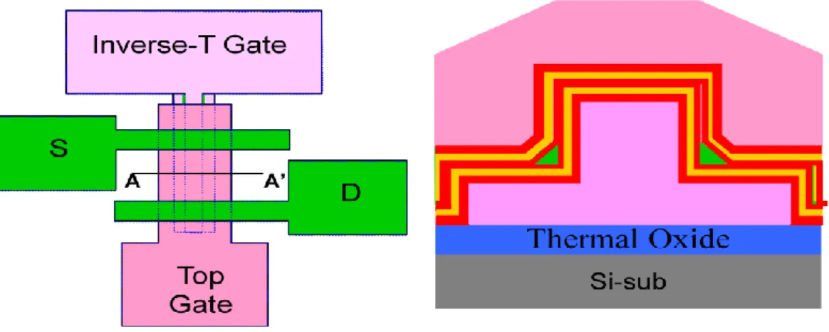
Fig2-1 Top view and cross-sectional view of the inverse-T double-gate NW-SONOS device.
36
Fig. 2-2(b) After removal of 100nm-thick n+-doped poly-Si in all regions except the central height of IVTG.
Fig. 2-2(c) After removal of the remaining 50nm-thick in-situ doped n+ poly-Si in all regions except the IVTG, leaving the final IVTG.
37
38
Fig. 2-2(e) Source/drain ion implantation.
39
40
Fig. 2-3 Dependence of the threshold voltage on channel length and drain bias. [2-17]
Fig. 2-4 Illustration of channel hot electron injection (CHEI) showing that under large drain bias, some channel electrons could become hot enough to surmount the Si/oxide barrier.
41
Fig. 2-5(a) Illustration of F-N tunneling occurring when Votis larger than υb.
Fig. 2-5(b) Illustration of direct tunneling occurring when X∅𝑏
ot> |Eot |>
∅b−∅n
xot ,
where Eot is the electric field across the tunneling oxide.