國立交通大學
國立交通大學
國立交通大學
國立交通大學
顯示科技研究所
顯示科技研究所
顯示科技研究所
顯示科技研究所
碩士論文
碩士論文
碩士論文
碩士論文
高效率與高演色性白光
高效率與高演色性白光
高效率與高演色性白光
高效率與高演色性白光
有機發光二極體
有機發光二極體
有機發光二極體
有機發光二極體之研究
之研究
之研究
之研究
A Comparative Study of high power efficiency and
color rendering index White Organic Light
Emitting Diodes
研
研
研
研
究
究
究
究
生
生
生
生:
:
:
:張
張
張
張
繼
繼
繼
繼
聖
聖
聖
聖
指導老師
指導老師
指導老師
指導老師:
:
:陳
:
陳
陳
陳
金
金
金
金
鑫
鑫
鑫
鑫
教授
教授
教授
教授
劉
劉
劉
劉
柏
柏
柏
柏
村
村
村
村
教授
教授
教授
教授
中華民國九十七年七月 中華民國九十七年七月中華民國九十七年七月 中華民國九十七年七月
國立交通大學
國立交通大學
國立交通大學
國立交通大學
顯示科技研究所
顯示科技研究所
顯示科技研究所
顯示科技研究所
碩士論文
碩士論文
碩士論文
碩士論文
高效率與高演色性白光
高效率與高演色性白光
高效率與高演色性白光
高效率與高演色性白光
有機發光二極體
有機發光二極體
有機發光二極體
有機發光二極體之研究
之研究
之研究
之研究
A Comparative Study of high power efficiency and
color rendering index White Organic Light
Emitting Diodes
研
研
研
研
究
究
究
究
生
生
生
生:
:
:
:張
張
張
張
繼
繼
繼
繼
聖
聖
聖
聖
指導老師
指導老師
指導老師
指導老師:
:
:陳
:
陳
陳
陳
金
金
金
金
鑫
鑫
鑫
鑫
教授
教授
教授
教授
劉
劉
劉
劉
柏
柏
柏
柏
村
村
村
村
教授
教授
教授
教授
中華民國九十七年七月 中華民國九十七年七月中華民國九十七年七月 中華民國九十七年七月
高效率與高演色性白光有機發光二極體之研究
A Comparative Study of high power efficiency and color
rendering index White Organic Light Emitting Diodes
研 究 生:張 繼 聖 Student: James Chang
指導老師:陳 金 鑫 教授 Advisor: Dr. Chin Hsin Chen
劉 柏 村 教授 Dr. Po Tsun Liu
國立交通大學
顯示科技研究所
碩士論文
A Thesis
submitted to Department of Photonics
College of Electrical Engineering and Computer Science National Chiao Tung University
in partial Fulfillment of the Requirements for the Degree of Master of Science in Display Institute
July 2008 Hsinchu, Taiwan, Rupublic of China
中華民國九十七年七月 中華民國九十七年七月中華民國九十七年七月 中華民國九十七年七月
高效率與高演色性白光有機發光二極體之研究
研 究 生:張 繼 聖
指導老師:陳 金 鑫 教授
劉 柏 村 教授
國立交通大學顯示科技研究所
摘 要在顯示器或照明之應用上,Organic light-emitting diode面板 是一個相當具有前景的新興科技。本研究首先製作四波段的螢光白光 元件,除了原本的三原色,另外加了黃光的成分,以期能夠更加提高 人眼的敏感性。雖然演色性可以達到87,然而過低的效率可能不足以 應用在照明之上。故另搭配磷光材料提升效率,並同時又保有足夠的 演色性,實驗結果發現以螢光藍搭配磷光紅、綠材料可以得到高達 13.5cd/A的效率,同時也擁有超過80的演色性,足夠用於一般的照明 應用之上。本研究另以螢光增感劑置放於元件結構之內,並利用磷光 綠光與螢光紅光之間的不完全轉移,得到高達16.7cd/A的效率。最 後,我以單色藍光OLED 搭配一外部色轉換層(External color tuning
layer)以形成白光OLED 元件。此種方式提供了一簡化的方法以形成 白光OLED 元件,也是目前製作白光LED的最主要方法。本研究發現以 螢光藍光搭配色反轉材料可以達到白光原點的光色。另外搭配使用藍 光磷光材料之非漸層式以及漸層式(Graded)的元件,研究結果發現漸 層式的元件具有最好的效率,磷光藍光FIrpic一單色光元件利用獨特 的漸層式做法,可以提升40%的效率。
A Comparative Study of high power efficiency and color
rendering index White Organic Light Emitting Diodes
Student: James Chang
Advisor: Dr. Chin Hsin Chen
Dr. Po Tsun Liu
Display Institute
National Chiao Tung University
ABSTRACT
OLED panels might become a booming future for next generation displays or solid state lighting. This study fabricated a highly efficient and improved color rendering index white OLED device with a “tetra-chromatic” emission system. The device achieved a CRI of 87, and is tuneable from the twilight to daylight sky color. However, due to the low efficiencies, phosphorescent based device structures were hence developed. A fluorescent blue plus phosphorescent green and red emission layer device is demonstrated to have an efficiency of 13.5 cd/A and color rendering index over 80, which is acceptable for illumination. We also adopted a phosphorescent sensitizer to excite a fluorescent dye
through resonant energy transfer by replacing the phosphorescent red material Ir(piq)3 into a fluorescent red material DCJTB. By using this
mechanism and by inefficient transfer from the green to red, a higher efficiency of 16.7 cd/A was reached due to the higher eye sensitivity of the orange-reddish emission color of DCJTB. Finally, an external color tuning layer to simplify the fabrication process of white devices by using a blue device plus yellow down conversion layer, which is a common technology in LED industry was developed. By the concept of complementary colors, these two colors produced white emission. In this part, we also studied the effect of graded devices, and found that a graded phosphorescent blue device provided a higher efficiency.
誌 謝 兩年的碩士生涯即將結束,在這一段時間裏頭,經歷了不少挫 折,當然也使我學到許多東西,得到許多寶貴的人生經驗。因為有了 身邊許多人的支持與鼓勵,使我能夠順利的完成這本論文。 首先我要感謝的是我的指導教授陳金鑫教授以及劉柏村教授,老 師們的專業智識領域都相當充足,使我能夠充分的吸收知識。除此之 外,每次報告實驗進度時老師都會細心的指導我,使我可以修正不足 以及沒有考慮周延的地方。除此之外老師也不厭其煩的幫我們修改投 稿文章,使我的實驗脈絡能夠更加清晰,文法以及章節排序也能夠更 加嚴謹。另外也因為老師允與我機會擔任長達一年的課程助教,使我 可以由中學習許多:諸如課程的安排,試卷的準備…,並且藉此一機 會使得我可以認識更多的同學。同時也謝謝口試委員謝宗雍教授、陳 登銘教授、李柏璁教授、陳皇銘教授對我的論文的指導與修改,使我 的論文更加趨於完整。 在實驗室我要特別感謝孟寰與一德學長對於我的研究上給予了 許多幫助與指導,使我逐漸熟悉製程的環境與實驗的設計,透過和學 長們的討論才能使這本論文更加完整。也感謝實驗室助理美貞的幫忙 與照顧。另外也感謝學長姐建名、博宇、宛芳、秀娟、超榮、圃成在
我遇到困難時都能提供援助。也謝謝學弟冠亨、長晏、尚裕、立峰、 維哲、翌霖、智昱的幫忙與鼓勵。 另外我也要特別謝謝大島優子、小野惠令奈等 AKB48 成員以及岩 田さゆり、大後寿々花、大塚愛、川嶋あい、久住小春、原田亞希、 等人對我的友情陪伴,讓我有勇氣與信心去面對挑戰。這兩年要感謝 的人太多了,無法一一描述,但我由衷感謝所有跟我結緣的朋友。 最後我將這份碩士學位的榮耀獻給我的父母親,因為你們的支持 是我不斷前進的動力,希望未來能更加努力,將所學回饋給社會。
Contents
摘 要………i ABSTRACT………..iii 誌 謝……….,v Contents………vii Figures Captions………ix Table Captions……….xiii Chapter 1 Introduction………1 1.1 Background………...11.2 History of the development of OLEDs……….6
1.3 Basic Concepts of OLEDs………....7
1.4 Motivation………...11
Chapter 2White OLEDs……….12
2.1 The Evolution of Lighting Sources………..12
2.2 Basic Characteristic for white lighting systems………...12
2.2.1 The CIE diagram……….13
2.2.2 Color temperature and correlated color temperature (CCT)………14
2.2.3 Color Rendering Index (CRI)/ color rendition index…..18
2.2.4 Eye Sensitivities and Efficiencies………20
2.3 Different methods for achieving white OLED………...21
2.3.1 Multi Emissive layer structure (MEML)……….21 2.3.2 Single Emission Layer Structure(Multiply doped emission
layer) ………..24
2.3.3 Color conversion method………26
2.3.4 Other methods for producing white light………28
Chapter 3 The materials and fabrication process………...34
3.1 Materials………...34
3.2 Fabrication Process………..36
3.3 The thermal evaporation system and other instruments……..37
Chapter 4 Results and discussion………..40
4.1 Fluorescent white OLED………..40
4.2 Phosphorescent white OLED………...47
4.3 Phosphorescent and fluorescent combined white OLED……52
4.4 OLED with an external color tuning layer………...61
4.5 Comparison of the white devices………..69
Chapter 5 Conclusions………...72
References………74
Biography………84
Figure Captions
Figure 1-1 Photographs of some OLED displays used in mobile phones..3
Figure 1-2 Photographs of Sony TV XEL-1(two pictures combined together)………3
Figure 1-3 Photographs of other OLED displays include Samsung U3, Panasonic SV-SD100, Sony EW-002 and Benq-Siemens S88 (model: Ohgo Suzuka)………..4
Figure 1-4 An OSRAM OLED Table lamp-- The OLED Lighting modules can rotate individually………5
Figure 1-5 A transparent OLED over a window in a roof would be able to allow natural light in during the day and provide fascinating illumination for the room at night………5
Figure 1-6 The mechanism of OLED panels--recombination of positive and negative charge carriers inside the organic layers must be perfectly arranged in order to yield visible light output………8
Figure 2-1 The CIE 1931……….……….13
Figure 2-2 The correlated color temperature (CCT)………15
Figure 2-3 The Stellar classification……….15
Figure 2-4 Stellar Spectral Types OBAFGKM………....16
Figure 2-5 Scorpius--Antares 3,500K………..16
Figure 2-6 Cygnus--Albireo 4,300K/12,100K………...17
Figure 2-7 The measuring method for CRI………...19
Figure 2-8 The 8 or extended CRI samples………...19
Figure 2-10 The eye sensitivities………..20
Figure 2-11 Multi-emission layer structure………..23
Figure 2-12 Single emission layer structure……….24
Figure 2-13 Proposed energy transfer mechanism in the white light device………26
Figure 2-14 The color conversion method………...27
Figure 2-15 Tandem structure………...28
Figure 2-16 A MPE structure………29
Figure 2-17 A WOLED using micro cavity………..32
Figure 2-18 A WOLED using UV light plus CCM method……….33
Figure 3-1 A drawn of the device picture……….37
Figure 3-2 The ULVAC thermal coater………38
Figure 4-1 The device structures (Set A)………..41
Figure 4-2 EL Spectrums of tri- and tetra-chromatic OLED devices under a luminance of 3000 nits (Inset) The current efficiencies of tri- & tetra- devices………...42
Figure 4-3 Viewing angle dependence of tetra-chromatic WOLED……43
Figure 4-4 2-D CIEx,y dependence of the devices………...44
Figure 4-5 3-D CIEx,y dependence with the luminance………..44
Figure 4-6 Spectral dependence with the luminance (Inset: the spectrum of twilight & daylight sky color)………45
Figure 4-7 (top) The %NTSC color gamut for device set A (bottom)The devices after color filter transmission(left: tri-chromatic, right: tetra-chromatic)………..47
Figure 4-8 A totally phosphorescent white OLED device (Set B)……...49 Figure 4-9 The HOMO and LUMO for each material in the device (Set
B)………..50 Figure 4-10 The efficiencies changes with the doping concentration of Ir(piq)3 (inset)The EL spectrum………...51 Figure 4-11 (left)The CIE 1931 positions of the devices(right) The
%NTSC color gamut………....52 Figure 4-12 Devices Structures (Set C)………52 Figure 4-13 EL spectrum and CIE positions………54 Figure 4-14 (top) The %NTSC color gamut for the devices (bottom)The devices after color filter transmission(left: phosphorescent, right: fluorescent plus phosphorescent)………55 Figure 4-15 The EL spectrum with different NPB thickness…………...56 Figure 4-16 Devices (Set D)……….58 Figure 4-17 (Set D) The EL spectrum with different DCJTB doping concentrations (left: normalized, right: un-normalized
intensity)………...59 Figure 4-18 The comparison of the five kinds of device structures in its power efficiency………...60 Figure 4-19 The concept of complementary wavelengths………61 Figure 4-20 The PL emission of the ECTL under different
concentration...62 Figure 4-21 The blue devices(Set E)………63 Figure 4-22 The efficiencies and EL spectra of device Set E…………..65 Figure 4-23 The device structures of device Set E after applying external color tuning layer (ECTL)………65 Figure 4-24 The efficiencies and EL spectra of device Set E after
Figure 4-25 The EL spectra of device Set E-C after conversion with 0.5 or 1.0wt.% ECTL………..68 Figure 4-26 The CIE 1931 positions and photograph of the devices…...71
Table Captions
Table 2-1 Some major efficiency of light systems………...13
Table 2-2 Multi-emission layers publications………..22
Table 2-3 Single emission layer publications………..24
Table 2-4 Phosphorescent sensitizer publications………26
Table 2-5 EL performance of the devices……….31
Table 4-1 EL performance of the devices (Set A)………46
Table 4-2 EL performance of the devices (Set B)………50
Table 4-3 EL performance of the devices (Set C)………56
Table 4-4 EL performance of the devices……….57
Table 4-5 EL performance of the devices (Set D)………60
Table 4-6 The EL performance of the devices before conversion(Set E).66 Table 4-7 The EL performance of the devices after conversion(Set E)…67 Table 4-8 Comparsion of the devices………...71
Chapter 1
Introduction
1.1 Background
New types of flat panel displays were developed during the past decades, such as the liquid crystal display (LCD), plasma panel display (PDP), field emission display (FED), organic electroluminescent display (organic light emitting diodes, OLEDs), etc. Among these, LCD displays has already been in mass production, and is one of the most popular display nowadays. OLEDs, which are self-luminous and do not require backlighting and module seems to be a good candidate for the next generation display.
Advantages of OLEDs over LCDs are: 1. High contrast & brightness over LCDs.
2. Fast response: The response time of OLEDs and LCD are about 10-6 and 10-3 second, respectively. This benefit might improve the blurring problem occurred in LCDs panels
3. Self emitting: No need the usage of backlight system, which significantly reducing the pigments needed to be used.
4. Thin film & robust design: OLEDs are tough enough to be used in portable devices such as cell phones and mp3 players.
5. Viewing angle: Can be viewed up to 170 degrees, OLEDs provide a clear and distinct image, even under direct sunlight.
7. High resolution: High information applications can be achieved by using an active-matrix (AM) OLEDs.
8. Flexibility: Can be produced on metal foil or plastic film.
9. Production advantages: Up to 20% to 50% cheaper than LCD processes since it doesn’t need module.
Nowadays, white organic light-emitting diodes (WOLEDs) had gained particular attention due to their promising applications in various solid-state lighting, including backlights in LCDs, automotive rear lights, airport runway lighting, and illumination light sources [1~5]. Full-color OLED displays incorporating WOLEDs with color filters are also a booming future for WOLEDs. OLEDs “installed” commercialized products are already seen in the market, and the audience all known how brilliant this technology could be. For displays, important commercialized products include:
(1) Mobile phones: Benq-Siemens S88 (2006), Samsung E428 main and sub-displays (2006), Nokia 7900 Prism (2007), Motorola U9
sub-display (2008) and Nokia 8800 Sapphire Arte (2008), etc.
Between these, Nokia 8800 Sapphire Arte even owns a 320 x 240 pixels, 2inch QVGA and 16,700,000 colors display [6].
(2) Mp3 players: A large amount of products utilize OLED panels as its display. For instance: Panasonic SV-SD100 (2005), Iriver S10 (2006), Iriver Clix (2007) and Samsung K5 (2006).
(3)Digital cameras: Kodak L658 (2005) and Samsung high end product NV24HD (2008).
Figure 1-1 Photographs of some OLED displays used in mobile phones (up) Nokia 7900 prism (bottom left) Nokia 8800 Sapphire
Arte (bottom right) Benq-Siemens S88
(4) TV panels: Sony XEL-1 (11-inch TV non-standard 960×540) (2007.12.1).
Figure 1-3 Photographs of other OLED displays include Samsung U3, Panasonic SV-SD100, Sony EW-002 and Benq-Siemens S88
(model: Ohgo Suzuka)
For solid state lighting:
No commercialized product is announced so far. However, PictivaTM OLED Displays from OSRAM Opto Semiconductors has a team of
around 50 research engineers working on the development of OLEDs in solid-state lighting. “In the future it will be possible to use OLEDs as flexible or transparent light sources. A transparent OLED over a window in a roof would be able to allow natural light in during the day and
provide fascinating illumination for the room at night”, said Dr. Bernhard Stapp, Head of Solid State Lighting at OSRAM Opto Semiconductors. [8]
Figure 1-4 An OSRAM OLED Table lamp-- The OLED Lighting modules can rotate individually [9]
A glance in the future:
Figure 1-5 A transparent OLED over a window in a roof would be able to allow natural light in during the day and provide fascinating illumination for the room at night [10]
We believe OLED products will be continuously brought in the market and will finally be accepted by the customers.
1.2 Historical development of OLEDs
OLED was invented in 1963, Pope et al. applied bias voltage on single crystal of anthracence and they observed EL (electro-luminance) from 10-20 nm thick crystal of anthracene at voltage above 400V. However, the operation voltage was too high for practical applications. Progress in device performance was achieved in 1965, when Helfrich and Schneider [11] yielded electron-hole injection by using electrolytic contacts based on Ce sulphate and Na sulphite. However, to obtain significant light output, these devices had to be driven at voltage as high as 100V and the power efficiency was relatively low. A further step towards feasible organic electro-luminescent devices was made in 1970s by the usage of thin organic films prepared by vacuum vapor deposition or the Langmuir-Blodgett technique instead of single crystals [12-14].
The development of organic multilayer structures considerably improved the efficiency of light-emission by achieving a better balance of the number of charge carriers of opposite sign and further lowered the operating voltage by reducing the mismatch of energy levels between the organic materials and the electrodes. In 1987, Eastman Kodak Company announced a bi-layer organic thin film device, with electron donor and electron acceptor, via vapor deposition process. They developed low-molecular-weight organic light emitting molecular sandwiched in between two electrodes and applied current to emit light. The performance of such device was improved tremendously, and this is the
rudiment model for present OLEDs. A multilayer OLED was introduced by Tang and Van Slyke at Eastman Kodak [15], and reported highly efficient OLEDs by using Alq3. This report inspired a great interest in
research and development of organic materials for optical and electronic devices. By using a hetero-layer structure of Alq3, each a few ten
nanometers (10-100nm) thick, sandwiched between indium tin oxide (ITO) and Mg:Ag alloy electrodes, they could achieve high power efficiency and acceptable lifetime at low operating voltage. Since then, OLEDs have become an active field of research because of its potential application in flat panel display. In 1990, Burroughes et al. in Cambridge [16] developed other kinds of OLEDs which were based on conjugated polymers, which we call them as PLEDs afterwards while the letter “P” stands for polymer. Spin coating is the major method for producing these kinds of devices. PLEDs overcomes OLEDs by using only one single emitting layer, which simplify the fabrication process over the later one; but the issue to find one single material which can satisfy all requirements is difficult. Hence, PLED still doesn’t seem to make its future. Moreover, OLEDs could also be fabricated on flexible substrates such as metal foil, plastic substrate ( PET, PEN, PES….), or even paper [17]. The low cost of materials and fabrication processes are promising factors for the continuing development of OLED.
1.3 Basic Concepts of OLEDs
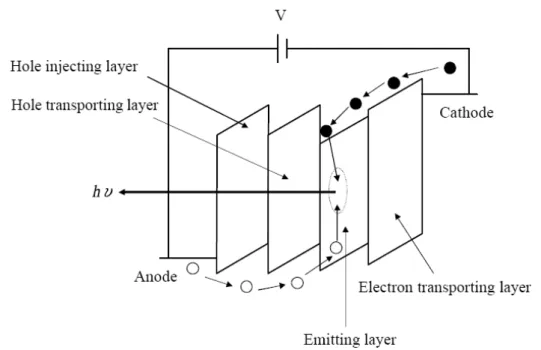
Positive and negative charge carriers (holes and electrons) need to transmit over organic layers and finally combine at the emission layer in order to produce the light emitting out of the OLED panel. The process
includes injection, transport, capture, and radiative recombination of the carriers. For simplicity, we will draw the spatial variation of the molecular energy levels in a band-like fashion; however, we have to bear in mind that these organic semiconductors are disordered materials without a well-defined band structure.
Figure 1-6 The mechanism of OLED panels--recombination of positive and negative charge carriers inside the organic layers must be
perfectly arranged in order to yield visible light output
The functions of each layer are explained as follows:
1. The anode:
High work function materials are preferred, for non transparent type (top emitting OLEDs), Au and Ag are the best selections, but Ag has a higher reflectivity. For bottom emission type OLEDs, the anode must be transparent for the light coupling side. ITO thus becomes the primary choice in this case. The work function of the ITO depends on its exact
stoichiometry (for ITO = 90% In2O3: 10%SnO2) and on the deposition
conditions, and it’s work function is approximately 4.7 eV; further increase of the ITO work function can be achieved by treating the surface with UV-ozone, oxygen or nitrogen plasma before depositing the organic layer to levels near 5.0 eV in order to match the hole injection layer barrier. Although techniques like plasma polymerization of the ITO have been suggested [18-20], further oxidation of the top surface using O2
plasma treatment is the most widely used method to increase the work function of ITO [21, 22].
2. The hole injection (p type) side (HIL):
The hole injection efficiency can be dramatic improved with this layer. The insertion of a thin conductive layer between the ITO and the emission layer has other advantages such as producing a smooth surface on which the ETL can be deposited (the ITO surface is too rough), and acts as a barrier for ions diffusion from the ITO into the emission layer, producing a large improvement in the device lifetime [23]. For PLEDs, PEDOT/PSS is often used as this layer.
3. The electron injection (n type) side (EIL):
For the cathode side, matching the organic lowest unoccupied molecular orbital (LUMO) level for electron injection requires the use of low work-function metals. The metals with the lowest work functions are the alkali metals [24]. However, their instability made them very difficult to evaporate in their simple metallic form. In this case, Ca and Mg are among the most widely used metals in OLEDs. A simpler and more
common way to reduce the Schottky barrier at the cathode-organic interface is to introduce a thin layer of fluoride, oxide or sulphide based on alkali or alkaline earth metals. Although LiF is the most commonly used material, other materials like CsF [25] and alkaline-earth fluorides [26] have also been successfully used. The efficiency of OLEDs can be improved by up to one order of magnitude when introducing a thin layer of fluoride between the emission layer and the cathode.
4. The emission layer (EL):
Well designed emission layers are very important for each OLED panel since the spectrum and efficiency of the device is largely determined by this layer. One single emission layer is used in the early day. Later, it was found that by using a dopant material, the efficiency, lifetime and satiability of the device can be improved. Tuning the emission color by using this method is also possible. For such cases, the primary conditions for such energy transfer are the amount of the overlap of the emission spectrum of the host and absorption of the guest. Therefore, the host material always needs higher energy gap than the dopant material. In the meantime, phosphorescent materials with their intrinsic high efficiency are introduced inside the emission layer, and the EQE(%) which stands for external quantum efficiency of the device is expected to reach 20%.
5. The cathode:
Al is the most commonly used material. For top emitting OLEDs, combined materials such as Al/Ag, Ca/Ag are often selected, with a total
thickness only about 20 nm. This is because Ag is more transparent than other materials.
1.4 Motivation
WOLEDs provide various applications for displays and solid state lighting products that can compete with conventional light technologies. My experiment focuses on producing WOLEDs devices with higher efficiencies and lighting ability OLED devices. Achieving this will require significant advances in efficiency, good CIE positions, and also acceptable CRI value.
So in order to achieve good performances, we focus on phosphorescent based device structures in order to improve the efficiencies while still remain acceptable CRI. In this thesis, several kinds of structures and devices are exanimated and the pros and cons between each kind of device structures, materials and also its effect on the CRI and %NTSC color gamut are compared.
Chapter 2
White OLEDs
2.1 The Evolution of Lighting Sources
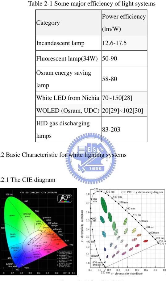
Lighting accounts for a large portion of the energy consumed each year, therefore the new, highly efficient sources of white light sources are urgently required. Today’s incandescent and fluorescent lamps have a limited efficacy of only around 4% (about 12 lm/W) and 25% (90 lm/W)
respectively. Conventional technology based on compound
semiconductors (i.e. LEDs) has made great progress in solving the problem and has now demonstrated efficacies of 70–100 lm/W. Nichia cooperation already demonstrated a prototype white LED with an power efficiency about 150 lm/W [28]; But, OLEDs also offer a very promising alternative, since it might reach flat, plain and large size uniform illumination. Also, the CRI value of OLEDs is higher than that of most nowadays illumination systems due to the large FWHM1 of each emitting material. Today’s state-of-the-art phosphorescent devices (PHOLEDs) from the Universal Display Corporation (UDC) are able to offer 60 lm/W at 1,000 nits. What’s more, it is anticipated that the efficiency of PHOLED technology will be able to break 100 lm/W by 2010 [27].
1
Table 2-1 Some major efficiency of light systems Category Power efficiency (lm/W) Incandescent lamp 12.6-17.5 Fluorescent lamp(34W) 50-90 Osram energy saving
lamp
58-80 White LED from Nichia 70~150[28] WOLED (Osram, UDC) 20[29]~102[30] HID gas discharging
lamps
83-203
2.2 Basic Characteristic for white lighting systems
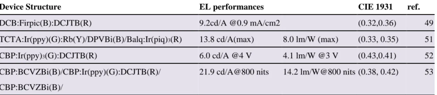
2.2.1 The CIE diagram
Figure 2-1 The CIE 1931
of the device. But this diagram has a major disadvantage, that is, the color difference is not average upon the figure. The green part of the diagram is much larger than the other half side of the picture. So we can hardly pick out the amount of color difference from this diagram.
2.2.2 Color temperature and correlated color temperature (CCT) 1. Definition:
The color temperature of a light source is determined by comparing its chromaticity with a theoretical, heated black-body radiator. The temperature at which the heated black-body radiator matches the color of the light source is that source's color temperature; for a black body source, it is directly related to Planck's law. However, most other light sources, such as fluorescent lamps and our OLED panels do not follow the form of a black-body spectrum (planckian locus), so in this case the correlated color temperature (CCT) is used. The CCT can be defined as the color temperature of a black body radiator which in the perception of the human eye most closely matches the light from the lamp. In Figure 2-2, we can estimate the nearly color temperature from the line projected out from the planckian locus, but for CIE positions that deviate this line too much, the CCT is meanless.
Figure 2-2 The correlated color temperature (CCT) [31] 2 . In the Space:
For the same case in the space, stars are also defined by its temperature and the color of light it emits. This is called the Stellar
classification. [32, 33]
Figure 2-4 Stellar Spectral Types OBAFGKM [33]
Figure 2-6 Cygnus--Albireo (4,300K/12,100K) [34-36]
Extremely high temperatures stars will show a bluish color with temperature over 30,000 K and is classified as O, only a small amount of stars lie in this category. Most of the stars are classified as A. Our neighborhood sun which is only 1 AU (149,597,870,691 + 30 meters) away emits a yellowish-white color having surface temperatures of about 5,778 K. But while the sun crosses the sky, it may appear to be red, orange, yellow or white depending on its position. The changing color of the sun over the course of the day is mainly a result of refraction and scattering of light, which is unrelated to black body radiation. Red giants (dying stars) have relatively low surface temperatures of about 3,600 K, but they also have a high luminosity due to their large exterior surface
area.
3. Solid state lighting:
Pulling the scope back to the solid state lighting, CCT only represent the feeling of the lighting source-- blue is the "hotter" color, while red is actually the "cooler" color. The colors of 5000K and 6500K black bodies are close to the colors of the standard illuminant called D65 (Daylight, T=6500K).
2.2.3 Color Rendering Index (CRI)/ color rendition index
In the calculation of the CRI, the color appearance of 8 reflective samples is simulated when illuminated by a reference source and the test source. The reference source is a Planckian radiator (if below 5000 K) or a CIE Daylight source (if at or above 5000 K), matched to the correlated color temperature (CCT) of the test source. After accounting for chromatic adaptation with a Von Kries correction, the difference in color appearance ∆Ei for each sample between the test and reference light
sources is computed in CIE 1964 W*U*V* uniform color space. The special color rendering index (Ri ) is calculated for each reflective sample
by:
Ri = 100 – 4.6△Ei
The general color rendering index (Ra ) is simply the average of
Ri for the first eight samples, all of which have low to moderate
A perfect score of 100 represents no color differences in any of the eight samples under the test and reference sources [31].
Figure 2-7 The measuring method for CRI
Figure 2-9 The reflectivity’s of the 8 color samples [31]
2.2.4 Eye Sensitivities and Efficiencies
The eye shows maximum sensitivity near 555 nm (for brightness over 3 nits), which shows a greenish-yellow color, but for brightness lower than 0.003 nits, the maximum sensitivity point shifts to 505 nm. So a light system composing of a green or yellow element might raise the efficiency due to the higher of the eye sensitivity with these colors.
2.3 Different methods for achieving white OLED
2.3.1 Multi Emissive layer structure (MEML)
White light emission can be obtained from multiple-emissive-layer (MEML) structures, in which different layers emit in different regions of the visible spectrum. Compared with other white OLED structures, such as the multi-doped emissive layer, the MEML is less complicated in fabrication process and more flexible in color tuning because not only doping concentration but also layer thickness can be used to modulate the device chromaticity. As a result, a merit of white OLEDs with a MEML is that its chromaticity can be tuned just by varying the thicknesses of the EMLs without changing the concentrations of phosphorescent dopants from their optimal values. Therefore, considering that the efficiency of doped OLEDs is sensitive to its concentration, white OLEDs with a MEML should have a higher efficiency than those with a multi-doped EML, in which at least one dopant is far away from its optimal concentration to achieve white emission. This is also the most common way to produce white light in the meantime—most of the reports use a bi- or tri- chromatic structures in order to produce white light. For a
bi-chromatic fluorescent WOLED, a yellow plus blue or magenta plus sky blue emitting layer is often seen. These structures demonstrated high efficiency (10-17 cd/A) and excellent stability at a reasonable voltage [38]. For the case of using phosphorescent materials, due to the lack of an efficient yellow emitting material, the multi emissive layer structure is often made into three layers composing of red, green and skyblue materials, but these kind of structure produces white color near the illumination point A [39]. The color is different from the white point, but might seem warmer for most illumination places. Some recent research is listed in the following table.
Table 2-2 Multi-emission layers publications
Device Structure EL performances CIE 1931 ref.
2002
CBP:FIrpic(6%)(B)/CBP:Btp2Ir(acac)(8%)(R) 11 cd/A(Max) 6.4 lm/W(Max) (0.37,0.40) @10 mA/cm2 40
2006
Ir(ppy)3(G)/Ir(ppq)2(acac)(R)/Firpic(B) 9.9 lm/W (0.44, 0.43)@1000nits 39
2007
mCP:Firpic(B)/CBP:Ir(piq)2(acac)R/mCP:Firpic(B) 10.8 cd/A EQE=7.6% (5000 nits) (0.33, 0.35) 41
[Firpic(B) /TL/(btp)2Ir(acac)(R)/ 17.2 cd/A@10834 nits (0.38, 0.42) 43
Ir(flpy)3(Y)/Ir(ppy)3(G)]
TCTA:PQIr(R)/mCP:Ir(ppy)3(G)/UGH2:FIr6(B) 32 lm/W EQE=16.6% (0.38, 0.39) 42
NPB(B)/Ir(Y):Ir(R):CBP/CBP/Ir(G):CBP 21.6cd/A 10.3 lm/W (0.39, 0.41) 44
CBP:Ir(ppy)3:Rb/CBP:Firpic/CBP:Ir(piq)2(acac) 27 cd/A EQE=12.4% (100 nits) (0.40, 0.42) 47
2008
4p-NPD:Ir(MDQ)2(Acac)/TPBI:Ir(ppy)3 31.6 lm/W EQE=15.2% (1000 nits) (0.49, 0.41) 45
So, in short we conclude some pros and cons of this structure:
The structure is more flexible in color tuning because not only the structure can be controlled by inserting blocking layers, but also each layers’ doping concentration and layer thickness. Some disadvantages include it needs relatively high operating voltage due to combined thicknesses of the many layers. Although BPhen, F4-TCNQ which are electron & hole injection layer materials (p-i-n device), may assist in reducing the voltage, but leads to deteriorate of the lifetime. In the meantime, some improvement trying to combine fluorescent and phosphorescent materials in order to produce white color is also introduced [46], because that the host material CBP or blocking layer BCP used in phosphorescent structures both have high HOMO values over 6.0 eV, leading to higher voltage issue. So, by using a blue fluorescent material, the voltage will drop and also reach a more saturated blue emission.
Di-chromatic Tri-Chromatic Figure 2-11 Multi-emission layer structure
2.3.2 Single Emission Layer Structure (Multiply doped emission layer) Single emission layer structure means that it’s emission layer is only composed of one layer. To ensure that all emission originates from a single thin layer, several dopants required to produce white light emission are mixed into a single host layer [48].
Table 2-3 Single emission layer publications
Device Structure EL performances CIE 1931 ref.
DCB:Firpic(B):DCJTB(R) 9.2cd/A @0.9 mA/cm2 (0.32, 0.36) 49
UGH4:Fir6(B):Ir(ppy)3(G):PQIr(R) 8.0 lm/W (0.43, 0.45) 48
Di-Chromatic Tri-Chromatic Figure 2-12 Single emission layer structure
Some other reports are based on using a phosphorescent sensitizer. This kind of device can be produced by either using single layer or multi layers device. The concept was first introduced by Stephen R. Forrest,
which produces yellow organic light-emitting devices by using DCM2 as a fluorescent lumophore, with a green electrophosphorescent sensitizer Ir(ppy)3. Exceptionally high performance for a fluorescent dye is due to
the ~100% efficient transfer of both singlet and triplet excited states in the doubly doped host to the fluorescent material using Ir(ppy)3 as a
sensitizing agent [50]. Then, Gangtie Lei et al. demonstrated a high-efficiency WOLED using a blue phosphorescent dye, which acts not only as phosphorescent sensitizer but also emitter. In this kind of WOLED, a fluorescent dye, DCJTB, and a phosphorescent dye, FIrpic, are co-doped into a new host material, DCB, to fabricate the emitting layer. White light emission can be obtained by the phosphorescent sensitized orange emission from the excitons in DCJTB molecules and the blue emission from those in FIrpic. The structure of white light device is ITO/NPB (50 nm) /DCB:FIrpic:DCJTB (91.6:8:0.4) (30 nm)/BPhen (40 nm) /Mg:Ag. A possible energy transfer mechanism of white light device is proposed in Figure 2-13. In FIrpic, the singlet excitons can transfer to the triplet states through the intersystem crossing process. As the EL spectrum of FIrpic partially overlaps the absorption spectrum of DCJTB, with the presence of DCJTB dopant, the triplet excitons in FIrpic can partially transfer to the singlet exciton in DCJTB through Förster transfer by dipole–dipole interaction. The DCJTB singlets then decay radiatively and give out light. The device with blue electrophosphorescent emission and phosphor-sensitized red emission exhibits a maximum current efficiency of 9.2 cd/A and maximum luminance of 18,200 cd/m2 were achieved [49]. Table 2-4 shows a few reports using the
phosphorescent sensitizer mechanism which also can be used in multi-emission layers devices; Table 2-3 shows some publications based on single emission layer.
Table 2-4 Phosphorescent sensitizer publications
Device Structure EL performances CIE 1931 ref.
DCB:Firpic(B):DCJTB(R) 9.2cd/A @0.9 mA/cm2 (0.32,0.36) 49
TCTA:Ir(ppy)(G):Rb(Y)/DPVBi(B)/Balq:Ir(piq)3(R) 13.8 cd/A(max) 8.0 lm/W (max) (0.33, 0.35) 51
CBP:Ir(ppy)3(G):DCJTB(R) 6.0 cd/A @4 V 4.1 lm/W @3 V (0.43,0.41) 52
CBP:BCVZBi(B)/CBP:Ir(ppy)(G):DCJTB(R)/ 21.9 cd/A@800 nits 14.2 lm/W@800 nits (0.38, 0.42) 53
CBP:BCVZBi(B)/
Figure 2-13 Proposed energy transfer mechanism in the white light device
2.3.3 Color conversion method
Blue emission layer with a down-conversion layer to produce white OLED is also developed. White light-emitting devices based on inorganic blue LED and down-conversion by phosphor were first published by Schlotter et al [54]. Duggal et al. were the first to implement the idea to
the field of OLED generating white light by combining a blue OLED with a down-conversion phosphor system [55]. However, the efficiency of this device is limited by the efficiency of the blue OLED. In 2006, the OSRAM Opto Semiconductors, Inc., fabricated a WOLED by using a down conversion system composed of YAG:Ce which has been widely used in most LEDs fabrication systems. This device produced an extraordinary enhancement on device performance, resulting in a white electroluminescence device with luminance efficacy of 25 lm/W and a luminance efficiency reaching 39 cd/A [56]. But this device only shows a CIEx,y of (0.26, 0.40), deviate from the E point on the black body locus.
Figure 2-14 The color conversion method
Figure 2-14 shows that the CIE points of the YAG:Ce particles, all the colors inside the yellow region can then be produced by altering the thickness of the composition of the phosphor particles.
2.3.4 Other methods for producing white light 1. Tandem/Stacked device
If we connect two units of OLED devices together by using charge generation layers, the efficiency of the OLED panel can significantly be improved by the offset of increasing the operation voltage. But while each layer only needs to emit 1/n of its original brightness, the lifetime of the OLED panel can obviously be improved. This concept was first produced by Professor Kido, and its structure is illustrated in the following figure:
Figure 2-15 Tandem structure [57]
There is a slightly difference in the meaning of tandem, stacked and multi photon structures. Tandem structure means the composition of many units of the same kind of structures, which cannot be operated seperately. A stacked structure means that each individual structure can be controlled seperately, so the preferable brightness of each layer can be controlled by giving it the current we want. And multi photon emission
(MPE) represents both kinds of structures. In 2007, Hitachi (ひたち,日立) company in Japan introduced a structure using fluorescent blue emission layer in the bottom unit (a mono-chromatic emission), and using phosphorescent green and red emission layers in the top unit (a bi-chromatic emission unit) in order to produce tri-chromatic white light, a charge generation layer is needed between the two units, this multi photon emission (MPE) structure is shown in the next figure: [58]
Figure 2-16 A MPE structure
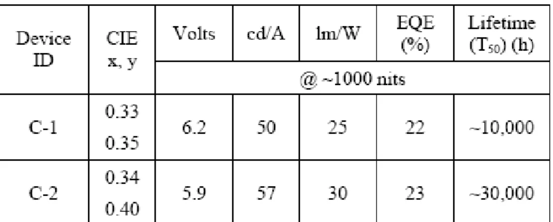
But the efficiencies of this device does not seems to reach its best performance. This “two-stack multi-photon emission structure” reaches a current efficiency of only 20.7cd/A, 4.6 lm/W, CIEx = 0.26, CIEy = 0.34, and 14.1 V at 1000 nits. Therefore, in SID 2008, Liang-Sheng Liao et al.
reported devices using the unique feature of the hybrid tandem white OLEDs combining both fluorescent blue emission and phosphorescent green and orange emissions. In order to investigate the effect of the blue color component on the overall EL performance of the whole device, two different fluorescent blue dopants, BDM1 and EK-BD9, were used to construct the two conventional devices. Device A-1 (BDM-1) has a preferred blue color for display applications. However, Device A-2 (EK-BD-9) has higher luminous efficiency and longer operational lifetime. It is therefore anticipated that the two blue EL units would contribute differently to white emission in a white tandem OLED. For the phosphorescent part of the device, in order to simplify layer structure and stabilize color gamut, they incorporated both a green and an orange emission into just one light-emitting layer. The orange emission dopant has a higher efficiency than the red one. Finally a tandem device is fabricated using organic intermediate connector because of its improved transparency and simpler fabrication process. The final performance table is shown in Table 2-5. Both devices provide extremely high current efficiencies over 50 cd/A, and good CIE performances [59].
Table 2-5 EL performance of the devices
2. Microcavity structure (MOLED):
By this way, only one emission layer is needed; this is also the hardest way to produce white light. For example, one device is shown
in Figure 2-17. This MOLED has a structure of
glass/DBR/ITO/NPB/Alq/MgAg. The Distributed Bragg reflector (DBR) and MgAg are the two mirrors to introduce the microcavity effect. The DBR consists of 2 ½ pairs of quarter-wavelength thickness Ta2O5 and SiO2 dielectric layers. DBR and ITO were deposited by
electron-beam evaporations. All organic and metal MgAg (10:1) layers were prepared by vacuum deposition. It basic structure is shown in Figure 2-17. White light was realized by controlling the microcavity structure, resulting in two cavity modes emission located at blue (488 nm) and red (612 nm) region. The layer thickness of each layer was produced by simulation. The bright EL emission has been obtained with a maximum luminance of 16435 nits, and maximum luminous efficiency of 11.1 cd/A. The CIE 1931 chromaticity coordinate of the
white color is (0.32, 0.34), which is very stable under different applied voltages [60].
Figure 2-17 A WOLED using micro cavity
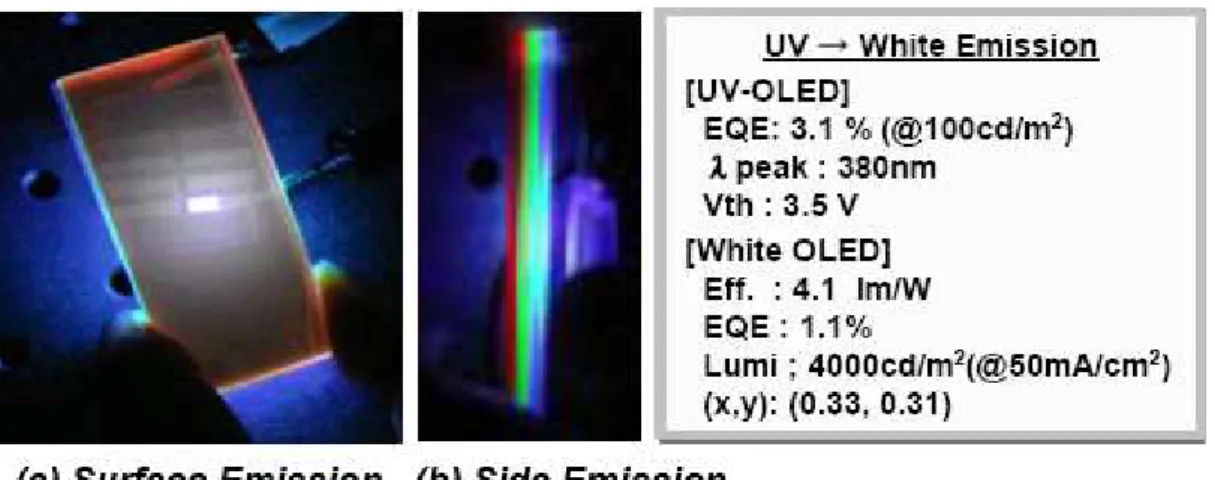
3. UV OLED +CCM layers
In 2008 SID, a new type of white OLED had been fabricated; this is also a technology being used in the LED industry. A basic concept and schematic structure of white emitting device by using “Color by UV” are shown in Figure 2-18. Red, green and blue three primary color conversion layers (CCL) were sequentially deposited on the glass substrate. In this case, UV light emission is firstly absorbed in the blue CCL and converted to the blue emission. Subsequently green CCL is efficiently excited by blue light emission and emits a green light. Similarly, red CCL absorbs the green light and shows a red emission. We can observe white light emission not only as a surface coupled emission from the front glass but also as a side coupled emission from the glass
edge. The emission intensity of UV-OLED is shown in Figure 2-18. The power efficiency reaches 4 lm/W under a luminance of 1000 nits, and 1.1% in EQE. Red and green emission intensities are slightly reduced in the side coupled emission because the intensity of waveguide mode changes with the refractive index as a function of emission wavelength. Color coordinates of surface and edge emission is (0.33, 0.31) and (0.31, 0.29), respectively [61].
Chapter 3
The materials and fabrication process
3.2 Fabrication process
Prior to the organic deposition, the ITO coated glass plate was patterned by lithography and then thoroughly cleaned by sonication, oxygen and CFx plasma treatment, in order to remove the micro particles and further increase the work function of the ITO glass to match the HOMO of the hole transport layer. All of the organic layers were then routinely deposited in a high vacuum chamber at the background pressure 5×10⁻⁴ Pa by thermal evaporation using resistively heated tantalum boats. Typically, the rate was controlled at 1.0 Å/s for obtaining smooth layer-layer interfaces. By careful control of the dopant boat temperature, it was possible to precisely co-evaporate a determined amount of dopant dispersed into the host emitter layer as measured in v/v%. After the deposition of the organic layers and without a vacuum break, the 1500 Å to 2000Å thickness of Al was deposited through a patterned shadow mask on top of the organic layers using separately controlled sources to complete the cathode prepare. Finally, the device is encapsulated in a glove box. The active area of the glowing size is defined as the overlap of the ITO and the cathode electrodes, which is 9 mm2. The EL emission spectra and current–voltage–luminance characteristics of the devices with encapsulation were measured in ambient immediately with a diode array rapid scan system using a Photo Research PR650 spectrophotometer and a computer-controlled direct current source. The operational stability of the devices was measured with encapsulation in nitrogen atmosphere to alleviate the influence of encapsulation condition. The LUMO, HOMO energy levels were measured using the atmospheric ultraviolet photoelectron analysis system (Riken AC-2) and the photoluminescence
spectra were obtained on the Acton Research Spectra Pro-150. The CRI, color temperature and the CIE (x, y) were measured by the JETI Spectro-radiometer 1210. These processes were performed right after the encapsulation of the device.
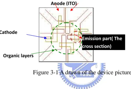
The experiment device:
The size of the glass substrate is 4cm×4cm. Each glowing pixel is fixed at 3 mm×3mm and one glass has a total of four individual pixels.
Figure 3-1 A drawn of the device picture
3.3 The thermal evaporation system and other instruments
Our thermal coater system is provided by ULVAC, and is showed in the following picture. It is composed of five chambers, each majorly for a specific usage.
Organic layers Cathode
Anode (ITO)
Emission part( The cross section)
Figure 3-2 The ULVAC thermal coater
Chamber 1 evaporates the hole/electrons transportation layers, chamber 2 evaporates the emission layers, and chamber 3 evaporates the metals and p- injection layer materials. Chamber 4 is for ITO sputtering and Chamber 5 is only a pre-treatment chamber.
Parts inside the chamber include:
(1) Holder: The samples are placed on top of it and when the main shutter & the small shutter are open, the materials can be evaporated to the sample.
(2) Crystal sensors: The deposited film thickness can be monitored by a gold crystal material, which has a frequency of 5MHz.
(3) Main/ Small Shutter: Each chamber has a main shutter and six small shutters.
(4) Crucible: Materials is injected inside the crucible, and when heated to the desired temperature, the deposition will come out.
Chapter 4
Results and discussion
4.1 Fluorescent white OLED
A tri-chromatic device composed of red, blue and green emission layers was fabricated. The device shows a yield of 8.3 cd/A, and an efficiency of 5.8 lm/W under a luminance of 1651 nits, and the CIE positions also lie in the white region. The addition of NPB layer between the red and blue emission layers is essential as it acts as an efficient hole transport material to increase hole concentration for recombination. If NPB was removed, the emission was almost totally red since the holes cannot penetrate further into the other emissive layers deeper inside the structure. For the electron transportation layer, BPhen is chosen other than Alq3 due to its higher electron mobility in order to balance the
charge-carriers for recombination. The electron and hole pairs will be confined inside the structure since a p-type/intrinsic/n-type junction is produced. Because of the higher eye sensitivity of our eyes in the green to yellow region near a wavelength of 555 nm, we then introduced a yellow layer tetra-chromatic white OLED device with four emission layers. This layer is added between the blue and green emission layers which match well with the green emission layer without creating another barrier. Our tetra-chromatic device has the following structure.
ITO/CFx/50% NPB:50% WO3 (200 Å)/NPB (100 Å)/60% Rb:40%
Å)/Alq:3%Rb (40 Å)/ Alq:1% C545T (100 Å) /BPhen (100Å)/ BPhen: 5% Cs2CO3 (200 Å)/Al (1500 Å).
Figure 4-1 The device structures (Set A)
As shown in Figure 4-2, our tetra-chromatic white OLED spectrum showed five peaks near 455, 479 (blue), 519 (green), 555 (yellow) and 608 (red) nm, with an overall FWHM well over 200 nm. Compared with the tri-chromatic spectrum, the nonuniform intensity among the R, G, B peaks are now alleviated with the additional yellow emission. While rubrene can trap charge carriers, further improvement of charge-carrier balance in holes and electrons is possible [62]. From the inset in Figure 4-2, a higher current efficiency is also obtained for the tetra-chromatic white OLED, the final CRI reaches 87. The value is still not very ideal due to the orange-reddish emitter DCJTB which is not saturated in red enough.
Figure 4-2 EL Spectrums of tri- and tetra-chromatic OLED devices under a luminance of 3000 nits. (Inset) The current efficiencies of
tri- & tetra- devices)
Figure 4-3 shows the viewing angle dependence of our device, which shows nearly the same intensity throughout a range of ±60 viewing angle. As this light source is not Lambertian, uniform illumination of the room is possible with our device due to very low angular dependency.
Figure 4-3 Viewing angle dependence of tetra-chromatic WOLED
Figure 4-4 and Figure 4-5 shows a specific advantage of the tetra-chromatic device in which a yellowish color is shown under low drive current density, with CIEx,y near (0.40, 0.44) can be readily obtained.
Similar color for the twilight sky is believed to be important in the regulation of the human circadian rhythm during the post-working duration [63]. Under high current densities for application of illumination in the daytime, a very near white point of CIEx,y (0.33, 0.36) can also be
achieved. These CIEx,y points appear to lie close to the locus points that
Figure 4-4 2-D CIEx,y dependence of the devices
From Figure 4-4, we can observe that the tetra-chromatic OLED differs from the tri-chromatic OLED in the colors. With a shift of about x=0.05 to the right side. Each of the three dots represents current densities of 0.5, 20 and 200 mA/cm2. By this way, the tetra-chromatic devices will also have CIE positions much closer to the white original point at (0.33, 0.33) under higher current density.
The spectral dependence with the luminance is shown in Figure 4-6, we can see that under lower luminance, the blue emission intensity is weaker, and gets stronger and stronger under higher brightness, thus leads to a more saturated white emission.
Figure 4-6 Spectral dependence with the luminance (Inset: the spectrum of twilight & daylight sky color)
From the efficiency Table 4-1, we can observe that the tetra-chromatic device contributes to the rise of yield from 8.3 to 8.7 cd/A, due to the higher sensitivity of yellow light to the human being’s eye, but while rubrene is a material that will extensively trap electrons [62], the voltage will also rises 0.6 V, so there is no improvement in the power efficiency. Both devices show white light emission with CIE positions of (0.30, 0.39) and (0.45, 0.40) under 20 mA/cm2 .
Table 4-1 EL performance of the devices (Set A)
Device Voltage (V) Current Efficiency (cd/A) Power Efficiency (lm/W)
EQE (%) CIE 1931 CRI %NTSC
color gamut
Tri- 4.5 8.3 5.8 3.7 (0.30, 0.39) 89 72.9
Figure 4-7 (top) The %NTSC color gamut for device set A (bottom)The devices after color filter transmission(left:
tri-chromatic, right: tetra-chromatic)
The color rendering indexes are very good with values of 87 and 89. Also good %NTSC color gamut was achieved with values near 70, the tetra-chromatic device have lower %NTSC value due to the insert of an yellow component, which shifts the green coordinate to the right, thus lead to the shrinkage of the %NTSC. Higher %NTSC values can also be reached by selecting a higher quality color filter. But fluorescent devices efficiencies are not enough for white solid state lighting, so we will next focus on using phosphorescent materials inside the OLED device for their capability for producing higher efficiencies. Our next part of research will emphasize on phosphorescent white OLED devices.
4.2 Phosphorescent white OLED
In the case of phosphorescent white OLED, tri-chromatic OLED devices were fabricated more often using the following materials—a green phosphorescent green material Ir(ppy)3. For the blueemission, we
uses a well known greenlish-blue dopant FIrpic. For red emission dopant, we uses Ir(piq)3, a well-known red phosphorescent dopant material which
emits pure red color with CIE coordinates of (0.67, 0.33). But unfortunately, Ir(piq)3 has a triplet bandgap of 2.0 eV and its HOMO and
LUMO are 5.2 eV and 3.2 eV, respectively, which is rather deep compared with other dopant materials. Although CBP with triplet bandgap of 2.6 eV is commonly used as a host for Ir(piq)3, the large
energy gap between CBP and Ir(piq)3 results in charge trapping in the red
dopant rather than energy transfer from CBP to Ir(piq)3 [64]. Therefore, a
triplet sensitizer which can induce efficient energy transfer from CBP to Ir(piq)3 is necessary to get high performances in Ir(piq)3 devices. Ir(ppy)3
has a triplet bandgap of 2.4 eV compared with 2.0 eV of Ir(piq)3 and it
may be suitable as a sensitizer for Ir(piq)3. In addition to energy bandgap,
there should be an overlap of emission spectrum of sensitizer and absorption spectrum of Ir(piq)3 to get high efficiency through efficient
energy transfer.
So for producing white light, we first exanimated a blue phosphorescent emission layer plus a red dopant Ir(piq)3 doped inside the
green emission layer Ir(ppy)3. The structure is shown in Figure 4-8, we
Figure 4-8 A totally phosphorescent white OLED device (Set B)
For the ease of the fabrication process, the whole multi-emission layer have the same host material CBP throughout, and is composed of an FIrpic doped CBP blue EML, an Ir(ppy)3 doped CBP green EML, and an
x % Ir(piq)3 co-doped inside the green emission layer. The CBP layer
close to NPB is to prevent the emission of NPB, and the layer between the two emission layers is to restrict the flow of the energy transfer from the blue emission layer to the other layers, which quenches the emission of FIrpic. And also a very thin layer hole blocking material BCP is added. By trapping the excitons, their residence time and recombination probability in the EML were increased, leading to a concomitant increase in OLED efficiency. A 30-nm-thick layer of Alq3 was used to transport
and inject electrons into the EML. Although the emission layers are all composed of phosphorescent materials, Ir(piq)3 while having a deep
triplet energy, which leads to high driving voltage at low doping concentration, is still not preferred. According to research data, the efficiency drops tremendously and the driving voltage rises heavily for
higher red doping concentrations, which means that more excitons trapped in this deep triplet level is not preferable.
Figure 4-9 The HOMO and LUMO for each material in the device (Set B)
Table 4-2 EL performance of the devices (Set B)
Device Voltage Yield(cd/A) Eff.(lm/W) EQE(%) CIE
1% 8.1 32.3 12.5 10.8 (0.27, 0.55)
1.5% 8.1 24.2 9.4 9.2 (0.29, 0.52)
2% 8.5 20.2 7.4 8.3 (0.32, 0.49)
According to Figure 4-10 and Chart 4-2, the efficiency drops from 32.3 cd/A for 1.0% concentration to 16.1 cd/A for 2.5% of Ir(piq)3, while
the voltage raises from 8.1 V to 9.4 V under 10 mA/cm2 current density. Hence, a doping concentration of at least 2.5% is needed to produce acceptable white emission. The color rendering index is fair with a value of 71.
Figure 4-10 The efficiencies changes with the doping concentration of Ir(piq)3 (inset) The EL spectrum
A disadvantage is that the emission of light deviates too much from the white point, which only has a CIE near (0.36, 0.48). This is because the FIrpic is not blue enough having a peak wavelength near 500 nm with CIE position near (0.18, 0.40). So, in order to solve this problem, one is to invent a more saturated blue phosphorescent material, and another is to use a blue fluorescent material with a deeper blue emission
and combine it with phosphorescent materials with other colors.
Figure 4-11 (left)The CIE 1931 positions of the devices (right)The %NTSC color gamut
Figure 4-12 Devices Structures (Set C)
4.3 Phosphorescent and fluorescent combined white OLED
Combining both fluorescent blue emission and phosphorescent green and red emission was then studied. We used the same structure as the totally phosphorescent device and only exchanged the FIrpic doped CBP host layer into a highly efficient sky blue fluorescent layer with MADN
dopant BUBD-1, we called these devices as Set C. The emission of this blue layer has a much bluer color rather than FIrpic which is an advantage in the fabrication of white OLED devices. The emission spectrum and CIE 1931 positions are shown in the Figure 4-13. For the white device, the fluorescent blue-emitting unit is formed close to the ITO anode side in each of the devices because the plasmon-quenching effect from the Al cathode on the blue emission could be avoided with this arrangement in order to obtain a maximal blue emission[65]. Again we evaluated the dopant concentration of Ir(piq)3 inside the Ir(ppy)3 layer,
for this layer nearly defines the total efficiencies and CIE positions. We tried 2.0% and 3.0%, and found that the one with a 3.0% shows a too strong red emission thus gives a purple device, and the current efficiency weakens to 7.3 cd/A. The best dopant concentration will be 2.0% in order to enter the white region. This is 0.5% lower than the totally phosphorescent device. This reason can be explained because the sky blue fluorescent dopant BUBD-1 has a deeper blue emission compared with FIrpic, which pulls the CIE positions with lower y coordinates, thus a lower red composition is needed. This is a good effect while the Ir(piq)3
![Figure 1-2 Sony TV XEL-1 [7]](https://thumb-ap.123doks.com/thumbv2/9libinfo/8761488.208297/19.892.160.722.418.1112/figure-sony-tv-xel.webp)
![Figure 1-4 An OSRAM OLED Table lamp-- The OLED Lighting modules can rotate individually [9]](https://thumb-ap.123doks.com/thumbv2/9libinfo/8761488.208297/21.892.146.746.108.538/figure-osram-oled-table-lighting-modules-rotate-individually.webp)