CF
4Plasma Treatment for Fabricating High-Performance
and Reliable Solid-Phase-Crystallized Poly-Si TFTs
Shen-De Wang,zWei-Hsiang Lo, and Tan-Fu Lei
Institute of Electronics, National Chiao Tung University, Hsin-Chu, Taiwan
A CF4plasma treatment on solid-phase-crystallized共SPC兲 poly-Si thin-film transistors 共TFTs兲 has been demonstrated. Using this technique, fluorine atoms can be introduced into the poly-Si film to passivate the defects, and hence, the device performance of the SPC poly-Si TFTs can be significantly improved. The fluorinated SPC poly-Si TFTs exhibit a good subthreshold slope, low threshold voltage, and high field effect mobility. Moreover, the fluorinated SPC poly-Si TFTs also exhibit an improved hot-carrier-stress immunity, which is due to the strong Si-F bonds formed in the poly-Si channel region.
© 2005 The Electrochemical Society. 关DOI: 10.1149/1.1955166兴 All rights reserved.
Manuscript submitted June 30, 2004; revised manuscript received April 1, 2005. Available electronically July 21, 2005.
Polycrystalline silicon thin-film transistors共Poly-Si TFTs兲 have attracted much attention due to the possibility to realize the integra-tion of switching pixels and their peripheral driver circuits on a single glass substrate of active matrix liquid crystal displays 共AMLCDs兲.1-3
Compared with conventional amorphous-Si TFTs, poly-Si TFTs have many advantages including higher driving cur-rent and greater carrier mobility. However, the trap states in the poly-Si grains and grain boundaries degrade the carrier’s transport and increase the off-stated leakage current.4-6To eliminate these trap states becomes the main topic for future production of high-performance poly-Si TFTs. Hydrogen-based plasma passivation is the most popular method utilized in the current production.7-9 Al-though hydrogenation can passivate the intragrain and grain bound-ary trap states in the poly-Si film, the hydrogenated poly-Si TFTs suffer from a serious reliability issue, which is attributed to the weak Si-H bonding. Recently, several studies have demonstrated the use of fluorine共F兲 atoms to fluorinate poly-Si films, which can improve performance and reliability of poly-Si TFTs, particularly under long-term electrical stress.10-15This is because fluorine atoms can termi-nate dangling bonds and replace weak bonds in the grain boundaries and SiO2/poly-Si interface, and thus reduce the trap states in the poly-Si channel. In addition, strong Si-F bonds, more stable than Si-H bonds, can greatly improve device reliability under long-term electrical stress.
Fluorine ion implantation共FII兲, the most adoptive fluorinating technique, has been investigated.10-13It is worth pointing out that the ion implantation method is no longer suitable for large-sized glass substrate application. Moreover, to activate the fluorine atoms and recover the defects created by FII, a subsequent high-temperature annealing is required. However, the high-high-temperature process is not compatible with current production. Kim et al. dem-onstrated the use of fluorinated oxide共SiOxFy兲 to replace FII, which
can serve as a diffusion source.14,15This technique increases manu-facturing processes because extra film deposition and etching pro-cesses are necessary. To date, although the effects of fluorination have been investigated and clarified, there is still a lack of a process-compatible technique to introduce fluorine atoms effectively into poly-Si films for the poly-Si TFT fabrication. In this work, we pro-posed a novel fluorinating technique by employing CF4 plasma treatment, which is a simple and efficient process. To avoid an un-wanted etching effect, we controlled the radio frequency共rf兲 to ap-ply a low power共5 W兲 to dissociate fluorine atoms, which were used to fluorinate the poly-Si film. The fluorinated poly-Si TFTs have been fabricated using this technique and their device characteristics and reliability have been investigated.
Experimental
The schematic diagram of the fabrication process is illustrated in Fig. 1. First, a 100-nm-thick amorphous silicon layer was deposited
on a thermally oxidized Si wafer by dissociation of SiH4gas in a low-pressure chemical vapor deposition共LPCVD兲 system at 550°C. Subsequently, solid phase crystallization 共SPC兲 was performed at 600°C for 24 h in N2ambient for the phase transformation from amorphous to polycrystalline silicon. Individual active regions were then patterned and defined. After standard RCA cleaning, samples were subjected to the CF4plasma treatment conducted in a plasma-enhanced chemical vapor deposition共PECVD兲 system at 350°C for 15 s, under a pressure of 200 mTorr and a power of 5 W. A 50-nm-thick tetraethyl orthosilicate共TEOS兲 oxide was deposited to serve as the gate insulator and a 200-nm-thick poly-Si film was deposited and patterned for the gate electrode. A self-aligned phosphorous ion implantation was preformed with the dosage and energy of 5 ⫻ 1015cm−2 and 40 keV, respectively. The dopant activation was performed at 600°C furnace annealing at N2ambient for 24 h, fol-lowed by a deposition of the passivation layer and a definition of contact holes. Finally, a 500-nm-thick Al electrode was deposited and patterned. The control samples were prepared without the flu-orinating process. To concentrate on revealing the fluorine passiva-tion effects of the CF4 plasma treatment, none of the additional hydrogenation process was performed on the control samples. The electrical and reliability characteristics were performed using an HP 4156B.
Results and Discussion
Figure 2 shows the transfer characteristics 共ID− VGS兲 for the control and fluorinated poly-Si TFTs. The measurements were per-formed at two different drain voltages of VDS= 0.1 and 5 V. The parameters of the devices, including the threshold voltage共Vth兲 and subthreshold swing共S.S.兲, maximum on-current 共Ion兲 and the mini-mum off-current共Ioff兲, were measured at VDS= 5 V. The threshold voltage was defined as the gate voltage required to achieve a nor-malized drain current of ID=共W/L兲 ⫻ 100 nA. The extracted de-vice parameters are listed in Table I.
Accordingly, the performance of the fluorinated poly-Si TFT is significantly improved. The threshold voltage and subthreshold swing of the fluorinated poly-Si TFT were found to be 8.3 and 1.73 V/dec, which are superior to that of the control one共12 and 2.06 V/dec, respectively兲. It is known that Vthand S.S. are strongly influenced by the deep trap states, associated with the dangling bonds, which have energy states near the middle of the silicon band-gap. Therefore, using CF4plasma treatment can effectively termi-nate the dangling bonds in the poly-Si and SiO2/poly-Si interface. In addition, the maximum on-current共Ion兲 and on/off current ratio of the fluorinated TFT are also better than that of the control TFT.
The minimum off-current 共Ioff兲 of the fluorinated device was nearly unsuppressed, which is consistent with the previous reports by Chern et al.11and Kim et al.15However, while the applied gate voltage was toward more negative共VGS⬍ −2 V兲, the fluorinated poly-Si TFT showed a smaller leakage current compared with that of the control TFT. As is well known, under a high electric field, the z
E-mail: [email protected]
Journal of The Electrochemical Society, 152共9兲 G703-G706 共2005兲
0013-4651/2005/152共9兲/G703/4/$7.00 © The Electrochemical Society, Inc. G703
) unless CC License in place (see abstract). ecsdl.org/site/terms_use
address. Redistribution subject to ECS terms of use (see 140.113.38.11
leakage current in the poly-Si TFT mainly comes from the trap-assisted band-to-band tunneling near the drain edge. This observa-tion suggests that there must be fewer trap states for the fluorinated poly-Si TFT, and thus the leakage current under a high electric field is reduced.
Figure 2 also shows field effect mobility vs the gate voltage of control and fluorinated poly-Si TFTs. The field effect mobility was calculated from the value of transconductance at VDS= 0.1 V. As is seen, the maximum field effect mobility of the fluorinated poly-Si TFT is higher than that of the control TFT. The fluorinated poly-Si TFT shows approximately 28% enhancement in the maximum field
effect mobility. Note that the field effect mobility is significantly affected by the tail states near the bandedge, which resulted from the strain bonds in poly-Si and SiO2/poly-Si interface.4 This feature implies that the CF4 plasma treatment cannot only terminate the dangling bonds, but also relieve the strain bonds. Based on these results, a schematic cross-sectional view of the SiO2/poly-Si inter-face is illustrated in Fig. 3. It is suggested that strong Si-F bonds replace the dangling and strain bonds for the fluorinated poly-Si films, and thus the performance of the device is greatly improved.
The grain boundary trap state densities共QT兲 of the conventional and fluorinated poly-Si TFTs were estimated by the Levison and Proano method.16,17 Figure 4 exhibits the ln关ID/共VGS− VFB兲兴 vs 1/共VGS− VFB兲2curves at low V
DSand high VGS. QTwas extracted from the slopes of these curves. Fluorinated poly-Si TFT exhibits a
QT of 1.32⫻ 1013cm−2, whereas the control TFT has 1.67 ⫻ 1013cm−2. This result implies that the CF
4plasma treatment can passivate the grain boundary trap states in the poly-Si film. To fur-ther study the fluorine passivation effect near the interface, the ef-fective interface trap states densities共Nt兲 near the SiO2/poly-Si in-terface were also calculated. From the S.S., by neglecting the depletion capacitance, Ntcan be expressed as18
Nt=关共S..S. /ln 10兲共q/kT兲 − 1兲共Cox/q兲 关1兴 where Coxis the capacitance of the gate oxide. The Ntvalues of the control TFT and the fluorinated TFT are 1.45 and 1.21 ⫻ 1013cm−2, respectively. The N
tvalues reflect trap states near the SiO2/poly-Si interface. Therefore, these results figure that trap states in both grain boundaries and the SiO2/poly-Si interface were re-duced by using CF4 plasma treatment, which results in great im-provement in device performance.
Figure 1. Schematic diagram of the poly-Si TFTs by using CF4 plasma treatment.
Figure 2. Transfer characteristics of the control and fluorinated poly-Si TFTs with VDS= 0.1 and 5 V.
Table I. Comparison of device characteristics of the control and fluorinated poly-Si TFTs.
Device parameters Conventional Fluorinated
Threshold voltage Vth共V兲 12 8.3
Subthreshold swing S.S.共V/dec兲 2.06 1.73
Maximum on-current Ion共A兲 180 279
Minimum off-current Ioff共pA兲 38.7 40.7
On/off current ratio Ion/Ioff共쐓106兲 4.65 6.85
Figure 3. Schematic cross-sectional view of SiO2/poly-Si interface with and without CF4plasma treatment.
G704 Journal of The Electrochemical Society, 152共9兲 G703-G706 共2005兲
G704
) unless CC License in place (see abstract). ecsdl.org/site/terms_use
address. Redistribution subject to ECS terms of use (see 140.113.38.11
Figure 5 shows the output characteristics共ID− VDS兲 of the flu-orinated and control poly-Si TFTs. As is seen, the driving current increases significantly for the fluorinated poly-Si TFT. This is due to the higher mobility and smaller threshold voltage of the fluorinated poly-Si TFT compared with the control TFT. The driving current increased 130, 84, and 55% at VDS= 20 V with VGS= 10, 15, and 25 V, respectively. Figure 6 shows the secondary ion mass spectros-copy共SIMS兲 profiles of the control and fluorinated poly-Si films. The SIMS profiles show that lots of fluorine atoms could be intro-duced into the poly-Si layer by using CF4plasma treatment, but not carbon atoms. The SIMS analysis also shows a notably high con-centration of fluorine atoms piling up near the SiO2/poly-Si inter-face, instead of in the deep poly-Si layer. These piled-up fluorine atoms can provide a more effective passivation of trap states, be-cause the quality of the SiO2/poly-Si interface is the main issue for carrier transport.
Figure 7 exhibits activation energy共Ea兲 vs gate voltage for the control and fluorinated poly-Si TFTs at VDS= 1 V. In the off-region 共low VGS兲, the value of Eareflects the required energy for carriers to leak by means of trap states, whereas in the on-region共high VGS兲, the value of Ea reflects the carrier transport barrier caused by the trap states within the poly-Si channel.19Compared with the control TFT, the extracted Eaof the fluorinated poly-Si TFT decreases in the on-region and increases in the off-region. That is to say, for fluori-nated poly-Si TFT, fluorine atoms can passivate the trap states and hence reduce the barrier height for the carrier’s transport when the device is turned on. Fewer trap states resulted in the increase of Ea in the off-region and thus, trap-assisted leakage current is sup-pressed after the fluorinating process. Moreover, in the subthreshold region, a steeper profile can be found for the fluorinated TFT, which proves that the interface quality of the fluorinated TFT was better than that of the control TFT.
Figure 4. ln关ID/共VGS− VFB兲兴 vs 1/共VGS− VFB兲2curves at V
DS= 0.1 V and high VGSfor control and fluorinated poly-Si TFTs.
Figure 5. Output characteristics of the control and fluorinated poly-Si TFTs with VGS= 10, 15, and 25 V.
Figure 6. SIMS analyses of the control and fluorinated poly-Si films.
Figure 7. Activation energy vs gate voltage of the control and fluorinated poly-Si TFTs.
G705
Journal of The Electrochemical Society, 152共9兲 G703-G706 共2005兲 G705
) unless CC License in place (see abstract). ecsdl.org/site/terms_use
address. Redistribution subject to ECS terms of use (see 140.113.38.11
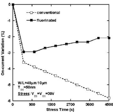
Additionally, the hot carrier stress was carried out to examine the reliability of the device. Figure 8 shows the variation of on-current under a hot carrier stress. The stress conditions were performed at
VDS= 30 V and VGS= 30 V for 4500 s. The variation of on-current was defined as 共Ion,stressed− Ion,initial兲/Ion,initial⫻ 100%, where the
Ion,initial and Ion,stressed are the measured Ion prior to and after the electrical stress. The on-current degradation can be attributed to two mechanisms: oxide trap charges and the creation of trap states in the poly-Si. They can be attributed to channel-hot-electron共CHE兲 and self-heating共SH兲 phenomenon. For CHE, electrons were injected and trapped in the gate oxide; then, the carrier flow is disturbed, reducing the ion. The SH-induced damage is due to the large Joule heat, resulting from a high drain current.20,21Because TFTs are fab-ricated on a poor thermal-conducting substrate, devices reach a very high temperature during operation. Such high temperature enhances bonds breaking to generate trap states in the poly-Si, and thus de-grades the TFT performance. As can be seen, the fluorination pro-cess can greatly alleviate the on-current degradation under a hot carrier stress. We deduce that by using CF4plasma treatment, due to the fluorine incorporation at the SiO2/poly-Si interface, the quality of the interface was greatly improved. The improved interface can result in great enhancement of gate oxide integrity.22Moreover, with Si-F bonds formed to replace weak bonds in the poly-Si, the bonds breaking can be eliminated. Hence, damage caused by CHE and SH
was suppressed for the fluorinated sample. As a result, device reli-ability was greatly improved for the fluorinated poly-Si TFT.
Conclusion
We reported a novel fluorinating technique of poly-Si TFTs by employing CF4plasma treatment. Using this technique, significant improvements in the performance of fluorinated poly-Si TFTs have been demonstrated. A steeper subthreshold slope, smaller threshold voltage, higher carrier mobility, and better on/off current ratio can be obtained due to the reduction of trap states in the poly-Si and the SiO2/poly-Si interface. Moreover, the CF4fluorinating process also improves hot-carrier immunity. It is concluded that the CF4 fluori-nation technique can provide a simple, effective, and process-compatible method to introduce fluorine atoms into poly-Si film to fabricate high-performance as well as high-reliability poly-Si TFTs.
Acknowledgment
The authors thank the National Science Council of the Republic of China, Taiwan, for financially supporting this research under con-tract no. NSC 93-2215-E-009-003 and NSC 93-2215-E-009-036.
National Chiao Tung University assisted in meeting the publication costs of this article.
References
1. I. W. Wu, Tech. Dig. AM-LCD, 1995, 7. 2. Y. Oano, J. Soc. Inf. Disp., 9, 169共2001兲. 3. J. Hanari, J. Soc. Inf. Disp., 10, 53共2002兲.
4. I. W. Wu, W. B. Jackson, T. Y. Huang, A. G. Lewis, and A. Ciang, IEEE Electron
Device Lett., 12, 181共1991兲.
5. G. K. Guist and T. W. Sigmon, IEEE Trans. Electron Devices, 45, 925共1998兲. 6. E. Korin, R. Reif, and B. Mikic, Thin Solid Films, 167, 101共1988兲.
7. C. F. Yeh, T. J. Chen, C. Liu, J. T. Gudmundsson, and M. A. Lieberman, IEEE
Electron Device Lett., 20, 223共1999兲.
8. H. C. Cheng, F. S. Wang, and C. Y. Huang, IEEE Trans. Electron Devices, 44, 64 共1997兲.
9. I. W. Wu, W. B. Jackson, T. Y. Huang, A. G. Lewis, and A. Ciang, IEEE Electron
Device Lett., 12, 181共1991兲.
10. S. Maegawa, T. Ipposhi, S. Maeda, H. Nishimura, T. Ichiki, M. Ashida, O. Tanina, Y. Inoue, T. Nishimura, and N. Tsubouchi, IEEE Trans. Electron Devices, 42, 1106 共1995兲.
11. H. N. Chen, C. L. Lee, and T. F. Lei, IEEE Trans. Electron Devices, 41, 698 共1994兲.
12. J. W. Park, B. T. Ahn, and K. Lee, Jpn. J. Appl. Phys., Part 1, 34, 1436共1995兲. 13. C. H. Fan and M. C. Chen, Electrochem. Solid-State Lett., 5, G75共2002兲. 14. C. H. Kim, J. H. Jeon, J. S. Yoo, K. C. Park, and M. K. Han, Jpn. J. Appl. Phys.,
Part 1, 67, 2247共1999兲.
15. C. H. Kim, S. H. Jung, J. S. Yoo, and M. K. Han, IEEE Electron Device Lett., 22, 396共2001兲.
16. J. Levinson, F. R. Shepherd, P. J. Scanlon, W. D. Westwood, G. Este, and M. Rider,
J. Appl. Phys., 53, 1193共1982兲.
17. R. E. Proano, R. S. Misage, and D. G. Ast, IEEE Trans. Electron Devices, 36, 1915共1989兲.
18. C. A. Dimitriadis, P. A. Coxon, L. Dozsa, L. Papadimitriou, and N. Economou,
IEEE Trans. Electron Devices, 39, 598共1992兲.
19. J. Y. Seto, J. Appl. Phys., 46, 5247共1975兲.
20. S. Inoue and H. Ohshima, Tech. Dig. - Int. Electron Devices Meet., 1996, 781. 21. M. Kimura, S. Inoue, T. Shimoda, S. W.-B. Tam, O. K. B. Lui, P. Migliorato, and
R. Nozawa, J. Appl. Phys., 91, 3855共2002兲.
22. Y. Mitani, H. Satake, Y. Nakasaki, and A. Toriumi, IEEE Trans. Electron Devices,
50, 2221共2003兲.
Figure 8. On-current variation as a function of stress time under a hot-carrier stress of the control and fluorinated poly-Si TFTs.
G706 Journal of The Electrochemical Society, 152共9兲 G703-G706 共2005兲
G706
) unless CC License in place (see abstract). ecsdl.org/site/terms_use
address. Redistribution subject to ECS terms of use (see 140.113.38.11