Characterization and Modeling of Out-diffusion of Cesium, Manganese
and Zinc Impurities from Deep Ultraviolet Photoresist
Fu-Hsiang Ko', Mei-Ya Wangb,
Tien-Ko
Wang', Chin-Cheng Yanga, Tiao-Yuan Huanga and
Cheng-San Wua
aNational Nano Device Laboratories, National Chiao Tung University, Hsinchu 300, Taiwan
b Department ofEngineering and System Science, National Tsing Hua University, Hsinchu 300,
Taiwan
ABSTRACT
The novel radioactive tracer technique was applied to investigate the migration of cesium, manganese and zinc impurities from deep ultraviolet photoresist into underlying substrate. Two important process parameters, viz., baking temperatures and substrate types (i.e., bare silicon, polysilicon, silicon oxide and silicon nitride), were evaluated. Our results indicated that the migration ratios were all below 6%, irrespective ofbaking temperatures and substrate types. The substrate types did not appear to strongly affect the metallic impurity out-diffusion from deep ultraviolet photoresist. However, solvent and/or
water evaporation due to temperature change was found to have a significant effect on metal migration. The net driving force of impurity changes with temperature and the impurity diffusion can be classified into four types. Based on the
proposed types, the obtained migration ratios can be realized. A new model, together with a new parameter, was proposed to describe the out-diffusion behavior of impurities from deep ultraviolet photoresist. The diffusion profile of photoresist was depicted based on diffusion equations and the migration ratios. This model could explain the migration ratios of metallic impurities in photoresist layers under various baking conditions.
Key words: DUV photoresist, impurity out-diffusion, radioactive tracer, impurity diffusion model
1. INTRODUCTION
The increasing complexity and miniaturization of modem integrated circuits demand a higher device yield and hence
lower defect density in the active region of silicon devices.' For a deep submicrometer device, a single metal precipitate
could cause a distortion of electrical properties and result in a faulty integrated circuit.25 For example, metals can degrade
the dielectric properties of gate oxide causing premature breakdown. They can also diffuse into the bulk of the silicon
substrate resulting in increased junction leakage as well as reduced minority carrier lifetime. Therefore, a better knowledge
of the diffusion route and behavior of the impurities introduced into the silicon substrate during device fabrication could
help to control the contamination and thus promote the circuit yield.
The control of fabrication processes involved in device manufacturing becomes more and more crucial due to increasing complexity for the materials and tools. Among them, lithography plays a very important role, because it is
applied repeatedly to the wafer surface during device manufacturing. Many lithographic models have been developed and applied for the photoresist profile simulation,68 however, the effects of impurity segregation and diffusion of Mn and Zn
impurities in the deep ultra-violet (DUV) photoresist have, to the best of our knowledge, not yet been reported. The behavior of metallic contaminants in DUV photoresist and their migration into the underlying substrate is of eminent
importance, because proper control of elemental impurity levels in the "high-purity" DUV photoresist would be very crucial for the fast proliferation of DUV photoresist in the IC industry in the coming years.9 Although it is always safer to demand an unnecessarily high degree of purity for DUV photoresist (i.e. 50-lOOppb for i-line and lO-3Oppb for DUV photoresist), however, the resulting cost would be extremely high and unnecessary. As this would require tedious sample pre-treatment procedures, including matrix decomposition by hot plate or microwave oven, separation, pre-concentration, and control of sample handling and analytical environment.'°'2 Therefore, a systematic study ofthe impurity diffI.ision behavior from DUV photoresist into the underlying substrate is technologically important and urgent, from the viewpoint of setting the proper
standard level oftolerable impurities in DUV photoresist for ULSI industrial application.
To evaluate the ratios of metallic impurities diffusing from DUV photoresist into the underlying substrate during
lithographic processing, e.g., baking, it requires various analytical methods for determining the impurities in the resist layer
and in the underlying substrate.'3 Methods that have been developed for detecting Cs, Mn and Zn impurities include
reflection X-ray fluorescence (TXRF) spectrometry, and secondary ion mass spectrometry (SIMS).
"'v
However, these methods suffer from the shortcomings"819 ofthe need to develop the decomposition method for the photoresist. They also require high sensitivity for the instrument, and are cumbersome in determining spectroscopic interference. In addition, the required blank control can seriously affect the analytical reliability during the measurement.202'Radioactive tracer technique2224 has proved to be very suitable for studying element migration in materials,
environment, and biochemistry. In semiconductor fabrication, the well-known RCA cleaning method,25 universally applied
in wafer processing for removing impurities from silicon wafer, was originally developed based on the radioactive tracer method by Kern and Puotinen in 1970. It is still in wide use today and forms the basis of many so-called "modified RCA
cleaning methods" for wafer cleaning. The effectiveness of the RCA cleaning method was first established by deliberately
contaminating the wafer surface with radioactive nuclides of Cu and '98Au. Gamma radioactivity was then recorded after and before RCA cleaning to monitor the cleaning efficiency. The advantages of the radioactive tracer technique are well
recognized; they include high throughput, easy operation, interference-free from stable isotope and reliability. Despite the versatility of the radioactive tracer technique, it has not yet been applied to study the impurity behavior during lithographic processes.
In this work, the radioactive tracer method was first introduced to investigate the migration ratio of Cs, Mn and
Zn impurities from DUV photoresist into the underlying substrate. The effects of various baking temperatures were evaluated. Furthermore, a diffusion model, together with a newly proposed parameter K, was suggested to describe the
impurity diffusion in the photoresist layer and its subsequent diffusion into the underlying substrate.
2. EXPERIMENTAL
2.1 Materials
P-type <100>wafersof 15cm in diameter were passivated with various films (i.e., polysilicon, silicon dioxide, silicon nitride). Non-passivated or bare silicon was used as a control. The wafers were cut into pieces, with 2cm by 2cm in area, to
serve as test samples. These test samples were prepared through various lithographic processes to study the behaviors of
contaminants introduced during the lithographic processes. Carrier-free radioactive tracers from DAMRI (France) were used in this study. The tracer composition was lOgIg of '37CsC1 (O.747M BqIg), 37tg/g of 54MnCl2 (0.838 M Bq/g) and lOtg/g
of65ZnCl2 (O.857M Bq/g) in 0. 1M hydrogen chloride solution.
The lithographic materials used in this work were DUV PR of SEPR-401H (Shin-Etsu Chemical, Japan). The
photoresist stripper was 1-methyl-2-pyrrolidone (NMP) obtained from E. Merck (Darmstadt, Germany).
2.2 Film Growing Process
To prepare different underlying surfaces for this study, films of polysilicon, silicon oxide, and silicon nitride were deposited onto various starting silicon wafers by low-pressure chemical-vapor-deposited (LPCVD) method in a quartz
reactor. The polysilicon film was deposited with silane gas (SiH4) at 60 sccm and 620'C .Thesilicon oxide layer was grown
by wet oxidation with a gas mixture of hydrogen (8 slm) and oxygen (4999 sccm) at 978°C .Thesilicon nitride film was deposited with a gas mixture of ammonium (130 sccm) and dichlorosilane (SiH2C12, 30 sccm) at 780°C.
Afterwards, wafers were cut into 2cm x 2cm pieces to serve as test samples, and a PR layer was then coated onto these
test samples. This procedure was accomplished by holding the test wafer by a vacuum chuck, and then dispensed lmL of
radioactive DUV PR onto the sample surface by a pipette. The coating processes of DUV PR were performed by spinning the samples at 1500 rpm for 0.5 mm. The PR samples were baked at 80, 100 and 120°C for 2 mm.
2.3 Radioactive Tracer Experimental Procedure
To prepare the radioactive DUV PR, one volume of diluted radioactive tracer (in O.005M HC1) was mixed with five volumes of lithographic materials. The radioactive lithographic solution was well-shaken to ensure homogeneous state, and was applied to the test samples by the spin-coating process mentioned above. After solvent evaporation, the test sample was
counted with an high resolution gamma-ray spectrometer. The counting system features an HPGe detector coupled with multi-channel analyzer (CANBERRA AccuSpec) and the usual electronics. The energy resolution of the system was
2.4KeV at 1332KeV. The intensity of gamma-ray for '37Cs (t11230. 15y), Mn (t1123 12.2 d) and 65Zn (t112=243.9d) was monitored at the energy levels of 661.7, 1115.5 and 834.8KeV, respectively. After counting, the PR layer was removed by
immersing in a lOOmL NMP solution at 60'C for 5 mm, followed by drying with a hot plate. The radioactivity of metal on
counting errors for lower radioactivity. The migration ratios of Cs, Mn and Zn from lithographic materials into the
underlying substrate were determined by the ratio ofthe time-average counts after and before film stripping.
3. RESULTS AND DISCUSSION
3.1 Metal Migration in DUV PR
Various possible behaviors, including diffusivity, solubility, precipitation and gettering, have been proposed
previously for the impurities existing in the silicon substrate during thermal treatment.227 However, little has been reported about the behavior ofmetallic impurities in DUV photoresist.
Since the photoresist layer after baking is an amorphous polymer, it is suitable to use the diffusion model for predicting the impurity behavior. Theoretically, the out-diffusion of impurity from photoresist should continue until equilibrium is reached. However, two features should be noted on describing the diffusion process. Firstly, the impurity diffusion coefficient in the photoresist is normally much higher than that in the underlying substrate. Secondly, the underlying substrate can act as a gettering-like region, therefore the impurity diffuses from the photoresist would mostly
appear in the upper region of substrate
nm27
In lithography, the soft-baking (usually on the hot plate), can remove most solvents. The solvent gradually evaporates away the photoresist layer, while metallic impurities in any chemical forms begin diffuse toward the substrate. Theoretically, the temperature-control diffusion can be simply described by the diffusion coefficient (D) and diffusion length (L):
D=D0exp—
(1)(2)
where D0 is the preexponential factor dependent on the vibration frequency of metallic impurity in the layer, and independent on the baking temperature. T is the diffusion temperature (in Kelvin), Q is related to the height of energy
barrier, k is the Boltzmann constant, and t is the diffusion time.
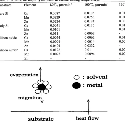
Table 1 summarizes the diffusion ratios of Cs, Mn and Zn impurities from DUV photoresist into various underlying substrates for three different baking temperatures (i.e., 80, 100, and 120°C). It can be seen that the (percentage) diffusion ratios are all below 6%, irrespective of the underlying substrates and baking temperatures. This shows that Cs, Mn and Zn
have low diffusion ability in the DUV photoresist at the normal baking temperatures used in this study. It is generally
anticipated that the diffusion may be promoted by elevating the reaction temperature. However, as can be seen from Table 1, the diffusion ratio does not show this dependency. The data for Cs decreases with the temperature for substrates of silicon nitride, while goes up for other substrates. The data for Zn decreases with temperature regardless of substrate, whereas Mn goes up then down for substrates ofbare Si and silicon nitride, and down then up for substrates ofpoly Si and silicon oxide. This tendency can be explained by the metallic ion migration mechanism proposed as follows.
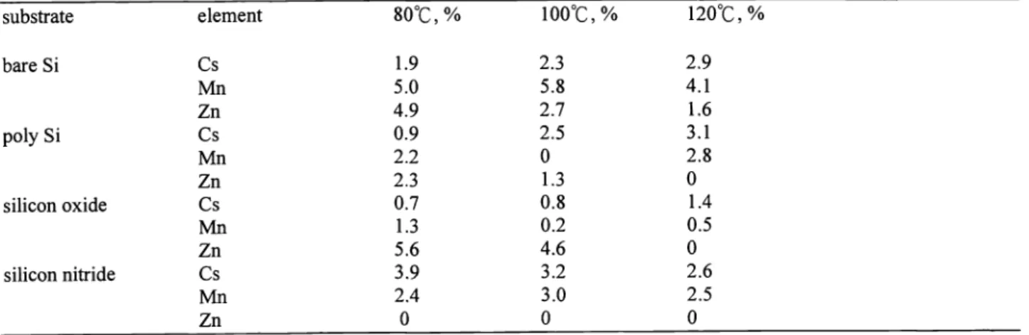
It is reasonable to consider that metallic ion can be solvated with the residual H20 or photoresist solvent to form M(H2O) or M(slovent) in the photoresist layer. As the film is heated, two pathways are possible as illustrated in Figure 1 . The baking temperature induces the metallic ion to move toward the substrate, while the solvated H20 or solvent
evaporates in the opposite direction. The net driving force of impurity changes with temperature and the impurity diffusion can be classified into four types as shown in Figure. 2. Type I describes the condition when the effect of impurity migration
dominates, while the effect of H20 or solvent evaporation is negligible; as a result, the diffusion ratio increases as temperature goes up. Type II is H20 or solvent evaporation dominates, while the effect of impurity migration is not significant; therefore, the diffusion ratio decreases as temperature goes up. Type III has a turnover temperature T. In the
temperature region when T<T1, the impurity migration is dominating and the net diffusion behaves like type I; whereas, when T>T, it behaves like type II. Type IV shows the opposite tendency as compared with type III.
Based on the proposed model shown in Figure 2, the experimental data appeared in Table 1 can be realized. The tendency of Cs diffusion for silicon nitride substrate can be attributed to type II; while for other substrates, they can be
attributed to type I. The tendency of Mn diffusion for substrates of bare Si and silicon nitride can be attributed to type III, whereas for substrates of poly Si and silicon oxide, it belongs to type IV. It is interesting to find that Zn has type II diffusion regardless of the substrate type. The diffusion ratio for Zn in silicon nitride substrate is near null, which is a special case of type II. This indicates that H20 and solvent evaporation can effectively restrict the Zn impurity from reaching the substrate.
3.2 The Temperature Effect on Metal Migration
diffusion length. Therefore without the consideration of other factor, the migration ratios should increase with temperature.
Interestingly, the migration ratios appeared in Table 1 did not follow this prediction as baking temperature was elevated from 80 to 120°C . The observation indicates the Equation 1 needs to be improved. In order to avoid the discrepancy, the
unknown function, f(T, t), is used to modify Equation 1
D =
f(T,t)D
exp
(3)where f(T, t) is dependent on heating type (e.g., hot plate, infrared-red or oven method), heating time, solvent evaporation, and structure of metallic impurity (e.g., free ion, hydration species or complex) and photoresist layer.
The differentiation ofmigration coefficient (in Equation 3) with temperature can be expressed by the following
ÔD
-Qaf
—Q Q
1f Q
—
= D
(exp—)(—) + JD (exp—)(---) =
D(——
+ —) .
(4)aT
0kT
T
°kT
2f
2Taking the layer density into consideration, the photoresist layer would become dense as elevating the baking
temperature. The higher baking temperature also induces higher evaporation rate of coexisting solvent, therefore the drag
force of solvent evaporation on migration of metallic impurities would become large. The metal impurity migrated across
the photoresist layer will face hindrance, especially at higher temperature, hence the term — < 0 .
The viewpoint13f
Qindicates
the unknown function —— term in Equation 4 is negative, while the other term — is positive regardless
faT
kT2
of the baking temperatures and substrate types. Here, the change of migration ratios with temperature can be classified into
1f
Qfour types, as shown in Figure 2. Type I describes the condition when the —— < —i- ,themigration ratio increases
fT kT
laf
Qas
temperature goes up. Type II appears at —— > —i- ,
themigration ratios decrease as temperature goes up. Typeiaj
QIII
has the turnover temperature (T) appeared at —— =
—i-
. In the temperature region when T<T1, the tendency of migration ratio behaves like Type I; whereas, when T>T, it behaves like Type II. Type IV also has the turnover temperature,but it shows the opposite tendency as compared with Type III. 3.3 Diffusion Model
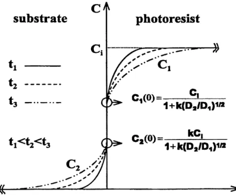
A semi-empirical diffusion model for the migration of metallic impurities from DUV photoresist into the silicon
substrate is described in Figure 3 . The initial concentration of metallic impurity in the photoresist layer is assumed to be C
at various cross sections. Equations 5and6, which describe the relationship for the impurity in the photoresist and the
(5)
at
oc
t32C—--=D
2(6)
ôt
Lunderlyingsubstrate at time t and location x, can be expressed as followings:
where C1 and C2 denote the concentrations of metallic impurity in the photoresist layer and the underlying substrate, respectively, D1 and D2 are the diffusion coefficients for the metallic impurity in the photoresist and the substrate,
respectively.
Two conditions are assumed for the above diffusion equations. The initial condition (t=O) gives C1 =C1and C2 =0.
Afterwards, a divergent behavior in the boundary condition is expected as diffusion proceeds (t>0). By assuming there is no accumulation or adsorption of the diffusing impurity at the interface, the interface boundary condition gives at x=O:
ac
ac
D1—1=D2-—-
7
ax
ax
Asolution to meet the diffusion model can easily be obtained by combining the semi-infinite medium assumption and
the initial and boundary conditions.28 The solutions are:
1 1/2 ________
c1=
jl+IqD2/D)
erj
1+k(D2/D1)2
2J7
kc,
_____
c2=
erfc
(9)
1+k(D2/D1)"2
where kC2/C1 (at x0) is the impurity segregation coefficient at the interface, erf(z) is the error function, and
erfc(z)=1-erf(z). The semi-infinite medium assumption needs X0>4(D1t)"2; it is valid only at relatively short diffusion time (X0 is the
thickness for photoresist layer). This assumption of short impurity diffusion length can also be verified by the small
percentage of diffusion ratio of experimental result as appeared in Table 1. It should be noted that, as diffusion proceeds, the impurity concentration at the interface (xO) remains constant at the values
c
c(o)=
I 11+k(D/D)112
(10)
kc
(11)
C2(0)
=
1+k(D
ID)112
3.4 The Parameter KFigure 4 illustrates the relationship of concentration gradient and location obtained by the semi-empirical model for the impurity in the underlying substrate and the photoresist layer. The concentration at the interface is always fixed at C1(O) and C2(O) as described by Equations 10 and 1 1. In addition, this figure demonstrates the trend of impurity-concentration change as impurities diffuse from the photoresist layer, with initial concentration C,, into the underlying substrate.
It is difficult to investigate the concentration gradient (C or C2) for impurity in the photoresist or substrate by
experimental measurement. While the radioactive tracer method demonstrates in this work can easily obtain the diffusion ratio without systematic error. With this advantage, a proposed model is derived as follows.
The rate of impurity migration through the interface is depicted below:
ac
ac2
kG
J=—D-—- =—D2-——
1 ax X0
ax X-
I(12)
1+k(D21D1)"2 V
t
The total amount of impurity diffusing into substrate in time t can be obtained by integrating the above equation:
(13)
whereA denotes the total area which is coated with DUV photoresist, and Q(t) is the numbers of impurity in unit area. Since the total amount of impurity (QA) in the experiment is equal to CXA, the diffusion ratio of diffusant after the bake can be expressed in the following:
Q(t)A
2
k
Jii5
2J
14Q1A
1+
k(D2 ID1)
X0
-Jx0
with
K=
k
(15)1+k(D2 ID1)112
The parameter K is first proposed and defmed in the impurity diffusion model, which is dependent on substrate type,
impurity structure, photoresist behavior and temperature. In addition, the parameter is independent of the baking time and impurity concentration. To describe the effect of temperature on K, the following equation is considered:
K(T) =
-
k(T)
E2Do,2eB
(16)
Do2e KBT1+k(T)[
'
Elf(T)Do,ie -:
Ei17
D1=
f(T)(Do,iei)
where k(T) and f(T) are unknown funëtions, T is the temperature in Kelvin, D01 and D02 are the pre-exponential factor
dependent on the vibration frequency of atoms in the lattice or interstitial sites, E1 and E2 are the binding energies at such sites, and k13 is Boltzmann constant. The f(T) function used to modify the impurity diffusion coefficient in the photoresist may be influenced by the heating type, evaporation pathway for photoresist solvent and structure for photoresist layer.
The DoieT term in Equation 17 increases with increasing temperature. While f(T) might decrease with elevating
bakrng temperature, since the structure ofphotoresist layer would become more condense during bake. In addition, Figure 1 also shown the H20 or solvent evaporation may also cause f(T) to decrease with increasing temperature. Therefore, D1 does not have to increase with increasing temperature. This is supported by the experimental observations presented in Table 1
that the diffusion ratios for Cs, Mn and Zn impurities from DUV photoresist into the underlying substrate did not show
significant temperature dependency.
For the diffusion coefficient, the value reported in literatures is always focused on high temperature process(>600°C).
Due to the substantially smaller value and the restricted instrumental method, little is reported regarding the diffusion
coefficient at low temperature. Therefore, in this work, we propose the parameter K to describe and simplify the diffusion model.
From Equation 14, the parameter K can be rewritten as:
K=1x12x fi
(18)
Q1A
2 Vt
With this the equation one may estimate the value of K for various types of impurity diffusion based on the experimental
results (i.e.. Table 1). It should be noted that small K represents low impurity diffusion, while large K represents high impurity diffusion. The resulting K values based on the data listed in Table 1 are illustrated in Table 2. The change of
parameter K value with temperature might be relevant to the model proposed in Figure 1 .Furthermore,if we assume that the diffusion coefficient for the impurity in the photoresist is much larger than that in the solid silicon substrate (D1>>D2) at
the normal baking temperature near lOOt ,a simplified representation for the parameter K can also be obtained from
Equation 15:
K =
k
(19)
1+k(—-)
If
either k or D2 is found, the other parameter can also be predicted from Equation 19 with K value known. The value ofeither k or 1)2 can describe the out-diffusion ofmetallic ion from the photoresist.
4. CONCLUSIONS
The characterization and modeling of impurity out-diffusion have been established to describe the mobility of cesium,
manganese and zinc impurities from DUV photoresist for baking temperature ranging from 80 to 120t .Only limited
amount of metallic impurity in the interface can diffuse. The diffusion ratio does not show strong baking temperature
dependency. The diffusion behavior can be explained by the net driving force of impurity diffusion and solvent evaporation using the model proposed in this work.
The concentration level of metallic impurity in the photoresist and underlying substrate can be calculated with the
proposed diffusion model. The diffusion ratio can be expressed by a newly proposed parameter K. With the prior
assumption for the relationship of diffusion coefficients (D1>>D2), the proposed parameter K is proportional to the segregation coefficient and square root of impurity diffusion coefficient of the underlying substrate. This model also
ACKNOWLEDGMENTS
The authors would like to thank the National Science Council of Taiwan, R.O.C., for supporting this research through
contracts #NSC89-TPC-7-3 1 7-00 1 and NSC89-272 1-23 17-200.
REFERENCES
1. S. M. Sze, VLSI Technology, p. 623, McGraw-Hill, New York (1988).
2. C. Y. Chang and S. M. Sze, ULSI Technology, p. 680, McGraw-Hill, New York (1996). 3. P. J. Ward, .1 Electrochem. Soc., 129, 2573 (1982).
4. M. Miyazaki, M. Sano, S. Sumita and N. Fujino, Jpn. I Appi. Phys., 30(2B), L295 (1991).
5. A. L. P. Rotondaro, T. Q. Hurd, A. Kaniava, J. Vanhellemont, E. Simoen, M. M. Heyns and C. Claeys, I Electrochem. Soc.,143, 3014 (1996).
6. F. H. Dill, W. P. Hornberger, P. 5. Hauge and J. M. Shaw, IEEE Trans. Electron Devices, ED-22, 445 (1975). 7. D. J. Kim, W. G. Oldham and A. R. Neureuther, IEEE Trans. Electron Devices, ED-3 1, 1730 (1984).
8. C. A. Mack, I Electrochem. Soc., 134, 148 (1987).
9. The National Technology Roadmap for Semiconductors, p. 93, Semiconductor Industry Association (1997).
10. J. Schram, FreseniusJ Anal. Chem., 343,727 (1992).
1 1 .
L.
Fabry, S. Pahlke, L. Kotz and G. Toig, Fresenius I Anal. Chem., 349, 260 (1994).12. F-H. Ko and M.-H. Yang, .1 Anal. At. Spectrom., 1 1, 413 (1996).
13. J. S. Crighton, J. Carroll, B. Fairman, J. Haines and M. Hinds, I Anal. At. Spectrom., 1 1, R461 (1996). 14. G. R. Fuchs-Pohl, K. Solinska and H. Feig, Fresenius I Anal. Chem., 343, 71 1 (1992).
15. M. D. Argentine and R. M. Barnes, .1. Anal. At. Spectrom., 9, 1371 (1994). 16. M. B. Shabani, T. Yoshihiro and H. Abe, I Electrochem. Soc., 143, 2025 (1996). 17. M. G. Dowsett, R. D. Barlow and P. N. Allen, J. Vac. Sci. Technol., B12, 186 (1994). 18. E. H. Evans and J. J. Giglio, .1 Anal. At. Spectrom., 8, 1 (1993).
19. R. N. SahandP. H. Brown, Microchemicalf., 56, 285 (1997).
20. G. Tolg, Talanta, 21, 327 (1974). 21. J. W. Mitchell, Talanta, 29, 1035 (1982).
22. R. J. Borg and G. J. Dienes, An Introduction to Solid State Diffusion, p. 255, Academic Press, CA (1988). 23. I. P. Glekas, WaterSci. Technol., 32, 179 (1995).
24. G. R. Choppin and J. Rydberg, Nuclear Chemistry, p. 425, Pergamon Press, Oxford (1980). 25. W. Kern and D. A. Puotinen, RCA Rev. ,31 ,187 (1970).
26. K. Graff, Metal Impurities in Silicon-Device Fabrication, p. 7, Springer, Berlin (1995).
27. J.-P. Joly, Microelectron. Eng., 40, 285 (1998).
28. J. Crank, The Mathematics of Diffusion, p. 38, Oxford Uni. Press (1976).
Table 1. The diffusion ratio for impurities transported from DUV photoresist into underlying substrates at various baking temperatures. substrate element 80°C,% 100°C,% 120°C,% bare Si Cs 1.9 2.3 2.9 Mn 5.0 5.8 4.1 Zn 4.9 2.7 1.6 polySi Cs 0.9 2.5 3.1 Mn 2.2 0 2.8 Zn 2.3 1.3
0
silicon oxide Cs 0.7 0.8 1.4 Mn 1.3 0.2 0.5Zn
5.6 4.6 0 silicon nitride Cs 3.9 3.2 2.6Mn
2.4 3.0 2.5 Zn 0 0 0Table 2. K value for impurity diffusion at various baking temperatures.
Substrate Element 80°C, tmmin1
100°C, immin'
120°C, lxmmin1bare Si Cs 0.0087 0.0 105 0.0133 Mn 0.0229 0.0265 0.0188
Zn
0.0224 0.0124 0.0073polySi
Cs 0.0041 0.0115 0.0142Mn
0.0101 - 0.0133 Zn 0.011 0.0062 -siliconoxide Cs 0.0054 0.0062 0.0 108Mn
0.0094 0.0014 0.0036 Zn 0.0404 0.0332 -siliconnitride Cs 0.0122 0.01 0.0081 Mn 0.0075 0.0094 0.0078 Zn-
-
-evaporationl
0
: solvent
• metal
migratio
substrate
heat flow
Figure 1. The effect of photoresist baking on impurity migration.type 1
type II
L
temperature
temperature
type III
type IV
4
oo
temperature
temperature
Figure3. The diffusion model for the impurity migration from photoresist into substrate.