國 立 交 通 大 學
電子物理研究所
博 士 論 文
微結構鐵磁系統的磁矩翻轉和磁電傳輸性質
Magnetization Reversal and Magneto-transport in
Patterned Ferromagnetic Systems
研究生:鍾廷翊
指導教授:許世英
微結構鐵磁系統的磁矩翻轉和磁電傳輸性質
Magnetization Reversal and Magneto-transport in Patterned
Ferromagnetic Systems
學生:鍾廷翊
Student: Ting-Yi Chung指導教授:許世英博士
Advisor: Dr. Shih-Ying Hsu國立交通大學
電子物理研究所
博士論文
A Dissertation
Submitted to Department of Electrophysics
College of science
National Chiao Tung University
in Partial Fulfillment of the Requirements
for the Degree of
Doctor of Philosophy
in
Electrophysics
May 2009
Hsinchu, Taiwan, Republic of China
Magnetization Reversal and Magneto-transport in Patterned
Ferromagnetic Systems
Student: Ting-Yi Chung Advisor: Dr. Shih-Ying Hsu Department of Electrophysics
National Chiao Tung University Hsinchu 300, Taiwan
Abstract
We present the magnetization reversal and magneto-transport in patterned ferromagnetic systems where the dimensions and lateral shape of samples play significant roles.
In the investigation of micromagnetism, in-plane magnetoresistance (MR) and in-field magnetic force microscopy (MFM) on a series of permalloy (Py) planar wires were performed. Here, the wire length and thickness are kept constant, 20mm and 30nm, respectively. The width of the wire spans from 10 to 0.1mm. The magneto-transport behavior and magnetic configuration are quite different regarding their widths, corresponding to the aspect ratio. For wire of large width (w>2mm), remanent state is a multi-domain configuration, the magnetization reversal is via the well-known domain expansion and all behaviors are under expectation. We focus on the narrow wire with w<2mm to explore the micromagnetic configuration of the so called “single domain” wire in which the abrupt switch of magnetization reversal occurs. According to their behaviors, we catalog them into three regions. For wire with width less than 0.5mm, a typical single domain state with moment along the long axis is observed. The moment barely rotates and switches suddenly to the opposite direction when magnetic field reaches the switching field. The other two kinds of wire have clear domains in both ends at remanence. When wire width is between 1.2 and 2mm, both end domain regions expand to the whole volume of the wire with increasing magnetic field in the opposite direction. A 180o cross-tie like wall forms right before switching. When wire width is between 0.5 and 1.2mm, the expansion of end domains does not extend to the whole volume before switching resulting in a spatial dependent in-plane MR behavior. Moreover, angular dependence of the
switching field of wires less than 1.2mm can be described using Aharoni model under the consideration of curling for the ellipsoid. When a wire width less then 0.3mm, the condition for curling mode is no longer fulfilled, there are deviation at large angles. We find that the magnetization reversal for all narrower wires (w<1.2mm) originates from the same mechanism of local nucleation and the propagation of the domain wall.
In the study of the angular dependence of Néel wall resistance, we create the centipede-like Py structure which consists of a central wire with numerous orthogonally bisecting finger wires. All Py wires were designed to have a single domain structure at remanence and high anisotropy by the geometric control. The remanent domain at the junction between the central and finger wires is determined by the anisotropy constants of both wires and hence, variable angles of Néel wall can be achieved. Developing a simple resistance-in-series model in corporation with the anisotropic MR effect, the analyses of the longitudinal and transverse MRs of the centipede-like structure give the domain wall resistance. Our results show that the Néel wall resistance is about mΩ and decreases with decreasing the relative angle between two domains.
微結構鐵磁系統的磁矩翻轉和磁電傳輸性質
學生:鍾廷翊 指導教授:許世英博士
國立交通大學電子物理所
大綱
此篇論文探討在鐵磁微結構中的磁矩翻轉和磁電傳輸性質,樣品的尺度和形 狀在這些微結構中扮演著重要的角色。 在研究微磁學時,我們以平行膜面磁阻的量測和施加磁場下觀察磁區的磁力 顯微來從事一系列鎳鐵合金毫微米線的磁矩翻轉研究,這一系列毫微米線的線長 和厚度分別固定為 20 微米和 30 奈米,線寬則由 10 微米變化至 0.1 微米,線寬 的改變將造成磁電傳輸行為和磁區結構有截然不同的結果。當線寬大於 2 微米是 屬於多磁區結構,磁區翻轉是藉由已確知的磁區擴張來完成,而對應的磁相關行 為也是可預期的,此篇論文將針對線寬小於 2 微米屬於所謂單一磁區的毫微米線 研究其微磁結構,根據磁翻轉行為,單一磁區的毫微米線又可被區分為三種類 型,當線寬小於 0.5 微米,在未達到磁瞬間翻轉場前,磁矩幾乎都平躺於長軸, 只有在超過磁翻轉場後,磁矩才瞬間翻轉至反向,其餘的兩種類型,在零磁場時, 線的兩端都有漩渦封閉磁區結構,對於線寬介於 1.2 和 2 微米,位於線兩端的磁 區結構會隨著反向外加磁場的增加而擴及至樣品整體,在瞬間翻轉前會觀察到類 似於 180 度 cross-tie 的磁區壁結構,當線寬介於 0.5 和 1.2 微米,磁區擴張 則不會擴及至樣品整體,導致在樣品不同部位觀察的磁電阻行為有明顯的差異, 此外,當線寬小於 1.2 微米,瞬間翻轉磁場與磁場相對毫微米線角度的相互關係 可以被建構在 curling 翻轉方式的 Aharoni 模型描述,當線寬小於 0.3 微米,由於幾何形狀已經不完全符合 curling 翻轉方式的考量,使得大角度的數據和模 型有明顯的偏離,我們發現當線寬小於 1.2 微米時,磁矩翻轉都是透過局部的翻 轉搭配磁區壁的移動來完成。 以我們對毫微米線的了解也進一步的研究 Néel 磁區壁電阻,我們設計了一 系列類似蜈蚣的多腳樣品,包含了許多相互垂直的鎳鐵毫微米線,這些線都因幾 何形狀的選擇而有單一磁區結構和高異向性。如此一來,位於兩線交錯區的零磁 場下磁矩方向將決定於這兩線的異向性能比值,因此創造不同角度的 Néel 磁區 壁,利用簡單的電阻串聯模型配合異向性磁阻來分析磁場平行電流和磁場垂直電 流的磁阻結果,磁區壁電阻即可被估算出來。我們發現 Néel 磁區壁電阻大約是 毫歐姆且隨著磁區壁兩邊磁區的相對角度變小而變小。
致 謝
向上天祈求,
心智成熟
上天賜與我一次又一次的失敗試驗
向上天祈求,
思考周全
上天賜與我一次又一次的錯誤嘗試
向上天祈求,
心平氣和
上天賜與我六年的時間磨練
六年來
要感謝的人好多好多
只好謝天了
CONTENTS
List of Tables i
List of Figures iii
1 Introduction...1
2 Theoretical Background...5
2-1 Energy consideration of domain formation ...5
2-1-1 Fundamental magnetic energies ...7
2-1-2 Domain structure in wires ...12
2-2 Magnetization reversal in wires...17
2-2-1 Magnetization reversal by Uniform rotation...19
2-2-2 Nonuniform magnetization reversal...23
2-3 Magnetoresistance of ferromagnetic wires...25
2-3-1 Anisotropic magnetoresistance...26
2-3-2 Domain wall resistance ...28
3 Experimental Details...34
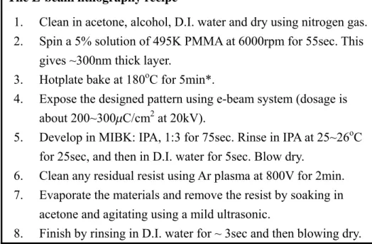
3-1 Device fabrication...34
3-1-1 Photolithography ...36
3-1-2 Electron beam lithography ...38
3-2 Measurement techniques ...40
3-2-1 Magnetoresistance measurement...40
3-2-2 Magnetic domain observation ...42
3-3 Characteristics of permalloy (Ni80Fe20) samples ...45
3-3-1 Magnetization hysteresis loop...46
3-3-2 Resistivity of permalloy wires...47
4 Experimental Results and Discussion...50
4-1 Remanent domain structure in individual wires ...50
4-1-1 Geometrical description ...51
4-1-2 Domain structure ...53
4-2 Magnetization reversal in individual wires ...55
4-2-1 Magnetoresistance and in field MFM images ...57
4-2-2 Analysis of Magnetoresistance...66
4-3 Domain wall resistance in the centipede-like structures ...85
4-3-1 Magnetoresistance...89
4-3-2 Planar Hall effect...93
4-3-3 Analysis of domain wall resistance ...95
5 Conclusions and Future work ...104
5-1 Summary...104
List of Tables
1 Qualitative comparison between different domain observation methods...43 2 Parameters of numerous samples………...82 3 Summary of other DWMR studies………....88
List of Figures
2-1 Domain structures related to the dimension………..………….…...6
2-2 Demagnetizing factors of a prolate ellipsoid……….11
2-3 Theoretical domain diagram of a prolate ellipsoid………...……….14
2-4 A formation of a flux closure pattern in a rectangle……….………..16
2-5 Theoretical expectation of the reversal mechanisms……….………...…...…...19
2-6 Energy diagram based on Stoner-Wohlfarth model………...22
2-7 Angular dependence of switching fields….………...24
2-8 Angular dependence of resistivities of AMR and PHE………...………...28
2-9 Numerical spin orientation in a domain wall...………..…………29
3-1 SEM images of a typical device ………...………35
3-2 SEM images of a typical photolithography pattern………... 37
3-3 Electron beam lithography patterns………...39
3-4 Force diagram of MFM……….……45
3-5 Magnetization hysteresis loops of permally samples……..………...47
3-6 Resistivity as a function of permalloy wire widths………48
4-1 The topography of our permalloy wires……….52
4-2 Remanent domain diagram of permally wires………...54
4-3 A SEM image of a typical permally wire device………58
4-4 Angular dependence of saturated sheet resistances ………...60
4-5 MR curves of a 10 mm wide wire………...61
4-6 LMR curves and MFM images for a 10 mm wide wire ……….63
4-7 MR curves of a 0.43mm wide wire……….64
4-8 MR curves measured at different parts of a 0.43mm wide wire……….65 ii
4-9 MR curves of a 1.9mm wide wire………...66
4-10 Uniaxial anisotropic constants as a function of wire widths………..………….68
4-11 Irreversible parts of LMR curves……….70
4-12 In-field MFM images of a series of permalloy wires………...71
4-13 LMR curves of wires with w=1.2mm and 1.5mm……….73
4-14 LMR curves of wires with w=0.7mm and 1mm………74
4-15 In-field MFM images of a 1.3mm wide permalloy wire ………..77
4-16 Length occupation ratio of the end domain versus wire widths………...79
4-17 Theoretical fit of Hsw(q)………82
4-18 θ=0 sw H versus wire widths………...83
4-19 A SEM image of one typical centipede-like sample………...89
4-20 LMR and TMR of one centipede-like sample………..92
4-21 TMR and PHE in low magnetic field………...94
4-22 Saturated TMR resistance as a function of pitch widths………..96
4-23 Domain wall profile in centipede-like samples………...97
4-24 Angular dependence of the intrinsic domain wall resistance………...98
1 Introduction
In recent years, a tremendous improvement has been made in the field of the fabrication of high quality thin films and multilayered magnetic materials, as well as the capability to pattern these films in nanoscale devices. This progress is geared towards novel magnetic recording media and sensors. By reducing the dimension of devices to be smaller than the mean free path, the effect of spin dependent scattering will be enhanced in transport resulting in the discovery of the giant magnetoresistance (GMR) in 1988 and subsequent the tunneling magnetoresistance in 1995. Based on these effects the sensitivity of read sensors for hard-disk recording has been greatly improved. With the ability to control the single atomic layer films, the interface anisotropy is able to overcome the demagnetizing energy and induces a stable perpendicular magnetization in the magnetic recording media. Following on the successful implementation, Hitachi introduced the first terabyte hard drive making a milestone for the industry in 2007. Besides a major step forward in the magnetic hard disk drives, there is a race to develop the magnetic random access memory (MRAM) due to the potential advantages such as low power consumption, fast random access, high storage density, infinite endurance, and non-volatility. Several leading semiconductor companies continually develop their MRAM circuits. The MRAM product, a 4-Mbit stand alone memory, was commercialized by Freescale in 2006. The electromigration due to the high current density for writing fields and the coupling of the stray fields in high dense arrays may be lead to failure in programming. Subsequently in order to solve the writing problem in MRAM, a new root for writing magnetic information is proposed according to the spin transfer effect. The magnetization orientation could be controlled by direct transfer of spin angular
momentum by a spin polarized current. The amplitude of the spin torque is proportional to the injection current density, so that the writing current decreases with increasing the storage density. This is an important advantage of spin transfer over field-induced writing. This topic has attracted much attention in the recent years. The world’s two largest memory chip manufacturers, Samsung and Hynix, have agreed to join hands to develop the next generation of MRAM, Spin Transfer Torque MRAM (STT-MRAM) in 2008. On the other hand, in order to achieve a high storage density, the dimensions of a single storage cell must be reduced to the micrometer or even nanometer scale. As a result, this advancement in the technology has encouraged a large number of fundamental studies designed to further understand the novel physical phenomena of the micromagnetism when the dimensions of a magnetic system are reduced to approach certain characteristic lengths. Many of these characteristics are governed by minimization of total energy under the consideration of domain size, domain wall (DW) width, and exchange length. Therefore the identification of the magnetic configuration of ferromagnetic elements in the micrometer and the nanometer lateral length scales, as well as the investigation of their associated dynamic behavior, have been intensively studied in the last decade. Furthermore, the spin transfer effect in domain wall motion induced by short pulse current is regarded as a method of improving the power dissipation in MRAM. However, the intrinsically spin-dependent scattering when the conduction electrons pass through a domain wall is still ambiguous. The sign and magnitude of the resistance due to the DW are still under controversy.
The aim of this thesis is to investigate the effect of reduction in dimensions of wires on the equilibrium magnetic configuration in the presence of magnetic field, together with the effect on magnetic switching behavior. In an enable experimental
access of the magnetic configuration, spatially resolved magnetic techniques were employed. To conduct the investigation in the magnetization reversal, low temperature magnetotransport measurements were carried out. Consequently, according to the results of the individual wire, a novel centipede-like pattern was created to explore the intrinsically spin-dependent scattering when conduction electrons pass through the domain wall regimes.
This thesis is organized as follows:
In Chapter 2, we introduce the domain theory starting from the basically magnetic energies. For planar wires, the evolution of domain structures with varying dimension is discussed theoretically based on two kinds of approximations, elliptical shape and two dimensional thin film. Consequently, the theoretical predictions of the magnetization reversal for a single domain sample are given. Finally, several theories about the domain wall scattering are mentioned.
Chapter 3 gives a brief description of the fabrication of our samples, including
two kinds of lithography. The employed experimental setups about the low temperature megnetoresistance measurement and the magnetic force microscopy are introduced in the end of this chapter. The principle of the spatially resolved magnetic technique used to directly observe domain structure is described.
Experimental results about three related topics are reported in Chapter 4. In the first part of this chapter, the influences of geometrical factors on the remanent domain structure for planar wires are presented. The domain structure diagram is compared with the expectation of domain theory. The investigation of the magnetization reversal for planar wires using magnetotransport measurements and domain images is demonstrated in the second part of this chapter. Magnetoresistance is analyzed in detail to explore the magnetization reversal mechanism and the switching behavior. At
the end of this chapter, a centipede-like pattern is created to study the dependence of the intrinsic domain wall resistance on the spatial variation of moments in domain walls. The magnetoresistances and the Planar Hall resistance for this pattern are shown. Subsequently, a simple resistance-in-series model is developed to estimate domain wall resistances.
The thesis closes with a summary of the study together with a recommendation of potential future work in Chapter 5.
2 Theoretical Background
In this chapter, we first introduce domain formation of a wire according to the energy consideration. The fundamental magnetic energies and how to arrange the magnetization in the constraint of the lowest total energy are discussed. Magnetization reversal for a wire is theoretically expected to be completed via several modes. That is strongly influenced by the dimensions and the lateral shape of samples. These modes will be presented in the second part of this chapter. Then, how these modes influence transport properties are mentioned, especially on two major magnetoresistance effects.
2-1
Energy consideration of domain formation
Magnetic domain is one region which has a uniform arrangement of magnetic moments. This idea was first postulated by Weiss [1] although the term “domain” was not introduced until much later [2]. Essentially, this idea was brought up to explain why the some tens of MOe molecular field does not fully saturate the material, as well as why ferromagnetic materials can simultaneously have zero average magnetization and non-zero local magnetization. To answer this requires the assumption that the sample was made up of various uniform magnetic regions, called “domains”.
A stable magnetic domain is the state with the lowest energy. In other words, a competition of energies determines the final configuration. The essential origins of energies are considered from the intrinsic properties of the material, such as the saturation magnetization and the structure of the crystal. These can be manipulated by the deposition processes. In addition, the size and the shape of a sample also play important roles as the dimensions are comparable to certain characteristic lengths. For example, magnetic free poles can be ignored in a ferromagnetic disk of infinite
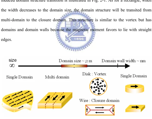
diameter. Because of the existence of ferromagnetic exchange coupling between spins, the spins naturally arrange themselves in the same direction, forming a single domain. However, as the diameter decreases, an increase in the magnetic free poles at the disk boundary causes the system energy to increase. In order to effectively lessen the density of the free poles, the formation of the multi-domain is necessary thereby reducing the system energy. When the disk size decreases to the domain size (~mm), but is still larger than the domain wall width (~nm), the closure configuration will be in the most stable state which is called the vortex state. As the disk size is reduced to below the domain wall width, the single domain state will reoccur. This sample size induced domain structure transition is illustrated in Fig. 2-1. As for a rectangle, when the width decreases to the domain size, the domain structure will be transited from multi-domain to the closure domain. This structure is similar to the vortex but has domains and domain walls because the magnetic moment favors to lie with straight edges.
Fig 2-1: Schema of domain structure related to the dimensions of a disk and a wire.
2-1-1 Fundamental magnetic energies
In this section, several magnetic energies are introduced [1], including exchange (Eex), magnetostatic (Emag), anisotropy (Eani), and Zeeman (EZ). In principle, domain formation results from the competition between these energy terms and magnetization hysteresis loop can be calculated by minimizing the sum of these energies.
Exchange energy
The origin of Eex is the spin-spin and spin-orbital interactions. The sum of all interactions is reduced using symmetry rules and orbital overlap to generate an effective spin-spin interaction. The exchange interaction is in short range and assumes that only interactions with the nearest neighbors are important. Eex can be described in terms of the exchange constant C. The energy per unit volume can be determined for a specific crystal lattice using:
∫
∞ ∞ − ∇ + ∇ + ∇ =C m m m dv Eex [( x) ( y) ( z) ] 2 1 r 2 r 2 r 2 (2-1)where C =2JS2c a, J is the exchange integral linking the atomic spins S and a is
lattice constant. Mr =mxiˆ+myˆj+mzkˆ is the magnetization vector. For
ferromagnetic materials, J is positive and the lowest energy state occurs when the spins are parallel to each other. c is a geometric factor associated with the crystal structure of the material (c = 1 for S.C., c = 2 for B.C.C., c = 4 for F.C.C., c = 2 2
for H.C.P.).
If one ferromagnet is in contact with another, an exchange interaction may couple these two media. The coupling strength can not be derived from the bulk properties, but depending on the interface. This interfacial exchange energy can be in
comparison with the bulk exchange and can be described by the following expression: ] ) ( 1 [ ) 1 ( 2 2 1 2 2 1 1 m m sC m m C s Eex= − r ⋅ r + − r ⋅ r (2-2)
Here mr1 and mr2 are the unit magnetization vectors of two materials at the surface,
C1 and C2 are the coupling constant [3]. s is the area of the interface. This energy
plays an important role only in the multilayer and trilayer systems [4].
Anisotropic energy
From classical point of view, the spin of each atom is isotropic and hence, its energy does not depend on the direction in space. In reality, most spins may lie along a preferable direction, especially for some magnetic materials. The energy of a ferromagnet may depend on the direction of the magnetization relative to the structural axes of the material and is called as the anisotropic energy. This energy could be classified to crystalline anisotropy and induced anisotropy. The latter describes the effects of deviations from ideal symmetry as for example because of lattice defects or partial atomic ordering. The former results from spin-orbital interaction which depends on the crystal structure. Because of the arrangement of atoms in crystalline materials, on certain axes, overlapping by the electron clouds is more serious. On these axes, the stronger spin-orbital interaction causes the crystalline fields to be created and the magnetization along certain orientations is energetically preferred. In the case of a simple cubic crystal, the crystal anisotropic energy (Ecry) can be written as:
2 2 2 2 2 2 2 2 2 2 1[ x y y z x z] x y z cry vK m m m m m m vK m m m E ≈ + + + (2-3)
where Ki is the crystalline anisotropy constant for the ith term, v is the volume of the body. The value of constant K1 is almost in the range of 105erg/cm3 for different
materials. K1>0 for Fe, the easy axes along (100), while K1<0 for Ni and the easy axes are along the body diagonals (111).
Another anisotropic energy term applies only to the surface magnetization was first introduced by Néel [5]. In a structurally isotropic medium, the surface anisotropy energy (Es) can be expressed to first order as:
] ) ˆ ( 1 [ 2 n m K v Es = s − r⋅
(2-4)
where nˆ is the surface normal and mr is the unit magnetization vector at the surface.
The order of magnitude of coefficient Ks is between 1 and 0.1 erg/cm2 [6]. For bulk samples, the effect of surface anisotropy is negligible because the surface magnetization is coupled by exchange forces to the bulk magnetization. It becomes important for thin film and nanoparticle systems.
External field (Zeeman) energy
EZ is simply the energy of the magnetization in an externally applied magnetic field. This energy has its minimum when the magnetization is along the external field and can be expressed as:
∫
⋅−
= M H dv
EZ r rexternal
(2-5)
Stray field (demagnetizing) energy
The origin of the Emag is the dipole-dipole interaction. For certain uniform magnetic bodies, they must have magnetic fluxes of M that terminate on their surfaces. From the Maxwell’s equations, the stray field (or the demagnetizing field Hd ) will be generated by the non-zero divergence of the magnetization M. This energy can be given by:
∫
⋅ − = sample d mag M H dv E r r 2 1(2-6) This energy is positive and the integral expresses the energy of a dipole Mdv in the field Hd created by the other dipole. The factor of 1/2 is there to keep off double counting over the dipoles.
In a uniformly magnetized ellipsoid, the demagnetizing field Hd is uniform and linearly related to the magnetization by the symmetrical demagnetizing tensor Nd, namely, Hd = -NdMs. Nd can be diagonalized if the magnetization points to a principle axis. For a general ellipsoid with a > b > c, where a, b, and c are the ellipsoid semi-axes, the demagnetizing factors along the semi-axes are Na, Nb, and Nc, respectively. The demagnetizing factor Na is given by the integral [7]:
η η η η η πabc a a b c d Na 1 0 2 2 2 2 ) ( )( )( )] [( 2
∫
∞ + + + + − =(2-7)
η is an arbitrary variable. Analogous expressions apply to Nb and Nc. The sum of all three factors is always equal to 4p.
♦ Sphere (a = b = c).Na =Nb = Nc =4π3 (2-8) ♦ Prolate ellipsoid (a >> b = c). This ellipsoid is often seen as an approximation for a nanowire with circular cross section. When the aspect ratio is defined as m = a / c, its demagnetizing factors are given by
⎥ ⎥ ⎦ ⎤ ⎢ ⎢ ⎣ ⎡ − − − + − − − = = ⎥ ⎥ ⎦ ⎤ ⎢ ⎢ ⎣ ⎡ − − − − + − − = ) ) 1 ( ) 1 ( ln( ) 1 ( 2 1 ) 1 ( 2 4 1 ) ) 1 ( ) 1 ( ln( ) 1 ( 2 1 1 4 2 1 2 2 1 2 2 1 2 2 2 1 2 2 1 2 2 1 2 2 m m m m m m m m N N m m m m m m m N c b a π π (2-9)
♦ Slender ellipsoid (a >> b > c). This ellipsoid is often seen as an approximation for nanowires deposited into templates with noncircular cross sections. Its demagnetizing factors are given by
) ( 4 ) 3 ( ) 4 ln( ) ( 2 1 ) ( 4 ) ( 4 ) 3 ( ) 4 ln( ) ( 2 1 ) ( 4 ] 1 ) 4 )[ln( ( 4 2 2 2 2 2 c b a c b bc c b a a bc c b b N c b a c b bc c b a a bc c b c N c b a a bc N c b a + + + + − + = + + + + − + = − + = π π π (2-10)
Because the demagnetizing energy is strongly influenced by the shape and has a uniaxially anisotropic character, it is often called shape anisotropy. Fig. 2-2 shows the calculation of the demagnetizing factors of the prolate ellipsoid which is dependent on the aspect ratio. When the nanowire has the high ratio of wire length to radius, it can be approximately regarded as the prolate ellipsoid with the high aspect ratio. In this case, the demagnetizing factor along the hard axis, perpendicular to the wire axis, equals 2p, and the demagnetization factor along the easy axis, parallel to the wire axis, is 0. Thus, the difference of the shape anisotropic energy between the two axes is pMs2.
Fig 2-2: The demagnetizing factor Nd of a prolate ellipsoid as a function of its
2-1-2 Domain structure in wires
In this section, we discuss remanent domain structure of a wire under the consideration of minimizing the total energy. If the entire magnetization of a wire is uniformly aligned with the long axis, which is also the easy axis of the crystalline anisotropy, the exchange and the crystalline anisotropy energy are both zero. The magnetostatic energy is maximized since the magnet acts like a single giant dipole. In order to minimize the total energy, a reduction of the magnetostatic energy is necessary and hence, the closure domain forms naturally. Both anisotropy and exchange energies increase due to the domain wall regions but the magnetostatic energy decreases significantly. It seems that the total energy can be further reduced by the formation of an additional domain, but at cost of an increase in the other energy. The formation of domain structure is strongly influenced by the dimensions and the shape of a wire. Later, we discuss theoretically domain structure of a wire by an approximation of a prolate ellipsoid with geometrical factors of a wire. For a prolate ellipsoid, the boundary between single domain and non-uniform states can be analytically determined. As for the case of a thin film element with sharp corners, we discuss domain structure based on the two dimensional approximation in theoretical aspect.
Prolate ellipsoidal approximation
We regard a wire as a prolate ellipsoid and initially assume that the entire magnetization is aligned uniformly with the long axis, which is also the easy axis of the crystalline anisotropy. The magnetostatic energy calculated by Eqs. (2-6) and (2-9) can be written as:
v M N E Euniform mag a s 2 2 1 = = (2-11) where v is the volume. When the magnetization is non-uniform, it is difficult to evaluate the magnetostatic energy exactly, but it may often be sufficient to have a reliable estimate for its value between two bounds. Brown has devised a rather general method for finding both upper and lower bounds [1,8]. To obtain such a lower bound, the magnetostatic energy is replaced by
∫
∫
⋅∇Φ − ∇Φ = ≥ space sample LB mag E M dv dv E ( )2 ' 8 1 π r(2-12)
M is the actual distribution for which the magnetostatic energy is to be calculated and
the " =−∇Φ
H is the true field due to some other distributions. Φ is the scalar
potential. The first integral is over the ferromagnetic body and the second integral is over the whole space. This expression was proven to be smaller than the actual magnetostatic energy of any distribution. It provides a lower bound to the magnetostatic energy of a given magnetization distribution M, in terms of an arbitrary field "
H . Here we choose H as the field of a uniformly magnetized ellipsoid and "
lead to ] [ 2 1 2 2 2 2 c c b b a a s LB vM N m N m N m E = + + (2-13)
where ma,b,c is the component of a unit vector in the prime axis and
∫
= v m dv
ma,b,c (1 ) a,b,c . Now considering the constraint 1
2 2 2 + + = c b a m m m and
using the Lagrangian multiplier method to find the minimum of ELB. Moreover, Brown claimed that the state of lowest energy of a ferromagnetic body, whose size is less than a certain critical size, is one of uniform magnetization. Therefore, for any distribution of M whose magnetostatic energy is always larger than Euniform, as well as
ELB ≧ Euniform. From this inequality we can obtain the critical size which marks the boundary between uniform and non-uniform states.
a s critical N C M q L = (2-14)
where q is the smallest solution of the Bessel functions and is related to the aspect ratio m of the prolate ellipsoid. q = 1.8412 + 0.48694/m – 0.11381/m2. The red dashed line in Fig 2-3 is the critical length versus the aspect ratio for a permalloy ellipsoid by Eq. (2-14). The saturated magnetization Ms =830emu/cm3 and the exchange constant
C = 2.1x10⁻⁶erg/cm were used. These two parameters are suitable for a confined structure and will be discussed in the section 3-3. The magnetization prefers to align uniformly for a wire with a high aspect ratio. While at a fixed aspect ratio, the uniform state would be observed in a shorter wire.
0 20 40 60 80 0 10 20 30
Cri
tica
l Leng
th
(
μ
m
)
Aspect ratio m
Single domain Non-uniformly magnetized state 0 20 40 60 80 0 10 20 30Cri
tica
l Leng
th
(
μ
m
)
Aspect ratio m
Single domain Non-uniformly magnetized stateFig 2-3: The theoretically domain diagram of a prolate ellipsoid as a function of the aspect ratio and the critical length.
Edge induced domain
For a rectangular thin film element, there are straight edges and sharp corners resulting in different domain configuration from an ellipsoid. The calculation of magnetostatic energy is complex and the numerical evaluation is usually used. The induced domain appears at the corner, due to the magnetic pole avoidance. Here, the edge induced domain in a wire is discussed based on a two-dimensional approximation which is suitable for a thin film of a soft magnetic material.
If the dimension of a rectangular thin film element with zero crystalline and induced anisotropy is much larger than the single domain limit, a flux closure magnetization configuration with vanishing magnetostatic energy may be favored. In such a pattern, the magnetization lies parallel to the film surface and is diverging free in the interior and at the edges. Therefore, domains and domain walls can be obtained under the consideration of the boundary conditions and the principle of pole avoidance. Van den Berg developed a comprehensive analysis on the prediction of the possible range of these domains and the position of domain walls for such thin film elements with arbitrary shape [9]. He proved that a stray field free magnetization pattern can be constructed when following the below conditions.
z Take circles that touch the edges at two (or more) points and lie otherwise
completely within the figure. The centers of all such circles form the domain walls.
z If a circle touches the edges in more than two points, its centre forms a domain
wall junction.
z In every circle the magnetization direction must be perpendicular to each
touching radius.
For a rectangle, the domain pattern can be illustrated as a flux closure structure which is the well known Laudau-Lifshitz pattern. In Fig. 2-4, the circles marked 1, 2, and 3 touch at least two points at the edge and lie completely within the rectangle.
Their centers 1’, 2’, and 3’, respectively, are located at the domain walls. Moreover, circle 2 is touching the edge at three points implying that its center 2’ coincides with a domain-wall junction. As for the circles 4 and 5, they are touching two edge points; however, they are lying only partly within the object, so that centers 4’ and 5’ are not at domain walls. Following the third condition, the magnetization direction must to be perpendicular to each touching radius resulting in the closure pattern.
Fig 2-4: A formation of a flux closure pattern in a rectangle.
Subsequently, we try to find the energy gain by the flux closure domain relative to the single domain state, and below which sample size the flux closure domain become unstable, taking into account the domain wall energy. For a uniformly magnetized rectangular thin film element, the total energy is simply the Emag. Although a thorough calculation of Emag is necessary to be approached by the finite element calculation [10], we regard the rectangle as a prolate ellipsoid and use Eq. (2-11) to make calculations much easier. A flux closure domain may carry a zero net magnetization and hence, the total energy is the only domain wall energy and can be written as:EFC =[(2 2−1)w+l]⋅t⋅γ where w, l, and t are the width, length, and
thickness of a rectangle, respectively. γis the domain wall energy per unit area. The single domain limit Lcritical is obtained by equating the domain wall energy with Eq.
(2-11), as following: ) 1 2 2 ( ) 2 1 ( 2 − − = γ l M N l L s a critical (2-15)
The single domain limit is thus determined by the interplay between the domain wall energy and the magnetostatic energy.
2-2
Magnetization reversal in wires
Magnetization reversal is a process which refers to the variation of magnetic configuration under magnetic fields, pulse currents, and pulse fields, etc. The process in thin films and bulks has been widely investigated. Recent advantages in the nanofabrication methods have made the possibility of studying the magnetism at small length scale.
In our study, we focus on the reversal process of a wire. For a wide wire, these typical reversal mechanisms of a thin film, such as the nucleation and annihilation of domains and propagation of domain walls still play an important role in the reversal process. When a wire width is less than the critical length, the single domain is an energetically favorable state. The question of magnetization reversal mechanisms for such wire is whether the magnetic moment rotation is always in unison. Brown provided a set of differential equations from minimizing the additional energy contributed from the magnetization perturbation and claimed that the eigenfunctions of these equations are the state of system during reversal and the eigenvalues are the
switching fields (Hsw) at which field the magnetization has a significant change[11]. The physical system will choose the one yielding the least Hsw since the mode is more achievable. For a prolate ellipsoid, three eigenmodes are proposed such as the following: coherent rotation, magnetization curling, and magnetization buckling.
Their magnetization arrangements and the theoretical anticipation of the relationship between the Hsw and the wire width are presented in Fig. 2-5. In the coherent rotation mode, all magnetic moments remain parallel to each other during the reversal process. By contrast, the buckling mode and the curling mode have a zigzag configuration in the plane and a vortex structure in the cross-section, respectively. The switching field appears to be uncorrelated with dimensions for coherent rotation. The switching field decreases with increasing wire width as a reciprocal relation when the reversal is completed via the magnetization curling. A threshold between both is the exchange length lex,2 C /Ms. For a semi-wire width larger than lex, the reversal
occurs through curling. While a semi-wire width is smaller than lex, the coherent
rotation is expected by the Stoner–Wohlfarth model [12]. Because the buckling mode occurs only in a narrow-sized interval, these two modes are usually seen as the only switching modes that can occur.
Later, several reports using the micro-magnetic simulation method show that the complete magnetization moment rotation during the reversal is not always uniform. The magnetization reversal can occur through a creation of domain wall pairs and then sweep across a wire [13-15]. Furthermore, a number of studies show that thermal fluctuation can activate magnetization reversal resulting in a non-uniformly spatial magnetization distribution [16,17].
Fig 2-5: (Left) Theoretical plot of the reduced switching field as a function of the reduced semi-wire width for the coherent rotation, the magnetization curling, and the magnetization buckling. (Right) Illustration of magnetization reversal for the corresponding mechanism [18].
2-2-1 Magnetization reversal by Uniform rotation
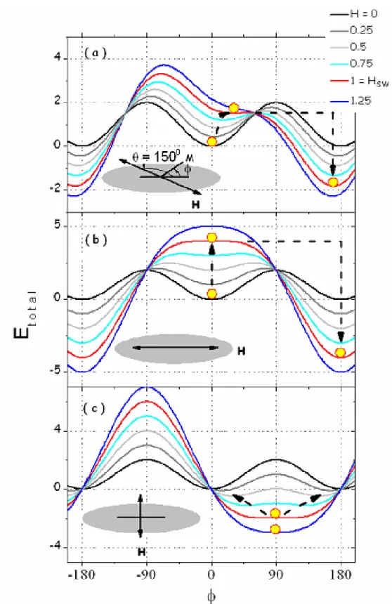
Coherent rotation – Stoner Wohlfarth model
The magnetic moment rotates in the same angle everywhere and it is therefore known as the coherent rotation mode. It can be expressed in terms of the classic Stoner-Wohlfarth model [12]. In this model, a particle is assumed that exchange energy holds all spins tightly parallel to each other and there is a uniaxial anisotropy. Then, during the magnetization reversal the total energy consists of only Eani and EZ.
For a simply second-order uniaxial anisotropy, the total energy can be written as: ) cos( sin2φ − θ −φ =vK vM H Etotal u s (2-16)
where φ and q are the angles of magnetization and applied field with respect to the easy axis of magnetization, respectively. Ku is the uniaxial anisotropic constant. When the applied field is zero, the Etotal exhibits a periodicity of π . There are minima and maxima at φ =nπ with n=0,1,2… and 0.5,1.5,2.5…., respectively. The
magnetization always lies along the easy axis at remanence. As illustrated in Fig. 2-6, the Etotal is plotted as a function of q, H, and φ according to Eq. (2-16). The magnetization reversal is determined by the local minimum and derivative of Etotal. Here, we consider three different orientations of magnetic field relative to the easy axis. Let us start with the simple case that magnetic field is along the easy axis (q=0o),
as shown in Fig. 2-6(b). At remanence, magnetic moment is along the easy axis and E is a local minimum at φ =0o. As the magnetic field is reversed, although E
total increases, the local minimum of Etotal remains at
o
0 =
φ before reaching the Hsw. Until the magnetic field is equal to Hsw, φ =0o becomes a local maximum and magnetic moment rotate suddenly by 180o. For a new local minimum of E
total at
o
180 =
φ with further increasing magnetic field, the moment stays at φ =180o. In
another extreme case that magnetic field is perpendicular to the easy axis (q=90o) as
shown in Fig. 2-6(c). The magnetization is along the direction of the applied field when the applied field is large enough to saturate the magnetization, implying that
o
90 =
φ is the local minimum of the Etotal. With reducing the applied field, φ =90o is no longer the local minimum, resulting in smooth rotation of magnetization until along the easy axis (φ =0o or 180 ). There are two possible paths toward o φ =0o
neither along nor perpendicular to the easy axis. As shown in Fig. 2-6(a), the magnetic field makes an angle of 30o with respect to the easy axis. At remanence, magnetic
moment is along the easy axis and E is a local minimum at φ =0o. As the magnetic
field is reversed, the local minimum of E moves slightly from φ =0o to φ =30o
with increasing magnetic field resulting from the competition of the shape anisotropy and magnetic field. When the magnetic field is equal to Hsw, the magnetic moment switches to an angle φ =150o, where has the lowest energy. Fig. 2-6(a) shows this
switching behaviors indicated by the dashed line.
The switching field can be calculated by the analysis of the stability of the total energy. For given values of q and H, the magnetization lies at an angle φ where the energy is a minimum locally. The magnetization direction must fulfill that the first derivative of Etotal with respect to φ is zero. Using the reduced
fieldh=H (2Ku /Ms)and the reduced magnetizationm=M Ms =cos(θ −ϕ), this
equation can be written as:
5 . 0 2 2 5 . 0 2) cos2 (1 2 )sin2 2 (1 ) 1 ( 2m −m θ + − m θ =± h −m (2-17)
The magnetization hysteresis loop can be calculated from this equation by solving for
m as a function of h. Then, Hsw as a function of q can be obtained
when∂h ∂m=0and∂2Etotal ∂φ2 >0, and can be written as:
2 3 3 2 3 2 ) sin (cos 2 − + = θ θ s u sw M K H (2-18)
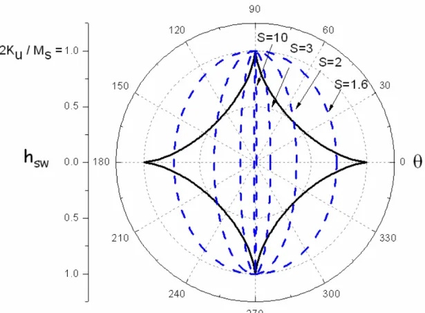
A polar plot of reduced Hsw(q) shown in Fig. 2-7 by the solid line is the famous Stoner-Wohlfarth astroid. There is four-fold symmetry of Hsw(q). Hsw is a maximum when the applied field is parallel and perpendicular to the easy axis and is a minimum at q=45o±90o, implying the magnitude of H
operating at this point. This concept has been used in the writing process of MRAM.
Fig 2-6: The total energy as a function of the magnetization angle for several magnetic field values based on Stoner-Wohlfarth model. (a) q = 150o (b) q = 0o (c) q = 90o.
2-2-2 Nonuniform magnetization reversal
As seen in Fig. 2-5, magnetization should reverse by coherent rotation for small samples. For larger samples, nonuniform reversal modes are more likely. Two principal nonuniform reversal modes of an ellipsoid are curling mode and buckling mode. The latter was identified only in a narrow-sized interval. We ignore it here because of its minor importance. The former is discussed in the following.
Magnetization Curling
Curling mode assumes that the magnetization direction rotates in a plane perpendicular to the anisotropy axis of the wire, effectively reducing the stray field. The feature of this mode has been presented in Fig. 2-5. Although analytical solutions of the magnetization hysteresis loop by curling mode are not available. Aharoni assumed that magnetic moments rotate uniformly before switching and solved the Brown’s differential equations based on the curling mode to obtain the angular dependence of the switching field for a prolate ellipsoid [19]. The relation is given by
θ θ π 2 2 2 2 2 2 2 2 cos ) 2 ( sin ) 2 ( ) 2 )( 2 ( 2 S k D S k D S k D S k D M H c a c a s sw − + − − − = (2-19)
where Da = Na 4π and Dc =Nc 4π are the demagnetizing factors of a prolate
ellipsoid along the major and minor axes, respectively, which are presented in section 2-1-1.The parameter S is the reduced radius: S = 2r/lex, r is the minor semi-width. k =
q2/p where q is the same geometrical factor used in Eq. (2-14). The switching field
for several values of S as a function of q is plotted as dashed lines in Fig 2-7. In the case of S=2, switching field of magnetization curling is a minimum when the applied
field is parallel to the easy axis and has an increasing trend when the magnetic field is applied approaching the hard axis. As we can see, the switching field of magnetization curling is less than coherent rotation when q<45o±90o, implying the reversal occurs
via magnetization curling at small angle but via coherent rotation at large angle. The amount of the angle with the reversal completed via coherent rotation increases with decreasing S. For S<1, the reversal is completely through the coherent rotation and the switching field is given by the Stoner-Wohlfarth model.
Fig 2-7: Angular dependence of the switching field of a prolate ellipsoid for several reduced radii S. For S<1, the switching field is given by the Stoner-Wohlfarth model and is presented by the solid line.
Propagation of domain walls
In section 2-1-2, we mentioned that the edge domain of a thin film element exists based on the principle of pole avoidance. Even for a rectangle with a high aspect ratio of a near single domain state, the edge domain is still observed. The behavior of these domain structures in applied fields have been theoretically investigated by Bryant and Suhl [20]. Their initial ideal was that the magnetic charges induced in an applied field should be distributed as in the analogous electrostatic problem. The magnetic charges are expected at the edges of the element like the electric charges reside on the surfaces of a conductor. Once the distribution of these magnetic charges is known, the domain pattern can be calculated numerically for any field. As for a rectangle with a uniform magnetization for almost all volume except both ends, the propagation and the annihilation of domain walls play a major role during the magnetization reversal. The angular dependence of the switching field may be appropriately expected by 1/cosq, according to the projection of the magnetic field on the wire axis [21].
2-3 Magnetoresistance of ferromagnetic wires
The definition of magnetoresistance (MR) is the change in the resistance induced by an applied magnetic field. There are a number of different kinds of MR, such as Lorentz magnetoresistance (LMR), anisotropic magnetoresistance (AMR), giant magnetoresistance (GMR), colossal magnetoresistance (CMR), and domain wall magnetoresistance (DWMR), each with a different origin. Among them, AMR and DWMR have a major contribution for a single layer ferromagnetic specimen. Focusing on these two kinds of MR, their origin and behavior are discussed as follows.
2-3-1 Anisotropic magnetoresistance
The resistance of a material depends on its state of magnetization. This phenomenon is called magnetoresistive effect. The origin of the magnetoresistive effect in semiconductors and normal metals is the influence of the Lorentz force on the current path, with a result that the resistance is proportional to the square of the magnetic field. Apart from the ordinary magnetoresistive effect in semiconductors and normal metals, there is another effect in transition metals due to the spin-orbital interaction. In this effect the resistance depends on the orientation of the magnetization with respect to the direction of the electric current. The effect is often called the anisotropic magnetoresistance (AMR), which was first discovered by Kelvin [22].
It is convenient to explain AMR effect by taking into account the existence of the spin-orbital coupling and the anisotropic scattering mechanism of s and d electrons. In the case of the magnetic field direction with an angle relative to the current direction, the spin orbital interaction causes the resultant perturbed d-electron wave function to have a complex dependence on the angle. The transition probability of s electron to d orbital is large for electrons traveling parallel to the magnetic field. In the transition metal, the band structure is split into two different sub-bands of different orientations of the electron spins. When the 3d band is not fully filled, the transition of 4s electrons to 3d band is probable. The current of 4s electrons with smaller effective mass predominates the transport. The 3d electrons with large effective mass have low mobility. If there is a large transition probability of 4s electrons to 3d band, the increase of 3d electrons in the conduction current results in the decrease of conductance. Thus, when the current is parallel to the magnetic field direction, the
large transition probability leads to large resistance.
For a single crystalline metal with saturated magnetization, the Ohm’s law is described by the following expressionEi ij M Jj
r r r ) ( ρ
= , where Eris the electric field,
Jris the current density, and ρis the tensor of the resistivity. Taking into account the
crystal symmetry, Thomas obtained the resistivity tensor for a simple case that the magnetic field is in the film plane (x-y plane) [23]:
⎥ ⎥ ⎥ ⎦ ⎤ ⎢ ⎢ ⎢ ⎣ ⎡ − − + Δ Δ + t H H H l t H l t ρ φ ρ φ ρ φ ρ φ ρ φ ρ φ ρ φ ρ φ ρ φ ρ φ ρ cos sin cos sin cos 2 sin sin 2 sin cos sin 2 2 2 1 2 1 2 2 (2-20)
whereρtandρlare the resistivity at the current direction perpendicular and parallel to the magnetization direction, respectively.Δρ =ρl −ρt. ρ is the Hall coefficient. H
φis an angle between the orientation of the magnetization and the current direction. When the current is in the x-axis, the resistivity in the x-axis is described by the expression. φ ρ ρ φ ρ ( )= +Δ cos2 t xx (2-21)
It is the general formula of AMR effect. The resistivity in the y-axis is written as
φ ρ θ
ρ ( )= 21Δ sin2
xy (2-22)
It is the so-called Planar Hall effect. The angular dependences of resistivity for both effects are presented in Fig.2-8. Both cases show an periodicity of π . AMR and PHE have maxima at φ =nπ with n=0,1,2… and 0.25,1.25,2.25…, respectively, and
Fig 2-8: Schematic plot of the angular dependences of the resistivities, AMR (red) and PHE (blue), respectively.
2-3-2 Domain wall resistance
Domain wall resistance arises from the scattering when electric current passes through a domain wall. In general cases, the contribution of DW scattering to the MR is concealed by conventional sources of low temperature MR such as AMR and LMR in a ferromagnetic system. In order to isolate DWR, it is necessary to create artificial domain walls using a unique pattern such as adding a neck to the wires [24], designing zigzag structures [25], forming a striped domain by thickness modulation [26] or exchange biases [27], and implementing an elaborate magnetic field history process [28]. Although DWR was observed in various systems, both positive[24-28] and negative[29] values were reported with their theoretical justifications [30-32]. Up to now, the sign and the magnitude of the DWR and the fundamental mechanisms of DW scattering are still controversial. In this section, we introduce the historical
theories about the positive DWR.
Spin mistracking effect
The intrinsic DWR arising from the spin polarized current passing through a domain wall has been developed by two methods, semi-classical and fully quantum mechanical, to predict the magnitude of this effect. When electrons pass through a domain wall, the electron spin will precess around the rotating exchange field and lags behind in orientation with respect to the local magnetization, as seen in Fig. 2-9. Viret estimated the average of this angle via the exchange field rotating through in half of a Larmor precession. He treated the spin vector classically and found that the mean free path depends on the spin-dependent scattering rate and the cosine of the behind angle [33]. Then, DWMR can be written as:
2 2 ( ) ) 1 ( 2 ex f DW DE hv P P R R − = Δ (2-23)
P is the spin-dependent scattering ratio, v is the Fermi velocity, D is the domain wall f
width, and h is Planck constant. For the example of Ni, the value of DWMR predicted by this semi-classical model is about 4×10⁻⁵ and follows the ~1/D2 relation.
Fig 2-9: Numerical simulation of the spin trajectory for the electron spin transiting through domain walls in Ni. The electron spin orientation is showed in red and the local exchange field variation in blue [31].
Levy and Zhang rebuilt this model by replacing the simple rotating frame with a fully quantum mechanical analysis [30]. In their analysis, they used the same Hamiltonian that is used to describe the GMR in a magnetic multilayer. In addition to the potential and the kinetic energy terms, there is a spin dependent term involving the spin operator and the local magnetization distribution. When the magnetization is uniform, the Hamiltonian can be diagonalized along any chosen axis by making a rotation of the spin operator using the rotation operator. The resulted Hamiltonian can be recovered to the same form. However, when the magnetization is not uniform, like in the domain wall region, there is an extra term in the Hamiltonian as carrying on the diagonalisation. This extra term arises from a perturbation of the wavefunctions and becomes the source of an extra resistance. In a one-dimensional Bloch or Néel domain wall where the angle change of unit length θ(x)=xπ D, implying that magnetic
moment rotate linearly from one direction to the opposite direction through the wall width D, two useful formulas were found, corresponding to two basic measurement geometries, CIW and CPW where the current flow parallel and perpendicular to the wall, respectively. Eqs. (2-24) and (2-25) describe the DWMR in the conditions.
↓ ↑ ↓ ↑ − = Δ ρ ρ ρ ρ ξ2 ( )2 5 ) ( CIW DW R R (2-24) ] 10 3 [ ) ( 5 ) ( 2 2 ↓ ↑ ↓ ↑ ↓ ↑ ↓ ↑ + + − = Δ ρ ρ ρ ρ ρ ρ ρ ρ ξ CPW DW R R (2-25) ↑↓
ρ is the resistivity for spin ↑ and ↓ of the ferromagnet. 1 ρ =1 ρ↑ +1 ρ↓ is the conductivity of the ferromagnet without domain walls. The mistracking parameter
mDJ kF 4
2
h
π
ξ = , J is the exchange splitting energy. If one wants to obtain a large DWR, it is necessary to make ξ as large as possible, one way that this can be achieved is to have a narrow wall. For the example of Co, the value of DWMR
predicted by this model is 0.3-1.8% for a CIW case and 2-11% for a CPW case, and DWR also follows the ~1/D2 relation.
References:
1. A. Aharoni, Introduction to the Theory of Ferromagnetism, Oxford University Press, Oxford, 2000.
2. B. D. Cullity, Introduction to magnetic materials, Addison-Wesley publishing company, 1972.
3. P. Bruno, Phys. Rev. B 52, 411 (1995).
4. J. Slonczewski, J. Magn. Magn. Mat. 150, 13 (1995). 5. L. Néel, C. R. Acad. Sci. Paris 237, 1468 (1953).
6. D. S. Chuang, C. A. Ballantine, and R. C. O’Handley, Phys. Rev. B 49, 15084 (1994).
7. J. A. Osborn, Phys. Rev. 67, 351 (1945). 8. A. Aharoni, J. Appl. Phys. 63, 5879 (1988).
9. H. A. M. van den Berg, IBM J. Res. Dev. 33, 540 (1989).
10. P. Rhodes and G. Rowlands, Proc. Leeds Phil. Soc. 6, 191 (1954). 11. W. F. Brown, Phys. Rev. 105, 1479 (1957).
12. E. C. Stoner and E. P. Wohlfarth, Philos. Trans. R. Soc. London, Ser. A 240, 599 (1948) [reprinted in IEEE Trans. Magn. 27, 3475 (1991)].
13. R. Ferre´, K. Ounadjela, J. M.George, L. Piraux, and S. Dubois, Phys. Rev. B 56, 14066 (1997).
14. J.McCord, A. Hubert, G. Schröpfer, and U. Loreit, IEEE Trans. Magn. 32, 4806 (1996).
15. M. Brands, R. Wieser, C. Hassel, D. Hinzke, and G. Dumpich, Phys. Rev. B 74, 174411 (2006).
16. J. S. Broz, H. B. Braun, O. BrodBeck, and W. Baltensperger, Phys. Rev. Lett. 65, 787 (1990
).
17. H. B. Braun, Phys. Rev. B 50, 16501 (1994).
18. E. H. Frei, S. Shtrikman, and D. Treves, Phys. Rev. 106, 446 (1957). 19. A. Aharoni, J. Appl. Phys. 82, 1281 (1997).
20. P. Bryant and H. Suhl, Appl. Phys. Lett. 54, 2224 (1989).
21. F. Cebollada, M. F. Rossignol, D. Givord, V. V. Boas, and J. M. González, Phys. Rev. B 52, 13511 (1995).
22. W. Thomson, Proc. R. Soc. 8, 546 (1857). 23. G. Thomas, Physica 45, 407 (1969).
24. S. Lepadatu and Y. B. Xu, Phys. Rev. Lett. 92, 127201 (2004).
25. T. Taniyama, I. Nalatani, T. Namikawa, and Y. Yamazaki, Phys. Rev. Lett. 82, 2780 (1999).
26. W. L. Lee, F. Q. Zhu, and C. L. Chien, Appl. Phys. Lett. 88, 122503 (2006). 27. D. Buntinx, S. Brems, A. Volodin, K. Temst, and C. V. Haesendonck, Phys. Rev.
Lett. 94, 017204 (2005).
28. U. Ebels, A. Radulescu, Y. Henry, L. Piraux, and K. Ounadjela1, Phys. Rev. Lett.
84, 983 (2000).
29. U. Rüdiger, J. Yu, S. Zhang, A. D. Kent, and S. S. P. Parkin, Phys. Rev. Lett. 80, 5639 (1998).
30. P. M. Levy and S. Zhang, Phys. Rev. Lett. 79, 5110 (1997).
31. J. F. Gregg, W. Allen, K. Ounadjela, M. Viret, M. Hehn, S. M. Thompson, and J. M. D. Coey, Phys. Rev. Lett. 77, 1580 (1996).
32. G. Tatara and H. Fukuyama, Phys. Rev. Lett. 78, 3773 (1997).
33. M. Viret, D. Vignoles, D. Cole, J. M. D. Coey, W. Allen, D. S. Daniel, and J.F.Gregg, Phys. Rev. B 53, 8464 (1996).
3 Experimental Details
In the investigation of domain structure and magnetization reversal on micron and sub-micron magnetic structures, we take several experimental techniques. This chapter is divided into two parts. First part is techniques of device fabrication. Second part is the measurement techniques involving magnetoresistance measurement and magnetic domain observation.
3-1 Device fabrication
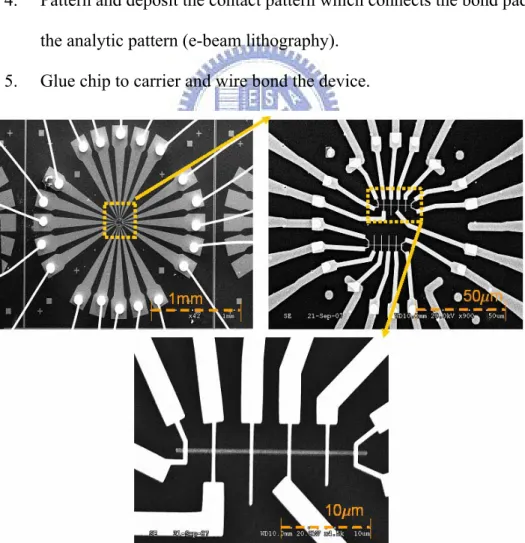
The micron and sub-micron magnetic samples in the experiment are fabricated using two kinds of lithography techniques. One is Photo-Lithography (PL) which is the standard method of producing devices in the semiconductor industry. The other is electron beam lithography (EBL) which is a flexible technique for creating extremely fine patterns and is used principally in the support of mask making in the integrated circuit industry. Both lithography methods have similar fabrication procedures apart from the exposure source. An electron beam is used in EBL to expose the resist, whereas, in contrast, ultraviolet (UV) light is used in PL. Deposition of materials into the groove of the resist constructed by either EBL or PL is then carried out. Figure 3-1 shows a nanowire device at several levels of magnification so that the photo and e-beam lithography steps are all visible. Au(70nm) and Ti(10nm), which has good adhesion with (100) Si substrates, are stacked sequentially to form the electrode pads as seen in the top left figure. The entire deposition process is employed using thermal evaporation at a base pressure of 2.3×10⁻⁶ Torr. The dimension of one end of the electrode is about 200mm for wire bonding. As extending the other end of the electrode to the center of the device, the dimension is decreased to 5mm. As for the
analytic pattern in the submicron scale, the EBL is appropriately chosen. The material used in this study is ferromagnetic Permalloy (Ni80Fe20). Later a brief introduction
will be given to the lithography techniques described above together with the recipe used and the results.
The outline of the fabrication process is as follows:
1. Cleave a small chip (~6mm×6mm) from the Si wafer.
2. Pattern, deposit, and anneal the bond pads (photolithography).
3. Pattern and deposit the analytic pattern on mm and sub-mm scales (e-beam lithography).
4. Pattern and deposit the contact pattern which connects the bond pads and the analytic pattern (e-beam lithography).
5. Glue chip to carrier and wire bond the device.
Fig 3-1: SEM images of a typical device at different magnifications. The upper left image shows the bond pad structure with wire bonds. The other two images show the contact and the analytic pattern.
3-1-1
Photolithography
Photolithography is the process of using UV light to transfer geometric shapes on a mask to a light-sensitive chemical on the surface of a substrate. The ideal resolution of this technique is limited by the wavelength of the light that is used. In our experiment, ABM Model 60 DUV/MUV/NearUV Mask Alignment and Exposure System is used. A 500W high pressure mercury arc lamp provides an intensity of around 60mW/cm2 for h-line (400nm) and around 35mW/cm2 for i-line (365nm). The
i-line is filtered from the spectrum of mercury with the intensity around 20~25mW/cm2 for our process in which the exposure time is ~ 10sec. Attachment
between the sample and mask is in contact mode. Using this mode, certain faults of generating patterns during the imprint process, such as the wavy edge and the reduction of the pattern dimension caused by the deficient light dose, can be corrected. The photo-resist AZ5214 is used here. The polarity of this kind of resist can be reversed by a sufficiently exposure energy resulting in the formation of good undercut profiles for the advantage of lift-off step. The extreme resolution of the i-line source limited by the interference is about ~50nm. However, the actual conditions, such as the numerical aperture, the sensitivity of the chemical resist, and the method of applying the lift-off technique, cause the best resolution in this procedure to be around 0.6mm. Fig. 3-2 presents the two SEM images of photo-lithography patterns. The dimension of the outer pads is about 200mm and the dimension of the inner leads is about 5mm. The basic photolithography process recipe I have used is showed in the following.
The photolithography recipe
♦ Clean in acetone, alcohol, D.I. water and dry using nitrogen gas. ♦ Spin AZ5214 photo-resist, first at 1000rpm for 10sec and then at
5000rpm for 40sec. (This gives a ~ 1mm thick layer.). ♦ Soft bake at 90oC for 90sec.
♦ Expose at an energy density of 28mW/cm2 for 1 sec (i-line). (The
time required depends on the energy density of the i-line and the thickness of the resist.).
♦ Reverse bake at 120oC for 90sec. (A special property of AZ5214
is that the polarity can be reversed from positive to negative.). ♦ Perform a flood exposure for 20sec.
♦ Develop in AZ400 for ~ 20sec. Rinse in D.I. water for ~ 5sec, and then blow dry.
♦ Clean any residual resist using O2 plasma at 800V for 2min.
♦ Evaporate the materials and remove the resist by soaking in acetone and agitating using a mild ultrasonic.
♦ Finish by rinsing in D.I. water for ~ 3sec and then blowing dry.
Figure 3-2: SEM images of the typical photolithography pattern at different magnifications, 40(left) and 1200(right).