國 立 交 通 大 學
電機學院通訊與網路科技產業專班
碩士論文
平衡式數位移相器
Balanced Digital Phase Shifter
研究生 : 劉耿宏
指導教授 : 張志揚 博士
中華民國 九十九 年 六 月
平衡式數位移相器
研 究 生 : 劉耿宏 Student : Keng-Hung Liu
指導教授 : 張志揚 博士 Advisor : Dr. Chi-Yang Chang
國立交通大學
電機學院通訊與網路科技產業專班
碩 士 論 文
A Thesis
Submitted to College of Electrical and Computer Engineering
National Chiao Tung University
in partial Fulfillment of the Requirements
for the Degree of
Master
in
Industrial Technology R & D Master Program on
Communication Engineering
June 2010
Hsinchu, Taiwan, Republic of China
中華民國九十九年六月
i
平衡式數位移相器
研究生 : 劉耿宏 指導教授 : 張志揚 博士
電機學院通訊與網路科技產業專班
摘要
本篇論文提出以變換輸入模態來改變相位之相位轉換器,此相位轉換器在奇模與 偶模訊號輸入時,相位不同,利用這種特性,我們可以設計出所需要轉換之相位角 度。論文中提出 90˚, 45˚, 22.5˚角度的相位轉換器,並且利用四分之波長組抗轉換器 來實現 22.5 度之相位轉換器。
ii
Balanced Digital Phase Shifter
Student : Keng-Hung Liu Advisor : Dr. Chi-Yang Chang
Industrial Technology R & D Master Program of
Electrical and Computer Engineering College
National Chiao Tung University
Abstract
In this thesis, phase shifters change phases by changing input signal mode are proposed. The insertion phase is different when the input signal is even and odd. Using this property, we can design the angle we want to change. In this thesis, three phase shifters, namely, 90˚, 45˚, 22.5˚ are proposed. Moreover, the high impedance of 22.5˚ phase shifter is realized by quarter wave transformer.
iii
Acknowledgement
誌 謝
本篇論文的完成,最感謝的是指導教授張志揚老師在我念研究所時候的指導, 老師不管在研究或生活方面,都給予我相當實際有效的建議與幫助。在課業之餘, 更常常帶著實驗室的大家一起去騎腳踏車,培養健康的體能,以及一起吃飯談天, 跟老師聊天也都常常有意外的收穫及啟發,也紓解了日常生活的壓力。讓我的碩班 生涯,除了專業以外,更多了很多人生樂觀進取的態度,以及對於各種生活上大小 事情的體悟。因此相當的感謝老師。同時,感謝口試委員鍾世忠教授、孟慶宗教授 所提供的寶貴建議與指教,使本篇論文更加完善。 感謝實驗室學弟妹同儕與學長姐們,金雄、鈞翔、建育、哲慶、正憲、如屏、 忠傑、佩潔、楊達、聖智、德育、宛蓉、懿萱、鵬達、維欣。因為你們,實驗室充 滿歡愉的氣氛,讓本來嚴肅的研究生活,心情上頓時輕鬆不少。 特別感謝益廷學長在我研究遇到瓶頸時,能夠很不厭其煩的教導我並且幫助我 解決問題,你耐心細心且謙卑的精神,讓我相當感動。感謝同為96 級的昀緯,日常 關心及幫忙,讓我疲累時,有堅持下去的力量。感謝士峰學弟,讓我生活上豐富了 很多,也多了更多的體驗與朋友,這些對我而言,都相當彌足珍貴。另外,感謝在 我碩班生涯裏面,所有陪伴我,鼓勵我的朋友們,有你們的支持,當我遇到挫折的 時候,才能夠繼續努力下去。 最後要感謝的是我親愛的家人,爸爸,媽媽,以及弟弟。你們是我背後莫大的 支柱,能夠全心的專注在課業上,沒有其他煩惱,都要歸功於你們,非常感謝你們。
iv
Table of Contents
摘要 ... i
Abstract ...ii
Acknowledgement...iii
Table of Contents ...iv
List of Figures ...v List of Tables ...vii Chapter 1 Introduction ... 1 Chapter 2 Basic Theory... 8 2.1 Analysis and Characteristics of Uniform Line Equivalent Circuit [1] ... 8 2.2 Three Element Loaded Line [1] ... 12 2.3 Richard’s Transformation [2] ... 15 2.4 The quarter‐wave transformer [2]... 17 Chapter3 The proposed phase shifter... 19
3.1 Design procedure and Realization for 90 degree phase shifter ... 19
3.2 Design procedure and Realization for 45 degree phase shifter ... 25
3.3 Design procedure and Realization for 22.5 degree phase shifter ... 29
Chapter 4 Conclusion ... 34
v
List of Figures
Figure 1.1 half duplex, frequency division duplexing... 1
Figure 1.2 The Antenna array. ... 1
Figure 1.3 Switched Line Phase Shifter topology. ... 3
Figure 1.4 Loaded-line phase shifter. ... 4
Figure 1.5 Reflection phase shifter... 4
Figure 1.6 The 4-bit phase shift set. ... 5
Figure 1.7 3bit balanced digital phase shifter... 6
Figure2.1 Uniform unloaded line equivalent circuit... 4
Figure 2.2 lumped element equivalent circuit. ... 4
Figure 2.3 Switched Transmission Phase Shifter Section. ... 5
Figure 2.4 Graphical Representation of Transmission Phase Shifter Phase Length Change ... 6
Figure 2.5 The Three Element Loaded Line Phase Shifter ... 9
Figure 2.6 Richard’s transformation. (a) For an inductor to a short-circuited stub. (b) For a capacitor to an open-circuited stub... 11
Figure 2.8 A transmission line terminated in load impedance RL. ... 16
Figure 2. 9 A transmission line terminated in load impedance RL ... 17
Figure 3.1 The overall circuit diagram. (a) In circuit simulation tool, ADS. (b,c) In EM simulation tool, Sonnet. . ... 19
Figure 3.2 Sonnet Simulation: S parameter for 90 degree phase shifter . ... 20
Figure 3.3 Sonnet Simulation: phase error for 90 degree phase shifter... 21
Figure 3.4 Photograph of 90 degree phase shifter. ... 21
vi
response for 90 degree phase shifter... 23
Figure 3.6 The overall circuit diagram. (a) In circuit simulation tool, ADS. (b) In EM simulation tool, Sonnet. ... 24
Figure 3.7 Sonnet Simulation: S parameter for 45 degree phase shifter 25
Figure 3.8 Sonnet Simulation: phase error for 45 degree phase shifter... 26
Figure 3.9 Photograph of 45 degree phase shifter ... 26
Figure 3.10 Simulation result (a) S parameter for 45 degree phase shifter (b) phase response for 90 degree phase shifter... 27
Figure 3.11 The overall circuit diagram. (a) In circuit simulation tool, ADS. (b) In EM simulation tool, Sonnet. ... 28
Figure 3.12 Photograph of 22.5 degree phase shifter. ... 29
Figure 3.13 Sonnet Simulation: S parameter for 22.5 degree phase shifter ... 30
Figure 3.14 Sonnet Simulation: phase error for 22.5 degree phase shifter... 30
Figure 3.15 22.5 degree S parameter mesurement result... 58
Figure 3.16 22.5 degree phase error mesurement result... 60
vii
List of Tables
Table 1.1 3 bit balanced phase shifter truth table... 3 Table 3.1 Resistance and the Electrical length of the proposed 90 degree phase shifter.19 Table 3.2 Physical dimensions of the proposed 90 degree phase shifter. (Unit: mil). .... 20 Table 3.3 Resistance and the Electrical length of the proposed 45 degree phase shifter 24 Table 3.4 Physical dimensions of the proposed 90 degree phase shifter. (Unit: mil) ... 25 Table 3.5 Resistance and the Electrical length of the proposed 22.5 degree phase shifter ... 29 Table 3.6 Physical dimensions of the proposed 22.5 degree phase shifter. (Unit: mil). . 29
1
Chapter 1
Introduction
With the rapid improvement in communication system, there are many applications for military and commercial products. Implementation of microwave and mm-wave systems is increasing dramatically due to their advantages over conventional architectures. Commercial applications of these systems include short-haul line-of-sight transmission links for personal communication networks, wireless cable, wireless local area networks (LANs) and mobile broadband systems.
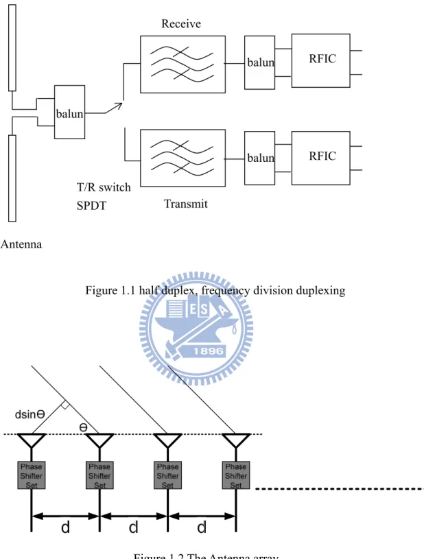
More and more microwave system and mm-wave RFICs are constructed by balanced circuit no meter the CMOS or GaAs RFICs. So the requirements for balanced passive device increase day by day. Baluns are used to transfer the single-ended signal to the balanced signal. Conventionally, a single ended signal is transformed to a balanced signal to feed to the input of a RFIC or transformed the balanced signal back from the output of a RFIC to a single ended signal. The Figure 1.1 shows the half duplex, frequency division duplexing transmitter. Because the IC and antenna are balanced, it costs two balun transformers to transfer the signal mode to achieve the system requirement. The complicated procedure can be simplified by the balanced passive circuit.
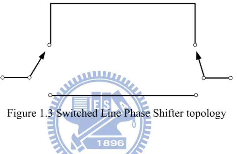
Especially for the military application, balanced digital phase shifter is an essential part the phase array antenna. For example, ESA radar (Electronically Scanned Array radar) changing the beam direction by adjusting the phase of antenna element to avoid mechanical motor driving. Not like mechanical radar, there are many advances in this kind of phase array radar. High sweeping speed, high mobility of changing the beam direction, high accuracy, and no machinery breakdown bring many advantages. Figure1.1
2
shows an antenna array containing the phase shifter sets.
Figure 1.1 half duplex, frequency division duplexing
Figure 1.2 The Antenna array
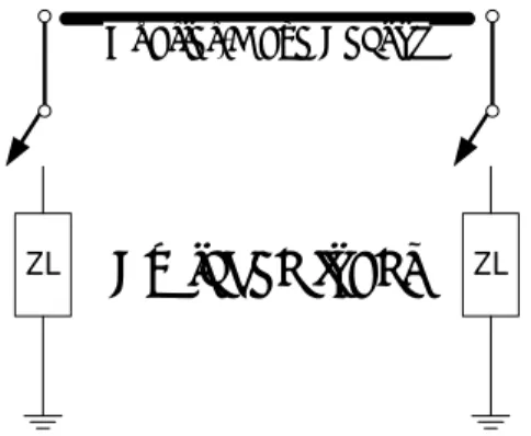
There are many kinds of phase shifters. The switched path circuit is shown in Figure1.3. The short arm is reference arm, and the long arm is the delay arm. Different electrical length can be made by passing difference arm length. The phase changing can
balun balun balun RFIC RFIC Antenna T/R switch SPDT Transmit Receive
3
be achieved by providing different transmission path. It is very important to choose a frequency band for this phase shifter. Because we use the PIN diode switches in 18GHz for “chip-and wire” construction. Up into millimeterwaves, in MMIC design, it often realized with FETs. FETs can overcome their off-state capacitance by using a shunt inductor trick at very high frequencies. The diodes are almost never used in monolithically. It is a big problem for the variation in wirebond inductance associated with MIC construction, and the frequency is limited, too.
Figure 1.3 Switched Line Phase Shifter topology
The main concept used in this thesis is developed from the loaded-line phase shifters shown in Fig1.4. This type of phase shifters are often used for the angle of 45 degree or lower than 45 degree. The loads ZL are the same, so the perturbation in the phase of the signal is created when switched into the circuit. The effect on the amplitude of the signal are very small. To let the loss of phase shifter minimize, the loads chosen should have very high reflection coefficient. The quarter-wave section loaded with two same loads can minimize and equalize the amplitude perturbation in both states. The phase versus
frequency response of loaded line phase shifter is much flatter than the switched line phase shifter.
4
Quarter-Wave Section
ZL
Switched loads
ZLFigure 1.4 Loaded-line phase shifter
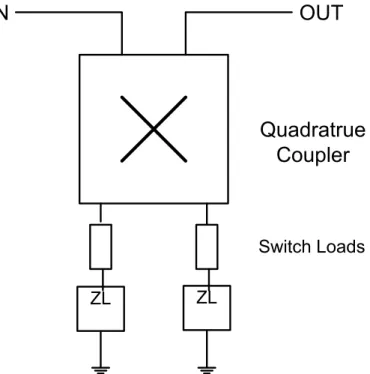
Here is another type of phase shifter, called reflection type phase shifter, shown in Fig. 1.5. The input signal into two signals 90 degrees out of phase are divided by an equal-split quadrature coupler. When the loads are identical in reflection coefficient, these signals, which reflect from a pair of switched loads, combine in phase at the phase shifter output. It is not like the loaded line structure, the quadrature phase shifter can be used to provide any desired phase shift. When the condition is ideal, the loads present purely reactive impedances. These can be presented by a short circuit to an open circuit, or anything in between. The bandwidth of this structure depends on the bandwidth of the quadrature coupler. The frequency band of operation is strongly influenced by the size of a
quadrature phase shifter constructed by one or more quarter-wave sections. Because the loads can be biased simultaneously, only one control signal is required for a quadrature phase shifter.
5
IN
OUT
Quadratrue
Coupler
Switch Loads ZL ZLFigure 1.5 Reflection phase shifter
The advantage of the balanced circuit can be connected by the phase inverter to form a digital phase shifter, these design use the property of symmetric circuit. The even mode and the odd mode correspond to open circuit and short circuit. The advantage of this design is the accuracy and structurally simple. In the past, we need the exact model for diode to design a low error phase shifter. And the balanced phase shifter can be directly link to the balanced antenna. It is very useful for us to design the phase array antenna.
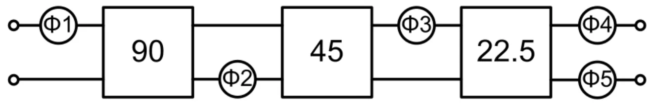
Figure 1.2 is the proposed balanced 4-bit phase shifter set. The five Φ devices between the 90, 45, 22.5 phase shifters are the 180 degree phase shifters for switching operating mode of the 90, 45, 22.5 degree balanced phase shifters. For example, if we want a 112.5(180x0+90x1+45x0+22.5x1) degree phase shift, assuming the “1” means to activate the 180 degree phase shift device, and “0” means to deactivate it. The 5 digits should be set to 01110. After we set the four 180 degree phase shift devices to 01110, the signal mode will be odd, even, odd, and odd in order.
6
Φ1
Φ2
Φ3
Φ5
Φ4
Figure 1.6 The 4-bit phase shift set
In this way, we can know that performance is better while the number of digit increasing, the n’th phase shift is
2 360 n o = Δφ (1.1)
From Eq. 1.1, increasing of n will decreasing the phase shift, and the realization will be more difficult (because of the smaller allowed phase error), For example the truth table for n=2 (Figure 1.3) is shown in Table 1.1,
Figure 1.7
3bit balanced digital phase shifter 90
Φ Φ Φ
Φ 45
phaser #1 phaser #2 phaser #3
phaser #4 Balanced
input signal
Balanced output signal
7
Phase state
Phaser#1 Phaser#2 Phaser#3 Phaser#4 90 45
0,360 1 1 1 1 Odd Odd 45 1 0 0 1 Odd Even 90 0 0 1 1 Even Odd 135 0 1 0 1 Even Even 180 1 1 0 0 Odd Odd 225 1 0 1 0 Odd Even 270 0 0 0 0 Even Odd 315 0 1 1 0 Even Even Table 1.1
8
Chapter 2
Basic Theory
2.1 Analysis and Characteristics of the
LoadedLine Phase Shifter [1]
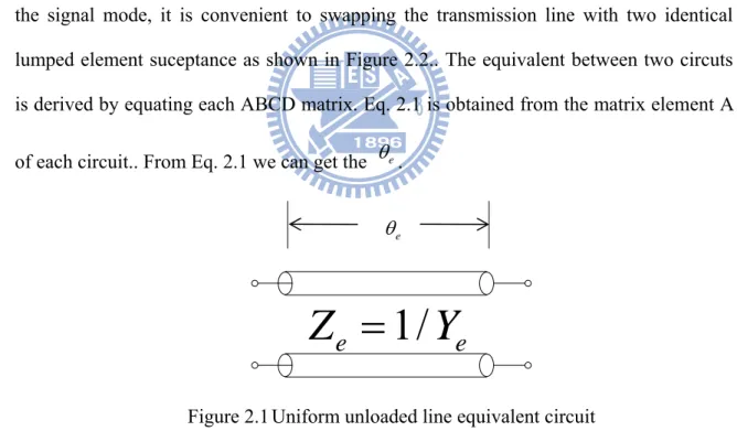
Each phase shifter of the phase shift set is original from a simple uniform length of transmission line shown in Figure 2.1. While we want to change the phase by switching the signal mode, it is convenient to swapping the transmission line with two identical lumped element suceptance as shown in Figure 2.2.. The equivalent between two circuts is derived by equating each ABCD matrix. Eq. 2.1 is obtained from the matrix element A of each circuit.. From Eq. 2.1 we can get the θe.
1/
e
e
Z
=
Y
e
θ
Figure 2.1 Uniform unloaded line equivalent circuit
θ
9
0
cosθe =cosθ −BZ sinθ (2.1) After this, we equate the ratio of matrix elements B and C, B/C, of each circuit,. We can obtain an expression for Y of the uniform line. E
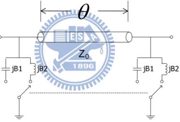
1/ 2 2 0 1 ( 0) 2 0cot E Y =Y ⎡⎣ − BZ + BZ θ⎤⎦ (2.2) We can use Eq. 2.1 to get the phase shift. The Eq. 2.2 is for the matching condition. This mismatch is influenced by the suceptance. To meet the matching condition for both states, the absolute value of shunt loaded suceptance in two states must be the same and the origional line length should be 90˚.For the phase shift we are interested in, let us consider a switched suceptance loaded-line phase shifter as shown in Figure 2.3.
θ
Figure 2.3 Switched Transmission Phase Shifter Section
First, we want to let the θ =90˚, B1=+j0.2, and B2=-j0.2. When θ =90˚ , cosθ =0; When the switches is selected to state 1, cosθE equals -0.2. On the other hand, the
switches select state 2, cosθE is +0.2. The electrical length QE for state 1 is 90o-P1 and
for state 2 is 90o+P2.
10
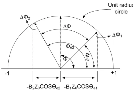
length difference of the loaded-line circuit for these two conditions.
Figure 2.4 Graphical representation of transmission phase shifter phase length change
The electrical length of this line whose θ = 90˚ is shown by the vector with origin at the center of the unit radius circle.
Clockwise from the horizontal axis, this vector has an angle of 90˚ measured. When the transmission line which is 90˚ length is loaded by a pair of shunt inductive susceptances, the cosine of its angle is negative is shown by the Eq. 2.1. Base on this fact we can know that the total electrical length, θE2, must be somewhat longer than 90˚
because its projection onto the horizontal axis is negative. So it falls to the left of the vertical, 90˚vector. From Eq. 2.1 the length of this projection is −B Z2 0.
In the same way, when the line length is loaded capacitively, the cosine of its equivalent electrical length is positive, and the net electrical length is less than 90˚. It is shown for the vector with angle θE1. The phase shift presented by φΔ is equal to the
11
difference in the equivalent electrical lengths ( φΔ = θE2 - θE1). We can see from the
present example, the values for θE1 is 101.6˚. And θE2 is 78.5˚, respectively. This
provides a net phase shift of 23˚.
From Figure 2.4, we can see that, the sum of the individual phase phase shifts, Δφ1
and Δφ2 become the total phase shift, φΔ . These phase shifts represent the
perturbations of the original 90˚ line length. The perturbations are introduced alternately by the pair of capacitors, B1, and the pair of inductors, B2. From Figure 2.4 it can be seen that φ Δ = Δφ1 + Δφ2 (2.3) 1 1 0 sin(Δφ) B Z= (2.4) 2 2 0 sin(Δφ ) B Z= (2.5) If the condition, 1 φ
Δ and Δ << 90˚φ2 Δ ≈ φ1 B Z and 1 0 Δ ≈ φ2 B Z , hold, 2 0
We can know the total phase shift from
2 1 0
(B B Z) φ
Δ = − (2.6)
When B Z1 0 ≠B Z2 0(provided both B Z and 1 0 B Z are much less than unity) and 2 0
even when θ ≠90˚(provide it is within +20, -20 of 90˚), we can applies this approximate expression for phase shift. It is therefore, for designing loaded-line phase shifter sections, the expression is very useful. A literal statement of this result is that for a quarter wave spaced pair of symmetrically switched susceptances, the phase shift produced is numerically equal in radians to the difference in normalized susceptance switched by one
12
of them.
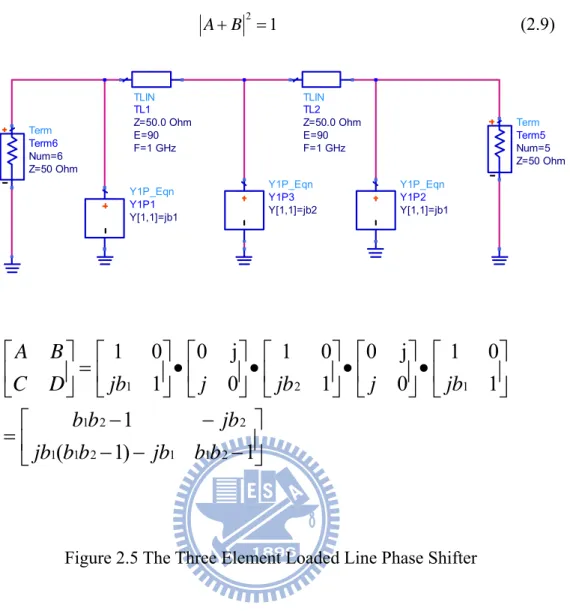
2.2 Three Element Loaded Line [1]
In chapter 2.1, 45˚ phase shift is the largest degree for the two element loaded line circuit just described; if we need the 90˚ degree phase shift, two such sections would be needed . Since both sections are switched together the overall equivalent circuit appears as a three element loaded line phase shifter. It follows that if the center element susceptance is chosen to be somewhat different than twice the end element susceptance, some performance improvement may be possible. So we analytically use the three element transmission phase shifter for this reason.
Figure 3.1 describes the circuit to be analyzed. The term port (the generator), load, and the line impedances have been made unity; thus, the values b1b2 represent normalized
susceptances. As shown below, in this situation when the elements are spaced by a quarter wavelength, the circuit is analyzed. At the beginning a t the load end to obtain the resulting overall matrix representation, ABCD1,2 ,the five individual ABCD matrices are
shown along with the sequence of their multiplication. The complete five matrix multiplication can be performed easily using only the steps shown in Fig 2.4.
For the case, from the defining equations for the ABCD matrix, the load impedance is unity ( V2/ I2 = 1 ), it follows that
1 2 2
V =AV +BI
1 ( ) 2
V = A B V+ (2.7)
For the circuit is matched. when Ohmic dissipation is neglected. It is necessary that
1 2
V =V = + (2.8) A B
13 2 1 A+B = (2.9) Term Term5 Z=50 Ohm Num=5 Term Term6 Z=50 Ohm Num=6 Y1P_Eqn Y1P2 Y[1,1]=jb1 Y1P_Eqn Y1P1 Y[1,1]=jb1 TLIN TL1 F=1 GHz E=90 Z=50.0 Ohm TLIN TL2 F=1 GHz E=90 Z=50.0 Ohm Y1P_Eqn Y1P3 Y[1,1]=jb2
Figure 2.5 The Three Element Loaded Line Phase Shifter
We substitute the values for A and B. Then take is into Eq. 2.9. For a transmission match condition 1 2 2 1 2 1 b b b = + (2.10)
Since the denominator is always positive, we can know that b1 and b2 must have the
same sign. Thus, both susceptances must have the same sign. Both susceptances must be either capacitive or inductive.
When the input is matched, the input voltage, V1, and the generator voltage, 2V0,
have the same phase and the transmission phase, ψ, of the network is given by
⎥
⎦
⎤
⎢
⎣
⎡
−
−
−
−
−
=
⎥
⎦
⎤
⎢
⎣
⎡
•
⎥
⎦
⎤
⎢
⎣
⎡
•
⎥
⎦
⎤
⎢
⎣
⎡
•
⎥
⎦
⎤
⎢
⎣
⎡
•
⎥
⎦
⎤
⎢
⎣
⎡
=
⎥
⎦
⎤
⎢
⎣
⎡
1
)
1
(
1
1
0
1
0
j
0
1
0
1
0
j
0
1
0
1
2 1 1 2 1 1 2 2 1 1 2 1b
b
jb
b
b
jb
jb
b
b
jb
j
jb
j
jb
D
C
B
A
14 2 2 0 1 arg( ) arg( )V V V V φ = = arg(A B) = − + (2.11)
The three element loaded line phase shifter is under the matching condition.
1 2 1 2 tan ( ) 1 b b b φ = − − − (2.12)
Substituting the value for b2 from Eq. 2.10, then we can get the phase shift,
1 1 2 1 2 tan ( ) 1 b b φ = − − (2.13)
The basic electrical length of the network is -180˚. The length is corresponding to the phase delay of the two 90˚ line sections. b1 and b2, as the susceptances, help perturb this
length; if they are made switchable, perturbations of the half wavelength of line. For example, if b1=+1, from equation (2.10), it follows that, for a match, b2=+1 as well, and
1
(b 1) 270
φ = = + = − ° (2.14)
To switch all susceptances between +1 and -1, we can be obtained
1 1
(b 1) (b 1) 180
φ φ φ °
15
2.3 Richard’s Transformation [2]
In order to meet the –jb and +jb condition, The circuit will be adjusted to two different modes without the switching object, we need to use the inductors and capacitors of a lumped-circuited filter design can be replaced with short-circuited and open-circuited stubs, as shown in Figure.2.4.
(a)
(b)
Figure 2.6 Richard’s transformation. (a) For an inductor to a short-circuited stub. (b) For a capacitor to an open-circuited stub
The reactance of an inductor and the susceptance of a capacitor are jXL and jBC. We
want to maps the ω plane to the Ω plane, which repeats with a period of ω υl/ P =2π.
Thus, the LC network can be synthesized by open-end short-circuited transmission lines. This transformation was introduced by P.Richard.
tan
L
16
tan
C
jB = Ω =j C jC βl (2.17)
These results indicate that an inductor can be replaced with a short-circuited stub of length βl and characteristic impedance L, while a capacitor can be replaced with an open-circuited stub of length βl and characteristic impedance 1/C. Unity filter impedance is assumed.
For a low-pass filter prototype, cutoff occurs at unity frequency; we can obtain the same cutoff frequency for the Richard’s-transformed filter, the equation
tan tan( ) P ω β υ Ω = l= l (2.18) Shows that 1 tanβ Ω = = l (2.19) Ω C = 1
Which gives a stub length of l=λ/ 8, where λ is the wavelength of the line at the cutoff frequency, ωC . At the frequency ω0 = 2ωC, the lines will be / 4λ long, and an
attenuation pole will occur. At frequencies away from ωC , the impedances of the stubs
will no longer match the original lumped-element impedances, and the filter response will differ from the desired prototype response. Also, the response will be periodic in frequency, repeating every 3ωC.
In principle, then the inductors and capacitors of a lumped-element filter design can ve replaced with short-circuited and open-circuited stubs, as illustrated in FigureX. Since the lengths of all the stubs are the same( / 8λ at ωC), these lines are called commensurate
17
2.3 The quarterwave transformer [2]
The quarter-wave transmission line is a useful circuit for impedance matching. A transmission line of impedance Z1 and electrical length θ terminated in load impedance RL is shown in Fig. 2.7 The input impedance Zin can be found as
θ θ tan tan 1 1 1 L L in jR Z jZ R Z Z + + = (2.29)
When the transmission line equals to quarter-wave, the electrical length θ equals to π/2. By taking the limit of (2.29) as θ → π/2, we can get (2.30) from (2.29)
L in R Z Z 2 1 = (2.30)
Z
1θ
Z
inR
LZ
0Fig. 2.7 A transmission line terminated in load impedance RL
From (2.30), when there is a load of impedance RL, and we want to match it to the port of impedance Z0 with the reflection coefficient Γ to be zero, the characteristic impedance Z1 of the quarter-wave transmission line should be chosen as
L
R Z
Z1 = 0 (2.31)
However, the quarter-wave transformer is designed at some specific frequency f0, the reflection coefficient Γ will not be zero near the design frequency f0. When using the
18
quarter-wave transformer for impedance matching, we may care about the bandwidth of the quarter-wave transformer.
As shown in Fig. 2.8, when the quarter-wave transformer is operated near its design frequency, the reflection coefficient magnitude will increase. Thus, for the reflection coefficient level Γm, we can calculate the fractional bandwidth BW as follow [2]
⎥ ⎥ ⎦ ⎤ ⎢ ⎢ ⎣ ⎡ − Γ − Γ − = Δ = − 0 0 2 1 0 2 1 cos 4 2 Z R R Z f f BW L L m m π (2.32) m
Γ
Γ
2
π
θ
19
Chapter3
The proposed phase shifter
Three phase shifters are designed for shifting 90, 45, 22.5 degree respectively. The design procedures will be presented and so are the simulation results and measurement results. In addition, the simulation tool is ADS from Agilent and the EM simulation is Sonnet. All the measurements are obtained by four-port network analyzer E5070. All the phase shifters are fabricated on Rogers RO4003 with a relative dielectric constant of 3.38 and thickness of 20 mil.
3.1 Design procedure and Realization for
90 degree phase shifter
Term Term10 Z=25 Ohm Num=10 Term Term11 Z=25 Ohm Num=11 Term Term12 Z=100 Ohm Num=12 TF3 TF4 T2=2.00 T1=2.00 1 2 3 3 1 -T1 1 -T2 1 TLIN G16 F=2.5 GHz E=90 Z=Z Ohm TLIN G21 F=2.5 GHz E=90 Z=Z Ohm TLIN TL3 F=2.5 GHz E=X Z=Y Ohm TLIN TL5 F=2.5 GHz E=B Z=A Ohm TLIN TL4 F=2.5 GHz E=X Z=Y Ohm TF3 TF3 T2=2.00 T1=2.00 1 2 3 3 1 -T1 1 -T2 1 Term Term9 Z=100 Ohm Num=9 TLIN TL2 F=2.5 GHz E=X Z=Y Ohm VAR VAR5 B=45 {t} EqnVar VAR VAR3 Z=49.155 {t} Eqn Var VAR VAR1 X=45 {t} Eqn Var VAR VAR4 A=72.64 {t} EqnVar VAR VAR2 Y=119 {t} Eqn Var TLIN G20 F=2.5 GHz E=90 Z=Z Ohm TLIN G15 F=2.5 GHz E=90 Z=Z Ohm TLIN TL1 F=2.5 GHz E=X Z=Y Ohm TLIN TL6 F=2.5 GHz E=B Z=A Ohm S_Param SP1 Step=0.01 GHz Stop=3.0 GHz Start=2.0 GHz S-PARAMETERS (a)
20
(b)
(c)
Figure 3.1 The overall circuit diagram. (a) In circuit simulation tool, ADS. (b, c) In EM simulation tool, Sonnet.
A Y Z X B 72.64Ω 119Ω 49.155Ω 45˚ 45˚
21
W1 W2 W3 W4 7 23 46 44 W5 L1 L2 L3
16 1406 722 60
Table. 3.2 Physical dimensions of the proposed 90 degree phase shifter. (Unit: mil)
At first, the center frequency is set to 2.5GHz, the deeps of the two mode’s S21 parameters should be at 2.5GHz at the same time. Under the consideration of the bandwidth, we adjust the resistance a little bit. So the pass-band is from 2.2G to 2.8G. And the phase error is about -2.5 (center frequency) to +2.5 (2.2GHz). That is about 2.7%. These simulation results are shown below.
simulation S parameter for 90 degree phase shifter
frequency:Hz
1.8e+9 2.0e+9 2.2e+9 2.4e+9 2.6e+9 2.8e+9 3.0e+9 3.2e+9
S( db ) -70 -60 -50 -40 -30 -20 -10 0 10 OddmodeS11 OddmodeS21 EvenmodeS11 EvenmodeS21
22
simulation phase response for 90 degree phase shifter
frequency:Hz
1.8e+9 2.0e+9 2.2e+9 2.4e+9 2.6e+9 2.8e+9 3.0e+9 3.2e+9
phase error : dre gee -4 -2 0 2 4 6 8 10 12
phase error vs frequency
Figure 3.3 Sonnet Simulation: phase error for 90 degree phase shifter
23
S parameter for 90 degree phase shifter
frequency:Hz
0 1e+9 2e+9 3e+9 4e+9 5e+9 6e+9
S( db ) -50 -40 -30 -20 -10 0 Evenmode S11 Evenmode S21 Oddmode S11 Oddmode S21 (a)
phase response for 90 degree phase shifter
frequency:Hz
1.8e+9 2.0e+9 2.2e+9 2.4e+9 2.6e+9 2.8e+9 3.0e+9 3.2e+9
ph ase er ror : dr egee -8 -6 -4 -2 0 2 4 6 8 10
phase error vs frequency
24
(b)
Figure 3.5 Simulation result (a) S parameter for 90 degree phase shifter (b) phase response for 90 degree phase shifter
Figure 3.5 show the results of the implementation. The center frequency is about 2.5GHz, and the S parameter is close to the simulation results. The phase error is between -0.5 (2.2GHz) to +5.5 (2.6GHz). The max error rate is about 6.1%.
25
3.2 Design procedure and Realization for
45 degree phase shifter
S_Param SP1 Step=0.01 GHz Stop=3.0 GHz Start=2.0 GHz S-PARAMETERS Term Term6 Z=25 Ohm Num=6 Term Term5 Z=100 Ohm Num=5 TF3 TF1 T2=2.00 T1=2.00 1 2 3 3 1 -T1 1 -T2 1 TLIN TL7 F=2.5 GHz E=X Z=Y TLIN TL5 F=2.5 GHz E=X Z=Y Term Term8 Z=25 Ohm Num=8 TF3 TF2 T2=2.00 T1=2.00 1 2 3 3 1 -T1 1 -T2 1 Term Term7 Z=100 Ohm Num=7 TLIN TL6 F=2.5 GHz E=X Z=Y TLIN G21 F=2.5 GHz E=B Z=Z TLIN G20 F=2.5 GHz E=B Z=Z TLIN TL8 F=2.5 GHz E=X Z=Y (a) (b)
26
Figure 3.6 The overall circuit diagram. (a) In circuit simulation tool, ADS. (b) In EM simulation tool, Sonnet
Y Z B X 119Ω 49.155Ω 90˚ 45˚
Table. 3.3 Resistance and the Electrical length of the proposed 45 degree phase shifter.
W1 W2 W3 L1 L2 L3
7 53 44 697 744 60
Table. 3.4 Physical dimensions of the proposed 90 degree phase shifter. (Unit: mil)
The simulation results below show that the pass-band is from 2.1GHz to 2.85GHz, and the phase error is about 2.2% (-1 to +1).
simulation S parameter for 45 degree phase shifter
frequency:Hz
1.8e+9 2.0e+9 2.2e+9 2.4e+9 2.6e+9 2.8e+9 3.0e+9 3.2e+9
S( db) -70 -60 -50 -40 -30 -20 -10 0 10 Oddmode S11 Oddmode S21 Evenmode S21 Evenmode S11
27
simulation phase response for 45 degree phase shifter
frequency:Hz
1.8e+9 2.0e+9 2.2e+9 2.4e+9 2.6e+9 2.8e+9 3.0e+9 3.2e+9
phase error : dre gee -2 0 2 4 6
phase error vs frequency
Figure 3.8 Sonnet Simulation: phase error for 45 degree phase shifter
28
S parameter for 45 degree phase shifter
frequency:Hz
1.8e+9 2.0e+9 2.2e+9 2.4e+9 2.6e+9 2.8e+9 3.0e+9 3.2e+9
S(db) -60 -50 -40 -30 -20 -10 0 Evenmode S11 Evenmode S21 Oddmode S11 Oddmode S21 (a)
phase response for 45 degree phase shifter
frequency:Hz
1.8e+9 2.0e+9 2.2e+9 2.4e+9 2.6e+9 2.8e+9 3.0e+9 3.2e+9
pha se error : dregee -6 -4 -2 0 2 4 6 8
phase error vs frequency
29
Figure 3.10 Simulation result (a) S parameter for 45 degree phase shifter (b) phase response for 45 degree phase shifter
Figure 4.10 show the results of the implementation. The center frequency is about 2.6GHz, and the S parameter is not as good as the simulation results. The bandwidth is narrower. The phase error is between -5 (2.8GHz) to +1 (2.2GHz). The max error rate is about 11%
3.3 Design procedure and Realization for
22.5 degree phase shifter
VAR VAR5 n=2 Eqn Var Term Term7 Z=100 Ohm Num=7 Term Term8 Z=25 Ohm Num=8 Term Term6 Z=25 Ohm Num=6 Term Term5 Z=100 Ohm Num=5 TF3 TF1 T2=n T1=n 1 2 3 3 1 -T1 1-T2 1 TF3 TF2 T2=n T1=n 1 2 3 3 1 -T1 1 -T2 1 TLIN TL16 F=2.5 GHz E=D Z=X Ohm TLIN TL17 F=2.5 GHz E=D Z=X Ohm TLIN TL18 F=2.5 GHz E=90 Z=H Ohm TLIN TL19 F=2.5 GHz E=90 Z=H Ohm TLIN TL20 F=2.5 GHz E=90 Z=Y Ohm TLIN TL15 F=2.5 GHz E=90 Z=Y Ohm TLIN TL14 F=2.5 GHz E=90 Z=H Ohm TLIN TL13 F=2.5 GHz E=90 Z=H Ohm TLIN TL12 F=2.5 GHz E=D Z=X Ohm TLIN TL11 F=2.5 GHz E=D Z=X Ohm (a)
30
(b)
Figure 3.11 The overall circuit diagram. (a) In circuit simulation tool, ADS. (b) In EM simulation tool, Sonnet
H X Y D 33.8245Ω 119Ω 23.18Ω 45˚
Table. 3.5 Resistance and the Electrical length of the proposed 22.5 degree phase shifter.
W1 W2 W3 L1 L2 L3 80 7 131 682 673 757
31
Figure 3.12 Photograph of 45 degree phase shifter
simulation S parameter for 22.5 degree phase shifter
frequency:Hz
1.8e+9 2.0e+9 2.2e+9 2.4e+9 2.6e+9 2.8e+9 3.0e+9 3.2e+9
S(db) -80 -60 -40 -20 0 20 Evenmode S21 Evenmode S11 Oddmode S21 Oddmode S1
32
simulation phase response for 22.5 degree phase shifter
frequency:Hz
1.8e+9 2.0e+9 2.2e+9 2.4e+9 2.6e+9 2.8e+9 3.0e+9 3.2e+9
pha se error : dre gee -0.4 -0.2 0.0 0.2 0.4
phase error vs frequency
Figure 3.14 Sonnet Simulation: phase error for 22.5 degree phase shifter S parameter for 22.5 degree phase shifter
frequency:Hz
1.8e+9 2.0e+9 2.2e+9 2.4e+9 2.6e+9 2.8e+9 3.0e+9 3.2e+9
S(db) -35 -30 -25 -20 -15 -10 -5 0 Evenmode s11 Oddmode s11 Evenmode s21 Oddmode s11 (a)
33
phase response for 22.5 degree phase shifter
frequency:Hz
1.8e+9 2.0e+9 2.2e+9 2.4e+9 2.6e+9 2.8e+9 3.0e+9 3.2e+9
phase error : dre gee 0.6 0.7 0.8 0.9 1.0 1.1
phase error vs frequency
(b)
Figure 3.15 Simulation result (a) S parameter for 22.5 degree phase shifter (b) phase response for 22.5 degree phase shifter
Figure 4.10 show the results of the implementation. The center frequency is about 2.6GHz, and the S parameter is not as good as the simulation results. The bandwidth is narrower. The phase error is between 0.65 (2.6GHz) to +1 (2.3GHz). The max error rate is about 4.44%
34
Chapter 4
Conclusion
The balanced digital phase shifter has many advantages,
1. The susceptance of the load is exactly equal to the characteristic admittance of the transmission line. Thus we can easily improve the accuracy.
2. Requirement for the susceptance of the load can be precisely achieved. 3. The diode can be used repeated only for 0/180 phase shift.
4. The phase shifter can be directly link to the balanced antenna or circuit because of the balanced characteristic.
35
References
[1] D. M. Pozar, Microwave Engineering, 2nd ed. New York: Wiley, 1998. [2] Joseph F. White, Semiconductor Control, Dedham, Mass: Artech, 1977, ch. IX