國 立 交 通 大 學
電子工程學系電子研究所
碩士論文
對製程中引發應力之 P-型通道金氧半電晶體的
1/f 雜訊研究
A Study of Low Frequency Noise in process
Induced Stress PMOSFETs
研究生:陳又正
對製程中引發應力之 P-型通道金氧半電晶體的
1/f 雜訊研究
A Study of Low Frequency Noise in process
Induced Stress PMOSFETs
研究生:陳又正
Student: Yu-Cheng Chen
指導教授:陳明哲 博士 Advisor: Dr. Ming-Jer Chen
國 立 交 通 大 學
電子工程學系 電子研究所
碩士論文
A Thesis
Submitted to Department of Electronics Engineering & Institute of Electronics
College of Electrical and Computer Engineering National Chiao Tung University
In partial Fulfillment of the requirements For the Degree of Master
In
Electronic Engineering October 2009
Hsinchu, Taiwan, Republic of China
中華民國九十八年十月
A Study of Low Frequency Noise in process
Induced Stress PMOSFETs
Student: Yu-Cheng Chen
Advisor: Dr. Ming-Jer Chen
Institute of Electronics
National Chiao-Tung University
Abstract
For 1.27nm thick gate oxide p-channel MOSFETs , the hole mobility booster by the means of process strained silicon (PPS) technique is applied. With the noise measurement, we can extract the trap density Nt and scattering factor α in STI compressive stress PMOSFETs. Specially, We characterize the 1/f noise power spectra density (PSD) of the drain current both in the channel width (W) and the channel length direction. In the channel length direction, the experiment results show that the STI induced stress can provide more interface trap density. However, in the channel width direction, the main decrease of the average trap density comes from the edge structure. The I-V measurement can also give us that the information the stress on narrow device is not the only reason for
對製程中引發應力之 P-型通道金氧半電晶體的
1/f 雜訊研究
研究生:陳又正
指導教授:陳明哲博士
國立交通大學
電子工程學系電子研究所
摘要
對於 1.27 奈米厚閘極之 p 型通導金氧半電晶體,可應用製程引 發應力提升電洞的遷移率。由雜訊量測,我們可以得到淺溝槽絕緣引 發應力下 p 型通導金氧半電晶體之缺陷密度及散射系數。我們可以由 汲極電流得到通道寬和通道長方向的 1/f 雜訊頻譜。在通道長方向, 實驗結果顯示淺溝槽絕緣引發應力會導致更多的缺陷。然而,在通導 寬方向,缺陷密度的降低主要來自邊緣結構的不同。同時,電性量測 也可以告訴我們,應力並不是在通道寬方向唯一造成電洞的遷移率變 化的原因。對雜訊和電性的量測實驗而言,反向窄通道效應(INCE) 應是適合的解釋。誌 謝
首先,要感謝的是我的指導教授陳明哲博士,在研究上給我啟發; 感謝我的博士班學長們,給這篇論文的靈魂;感謝我的同學們,多少 個的深夜裡一起苦思解決之道;感謝幫助我量測的學弟們,感謝你們 的付出;感謝我的家人,這二年的無私的支持。回首二年研究所生活, 得之於人者太多,出之於己者太少,感謝幫助過我的人,更感謝給我 挫折的人,因為你們我才能了解做真理,讓我的心靈更加豐足,成功 帶來榮耀,失敗則是最好的導師,是你們讓我成為堅強的男子漢。 2009/10/4 又正寫於深夜宜蘭家中Contents
Abstract (English)……….(i) Abstract (Chinese)………(ii) Acknowledgement……….(iii) Contents………...………..(iv) List of Caption………(v)Chapter 1 Introduction……….1
Chapter 2 Low Frequency Noise……….3
2.1 MOSFET Fundamentals
-Current-Voltage Relations….3
2.2 Noise and fluctuation...6
2.2.1 The McWorther model (Number fluctuation)…...6
2.2.2 The Hooge model (Mobility Fluctuation)………..10
2.2.3The Unified model (Number Fluctuation with Mobility Correlation)……….12
Chapter 3 Experimental Setup………..14
3.1 Introduction………..14
3.2 Device Structure Description………..14
Chapter4 Experimental Results and Detail
Analysis………16
4.1 Noise Fitting Between (Vg-Vth) and Id/gm…….….16
4.2 Stress Simulation by Sentaurus TCAD Simulation
and Mobility-Shift Extract Stress……….18
4.3 TEM Picture……….…20
4.4 Channel Length Direction related IV and Noise
Experiment……….21
4.4.1 Vth and Mobility Shift………..21
4.4.2 Noise Data Analysis………..21
4.5 Channel Width Direction related IV and Noise
Experiment ………22
4.5.1 Vth and Mobility shift………...22
4.5.2 Noise Data Analysis………..23
List of Captions
Fig.1 the Energy band diagram illustration of a PMOSFET biased near the threshold point………28 Fig.2 A schematic description of the charge distribution in the MOS structure……….29 Fig.3The schematic illustration of oxide traps exchange with the channel carriers causing a fluctuation in the surface potential………30 Fig4The band diagram describe the tunneling transitions, (i) directly [7] or (ii) using interface traps as stepping stones [8] from the Si to gate oxide………31 Fig.5 The STI structure induced stress in channel width (W) and channel length direction (L)………32 Fig.6The difference between id/gm and Vg-Vth fitting method. We can see that Vg-Vth is a straight line, instead id/gm is a curve ………33 Fig.7 Two different fitting method (Vg-Vth, Id/gm) on the same sample………..34 Fig.8 The contours of stress distribution across the whole device……...35 Fig.9 The stress distribution along the channel width………36 Fig.10 Comparing our simulation result with Shih[18]………37 Fig11 The separated stress in terms of the average edge stress and average flat region stress………..38 Table.1 The Measured long p- and n-channel MOSFET piezoresistance coefficients for (001) and (110) wafers compared to bulk Si piezoresistance [15]………39
Fig.12 The Vth shfit due to gate to STI spacing (A) induced stress. ….40 Fig.13 The mobility shift due to gate to STI spacing (A) induced stress……….41 Fig .14 measured Svg0.5 varies Id/g at 25Hz with spacing A=10um……42 Fig .15 measured Svg0.5 varies Id/g at 25Hz with spacing A=2.4um…43 Fig .16measured Svg0.5 varies Id/g at 25Hz with spacing A=0.495um…44 Fig .17 measured Svg0.5 varies Id/g at 25Hz with spacing A=0.21um...45 Fig.18 The fittings used line for extracting the trap density Nt (cm-3eV-1) and scattering factor α (Vs/C)………46 Fig.19(a) The trap density Nt(cm-3eV-1). (b) the scattering factor α variation. Varies gate to STI Spacing………47 Fig 20 The Vth shift in narrow device, at L=1um,W=10,1,0.6,0.24, and 0.11um……….….48 F i g . 2 1 a T he mo b i l i t y va r ie s ga t e vo l t a ge o f f i v e d e v ic e (W=10,1,0.6,0.24,0,11um), L=1um………49 Fig.21b The anormal mobility shift in narrow devices………49
Fig 22a measured Svg0.5 varies Id/gm at 25Hz with W=10um……..50 Fig 22b The fitting line at 25Hz with W=10um……….50 Fig 23a measured Svg0.5 varies Id/gm line at 25Hz with W=1um……51 Fig 23b The fitting line at 25Hz with W=1um………..51
Fig 24b The fitting line at 25Hz with W=0.6um……….….…52 Fig 25a measured Svg0.5 varies Id/gm line at 25Hz with W=0.24um…53 Fig 25b The fitting line at 25Hz with W=0.24um……….53 Fig. 26a measured Svg0.5 varies Id/gm at 25Hz with W=0.11um…….…54 Fig. 26b The fitting line at 25Hz with W=0.11um……….54 Fig.27a The Trap density Nt variation in narrowing devices. ……….…55 Fig.27b The scattering factor α variation in narrowing devices………...55
Chapter 1 Introduction
Electronic devices exhibit random fluctuations in voltage (or current) at their terminals. These fluctuations are usually referred to as noise. It originates in the random, microscopic behavior of the charge carriers in the device. It is popular in detecting the inside part of electronic devices by low frequency noise. The non-destruction investigation is the most important feature of the noise measurement. There are four typical types of noise, random telegraph signal (RTS) or low frequency (1/f noise), thermal noise, and shot noise. Each one has its physical origin. In this research, We focus on the low frequency noise on the ultra-thin gate oxide PMOSFET with STI mechanical stress to investigate the stress effect on the channel carriers.
Channel strain engineering is currently recognized as an indispensable performance booster in producing next generation metal-oxide-semiconductor field-effect transistors (MOSFETs)[1]. In order to achieve this goal, two fundamentally different methods have been proposed :(I) Strained silicon(SSi) on a relaxed SiGe buffer layer and (II)Process strained silicon (PSS) through the trench isolation, silicide, and capping layer. The un-strain low-frequency noise has been extensively examined and it has provided many interface physics [2-3]. Thus, it is challenging to examine for low-frequency noise to find further
In the investigation of ultra-thin gate oxide MOSFET device undergoing, we conduct the compressive stress on two axis directions which provide us the different direction to determine the stress induced trap density in the process strained silicon (PPS). Meanwhile, we discuss the corner edge influence on mobility shift through I-V characteristic. The TEM picture and the TCAD stress simulation in the channel width direction are also prepared. Then combined with I-V Fitting, 1/f noise, we can capture a novel picture on the stress effect affects the trap density and the mobility scattering factor.
Chapter 2 Low Frequency Noise
2.1 MOSFET Fundamentals
Current-Voltage RelationsLet we first briefly review the fundamentals of MOSFET before describing the MOSFET noise sources in next subsection. The formation of the channel allows a large current to flow between source and drain as the device is switched on. In the inversion condition, the inversion charge density can be approximated as
)
(
)
(
eff gs th c iV
C
V
V
mV
Q
(2-1)Where Vc is the potential drop along the channel, Vth is the threshold
voltage, m is the body-effect coefficient, and Ceff =
ε
ox/tox is the gate oxide capacitance per unit area. The gate voltage controls the charge density in the channel, thereby modulating the conductivity between drain and source. The drain current depends on the conductivity and the applied electric field in the channel. The drain current can be derived in the linear region where VDS < VDS,sat, as]
2
/
)
[(
2ds ox eff DC
Vgs
Vth
Vds
mV
L
W
I
(2-2)where Nsub is the doping concentration in the substrate, Vfb the flat-band
voltage, εsi is the permittivity of Si and ΨB the energy difference
between the Fermi level Ef and the intrinsic level Ei. The plus signs in
Eq.(2-3) apply to NMOS and the minus signs to PMOS, respectively .
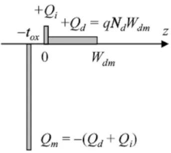
Fig.1 shows the energy band diagram of a PMOSFET biased near the threshold. Fig.2 is a schematic description of the charge distribution in the MOS structure. The flat-band voltage depends on the work function difference between the gate material and the substrate material and ψms
the equivalent (trapped or fixed ) oxide charge density at the oxide-silicon interface Qox ox ox ms fb
Q
C
V
/
(2-4)For N+ or P+ doped poly-Si gate and p-type or n-type Si substrate, the work function difference is calculated to be
)
/
ln(
/
56
.
0
sub i ms
kT
q
N
n
(2-5)where the plus or minus sign in front of the first term is for p-type or n-type gate material, respectively. For the second term, the plus sign applies for n-type substrate and the minus sign for p-type.
The factor
m
in Eqs.(2-1) and (2-2), called the body effect coefficient has been inserted to account for corrections to the simple theory. The value of m is typically between 1 and 1.4. It is calculated as follows [4]:The drain current in Eq. (2-2) increases with the drain voltage until a maximum is reached and saturation occurs. The drain voltage at saturation is
m
V
V
V
dV
dI
d/
ds
0
ds,sat
(
gs
th)
/
(2-6)
At this pinch-off point, the channel at the drain end vanishes. The electric field along the channel between the source end and the pinch-off point stays constant with increasing Vds> Vds,sat. By inserting Eq. (2-7) in Eq.
(2-2), the drain current in the saturation region can be written as
m
V
V
C
L
W
I
d eff ox gs th2
)
(
2
(2-7)
2.2 Noise and fluctuation
Metal-oxide-semiconductor field-effect transistor (MOSFETs) are finding more and more important applications in area of analog integrated circuits. There exist three models that have been invoked to account for the origin of flicker noise: Number fluctuation model, mobility
fluctuation model and unified correlated model.
2.2.1 The McWorther model (Number fluctuation)
In the number fluctuation model, as originally proposed by McWhorter [5], flicker noise is attributed to many discrete changes, called RTS noise, in drain current resulting from trapping and detrapping into single oxide defects in the oxide by tunneling. Fig.3 shows the schematic illustration of how the oxide traps exchange carriers with the channel, causing a fluctuation in the surface potential, giving the fluctuations in the inversion charge density. The g-r noise in the oxide charge generated by one trap that randomly captures and releases channel electrons can be written as
2 2 2 2 2 2 ) 2 ( 1 4 f Nox L W q C S SQox vgb ox (2-8)
The variance in △Nox due to a trap at energy E , Nox is the number of oxide charges can be calculated from the probability that the trap is occupied. The probability is given by Fermi-Dirac distribution function F(E)
1 ) ( , )] ( 1 [ ) ( kT E E Exp E f f n p (2-9) Then )) ( 1 )( ( )) ( 1 ( )) ( 0 ( ) ( )) ( 1 ( 2 2 2 E f E f E f E f E f E f Nox (2-10)
Now, the contribution from all traps in the gate oxide should be taken into account. The total PSD is found by summing over all traps whose noise contributions are given by Eq.(2-8). However, the individual traps are not known. It can instead assume a density of trap Nt (x,y,z,E) in volume and make an integration [6,7]
dxdydzdE
f
E
f
E
Ntf
L
W
q
S
Ec W L tox Ev Qox
0 2 0 0 2 2 2)
2
(
1
)
(
1
)(
(
4
(2-11)The product f(E)(1-f(E))=-kT (df(E)/dE )is sharply peaked around the quasi-Fermi level and Nt is considered as uniform over the gate area. Thus
dz
f
Nt
L
W
kT
q
S
Qox tox
0 2 2)
2
(
1
4
(2-12)where Nt is the density of traps in the gate dielectrics at the quasi-Fermi level (in unit of cm-3eV-1) since these traps are the only ones that contribute to the 1/f noise. Other traps are permanently filled or permanently empty. In the McWorther model, which assumes that trapping and detrapping occur through tunneling processes, the trapping time constant is given as
)
/
(
*
)
(
0
E
Exp
z
(2-13)For an electron tunneling from the interface (z = 0) to a trap located at a distance z in the gate oxide. The tunneling attenuation length λ is predicted by the Wentzel-Kramers-Brilloui (WKB) theory [7] to be
1 ] * 2 4 [ m B h
(2-14)where ΦB is the tunneling barrier height as seen by the carriers at the
interface and h is Planck’s constant. Calculations using Eq.(2-14) give A
1 ~
for the Si/SiO2 system. The time constant τ0 is often taken as
10-10 s. This yields z =2.6nm and 0.7nm for a frequency of 0.01Hz and 1MHz. Thus, oxide traps located too close to the channel interface are too fast to give 1/f noise, those located more than ~3nm from the interface are too slow to contribute. By inserting Eq. (2-13), the integral in (2-12) can be evaluated as ox r t vfb
WLC
f
N
kT
q
S
2 2
(2-15)The trap density can also vary with energy, which affects the bias and frequency dependence of the noise. The band diagram in Fig.4 describes the tunneling transitions, (i) directly [7] and (ii) using interface traps as stepping stones [8] from the Si to gate oxide, and the Window (z,E) of traps seen at a particular bias point (shaded area). The interface trap density often shows a U-shaped curve as a function of energy in the bandgap with increasing values towards the conduction of valence band edges. If the oxide trap density follows the same behaviour, Nt is predicted to increase with gate bias since the quasi-Fermi level approaches Ec to Ev. Due to the band bending of the gate oxide, an energy dependent trap density should be accompanied by a frequency exponent 1.Traps in the oxide interior are swept “faster” in energy than the traps at the channel interface. So, it is expected that 1and increases with gate bias in the case of a trap density that increases towards the band edges.
However, the tunneling model presented here is not the only one that can give the appropriate distribution of time constants in order to achieve the 1/f fluctuations. Another possibility is thermally activated traps with time constant exponentially depending on energy [9]:
]
/
[
,thExp
E
kT
o
(2-17)2.2.2 The Hooge model (Mobility Fluctuation)
On the other hand, the mobility fluctuation theory [10~12] considers the flicker noise as a result of the fluctuation in the bulk mobility based on the Hooge’s empirical relation for the spectral density of flicker noise in a homogenous sample.
The drain current noise generated by fluctuations in the channel carrier mobility is given according to Hooge’s empirical formula
i H d id
fWLQ
q
I
S
2 (2-18)In the linear region,Qi(V)Cox(VgsVthmV),Thus the normalized drain
current noise depends inversely on the gate voltage overdrive .The Hooge parameter can often be considered as a constant, but the channel position under the gate oxide and the bias dependence of different scattering mechanisms both likely affect the mobility fluctuation noise. The relation in Eq. (2-18) is only valid when the carrier density is uniform. In the saturation region, the carrier density varies parabolically along the channel and reaches zero at the drain end. Then the total channel drain current noise is evaluated by dividing the channel into small segments. Each generating a noise contribution and integrating over the channel, leading to
Vds d ds H d eff H eff L d H idI
fL
V
q
dV
I
W
fWL
q
dx
QidV
W
I
x
Qi
dx
fWL
q
Id
S
0 2 2 0 2 2{
/
}
)
(
(2-19)This equation is valid for all regions of operation, but VDS is replaced
with VDS,sat for VDS > VDS,sat. Using Vds,sat(VgsVth)/mand Eq.(2-7) the
following expression applies to the saturation range d ox ff H id
mI
C
WL
f
e
q
Id
S
3 22
(2-20) In the subthreshold region, the drain current is dominated by diffusiondx
x
dQi
q
WkT
I
d,diff
eff(
)
(2-21)Using the above expression in the integral to the left in Eq.(2-19),it is readiliy shown that the same final result can be obtained. However, the drain current and the total charge density Qi is independent of each other
for Vds>>kT/q. The mobility 1/f noise is also independent of Vds in this case and can be written as
Id
fL
KT
Id
S
id H e ff 2 22
(2-20)2.2.3
The Unified model (Number Fluctuation with Mobility Correlation)
A more widely accepted model, proposed by Hu’s group [6, 13], is based on a theory that incorporates both the oxide-trap-induced carrier number and surface mobility fluctuation mechanism. The flat band perturbation theory shows that fluctuating oxide charge density Qox is equivalent to a variation in the flat-band voltage
(2-21) The fluctuation in the drain current Id = f(V fb ,ueff) then yields[14]
(2-22)
Since d(Id)/d(Vfb)= -d(Id)/d(Vgs)=-gm , (+gm for PMOS) we have
ox ox eff eff d fb d
Q
Q
I
gmV
I
(2-23) ox ox fbQ
C
V
/
ox ox eff eff d fb fb d dQ
Q
I
V
V
I
I
One can define a coupling parameter or scattering parameter that reflects how a variation in the oxide charge couples to the mobility:
(2-24)
(valid for NMOS; a minus sign must be added for pMOS) Inserting in Eq(2-23) gives
(2-25)
Calculating the power spectral density PSD, we have
(2-26)
The first term in the parentheses of Eq.(2-26) is due to fluctuating number of inversion carriers and the second term to mobility fluctuation correlated to the number fluctuations. Note that α can be negative or positive depending on the increase or decrease mobility upon trapping a charge according to Eq.(2-24):
ox eff eff
Q
1
2 fb ox eff d fb m dg
V
I
C
V
I
2 2(
1
)
m d ox eff vfb id vgg
I
C
S
gm
S
S
Chapter 3 Experimental Setup
3.1 Introduction
Much of my graduate school time in I-V and noise measurement was to re-build our noise instruments. To do this work is useful for me to know lots of details about the connection in IV and Noise system. I learn the whole concept of the system and have the ability to maintain the noise system work. However, too much time in setting up the system, it let me have not enough time to research all the structure change induce by stress. That explains why I have no NMOS experiment data.
3.2 Device Structure Description
Fig.5 shows the STI induced stress in the channel width (W) and channel length direction (L). It is easy to know the compressive stress due to SiO2 and Si lattice difference. Many of research [15] have discussed
the stress induced mobility change. We can change the value of the channel width (W), channel length (L), gate to STI spacing (A) to control the stress with the reference point available.
3.3 I-V Noise Experimental Setting
The device under test was a PMOSFET fabricated using the concept of process compressive strain, main through the trench isolation. The physical gate oxide thickness was 1.3nm as determined by capacitance voltage fitting. In the channel length direction, we fixed channel length 1um and channel width 10um. By changing the gate to STI spacing A, can give the distinct stresses. On the other hand, in channel width direction, we fixed the channel length as 1um while the channel width spanned a wide range of 0.11,0.24,0.6,1, and 10um. Here a reduction in channel width means an enhancement in compressive strain in the channel width direction. Also we have the TEM picture to check the accurate dimensional in our device.
The IV measurement setting in Vd is -25 mV and -100 mV, that we can use the perturbation of flat-band theory to fit our experimental data, We set the Vg at -1~0V, to make sure our device is working at no breakdown region. The noise spectral set Vd= -50meV, with Vg is -0.3V, -0.4V,-0.5V,-0.6V and -0,7V. The scanning frequency is 1Hz to 1000Hz, The reason for using a smaller frequency is to avoid the thermal noise effect on our PSD which appears above 10KHz.
Chapter4
Experimental Results and Detail Analysis
4.1 Noise Fitting Between (Vg-Vth) and Id/gm
The Number fluctuation with mobility correlation model is according to flat-band theory. Ananda S. Roy and Christian C. Enz [16] have been discussed the appropriate applicability range in flat-band theory. We need to make the same assumptions that are behind the flat-band perturbation method: a long-channel MOSFET, a pure number fluctuation model, and a constant trap density over the band gap.
However, Chan, et al.’s paper [17] shows their gate to STI spacing effect on stress in noise data. Their device bias on Vd =-0.7V. The
fluctuation model is not therefore suitable for their analysis. Their noise data variation is also too big to have the accurate standard deviation.
On the other hand, some research fit the noise data, which can be used to assess the trap density Nt(cm-3eV-1) and scattering factor α (Vs/C) by the method of fitting Svg0.5 and (Vg-Vth).
(4-1)
1
(
)
1
1
1
2 2 2 2 th gs ox eff t eff b m d ox eff t eff bV
V
C
f
WL
N
C
T
k
q
g
I
C
f
WL
N
C
T
k
q
Svg
In the traditional analysis, one often set the id/gm= Vg-Vth .Because the mobility change by Vg is set as constant. But, in the ultra-thin gate oxide device, the mobility change with Vg need to be considered as the fact on our PMOS device. Let we discuss the relation between the two terms.
(4-2)
Fig.6 shows the difference between id/gm and Vg-Vth, which means that Vg-Vth is a straight line, and id/gm is a curve. We can put the same data from our ultra-thin gate oxide device to fitting the Svg0.5 by id/gm or Vg-Vth to discuss if mobility variation is important or not. The Fig.7 shows two different fitting results on the same sample. Obviously, id/gm is the correct choice for fitting. The NMOS device has less mobility factor α (Vs/C) influence. So, we can get in accurate but similar result with the Vg-Vth method. On the other hand, it is important for our PMOS device to use the Id/gm method.
1
)
2
/
)(
(
1
)
2
/
(
Vds
Vth
Vg
Vg
ueff
ueff
Vds
Vth
Vg
gm
Id
4.2 Stress Simulation by Sentaurus TCAD Simulation and
Mobility-Shift Extract Stress
Usually, there exist two ways to determine the stress in the device. One is mobility shift approximation method, and the other is TCAD lattice simulation. In this subsection, I will demonstrate the 2D TCAD simulation result in the channel width direction, and compare with other references, the mobility shift approximation method will discussed latter.
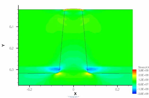
First of all, the TCAD stress simulation follows the standard STI fabrication process to realize the device structure. It includes the substrate, pad oxide, nitride deposition, STI lithography mask, STI Etching, annealing, TEOS deposition, and fake STI CMP. Main reasons for the stress origin and the lattice mismatch induced stress. Fig.8 shows the contours of stress across the whole device. We choose the stress under the surface of 2nm, which means actual carrier transport region for our device analysis. Fig.9 demonstrates the stress distribution along the channel width. Also, Fig.10 compares our simulation result with that Shih of etal. [18], compare results can be seen similar. At the same time, by using Fig.11 we can use our simulation to separate the channel stress into the average edge stress and the average flat region stress.
In 2006, Thompson etal. [15] provides the energy level calculation relation between Stress and mobility shift. At the low strain condition, the mobility enhancement is
(4-3)
were
/
is the fractional change in mobility
and
are the longitudinal and transverse stress, and the and are the longitudinal and transverse piezoresistance coefficients express by Pa-1 respectivelyThe complete summary of the piezoresistance coefficient is shown in Table 1./
4.3 TEM Picture
In the narrow device, we have taken the cross-sectional transmission electron microscopy (TEM) (not shown in the thesis) picture of devices in the width. From the TEM results, we can take it as the reference to confirm the precise stress simulation. Unfortunately, TEM results tell us the delta width (DW) does not exist for our device.
In saturation region,
(4-4)
By fixing the channel width length, we can get the correct mobility shift from our experiment in order to extract the inner stress.
2
)^
(
2
L
Cox
Vg
Vth
W
Id
eff
4.4 Channel Length Direction related IV and Noise
Experiment
4.4.1 Vth and Mobility Shift
Fig.12 show the Vth shift for different value of gate to STI spacing (A). Fig13 shows the mobility of four devices, using calculated mobility shift by piezo-resistance coefficients. The stress extracted in Table2. Experiment shows the small spacing A gives the larger stress in our device.
4.4.2 Noise Data Analysis
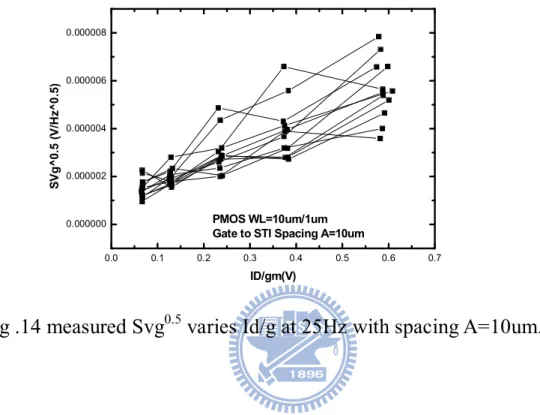
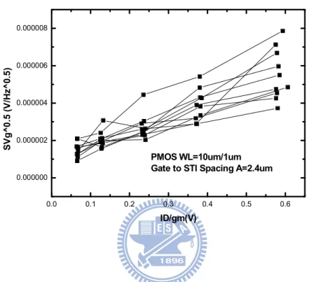
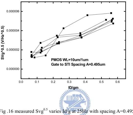
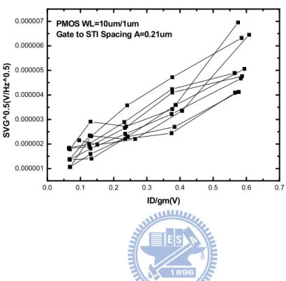
Fig.14 Fig.15 Fig.16 Fig.17 is the Svg0.5 varies Id/gm line at frequency =25Hz, Spacing A=10um, 2.4um, 0.495um, and 0.21um. Fig.18 is the fitting line for the trap density Nt (cm-3eV-1) and scattering factor α (Vs/C). Fig.19(a) and 19(b) shows the correspond Nt and α change. Although the stress change is large, and Nt has only slightly increase. The change of scattering factor is also weak.
4.5 Channel Width Direction related IV and Noise
Experiment
4.5.1 Vth and Mobility shift
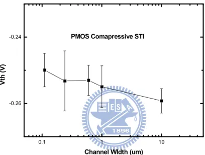
Fig.20 shows the Vth shift in narrow device, revealing that the more narrow width, the less change for Vth. It is well known that inverse narrow channel effect would apply especially in STI device process. Δ Vth~10meV was typical for edge electric field Increase, Many researches [19] suggest that the edge electrical field is more strong which makes Id current turn on more quickly.
Fig21.a is the mobility of five device (W=10,1,0.6,0.24,0.11um). If we set the x-axis as channel width, y-axis as the mobility in Vg=-0.5V, the mobility shift is very interesting. Fig.21b shows the concave up in case of narrow device, but the prediction of compressive stress effect on narrow device is presented the red line. It seems that the narrow device has different behaviors. The inverse narrow channel effect may be the suitable explanation for this phenomenon.
4.5.2 Noise Data Analysis
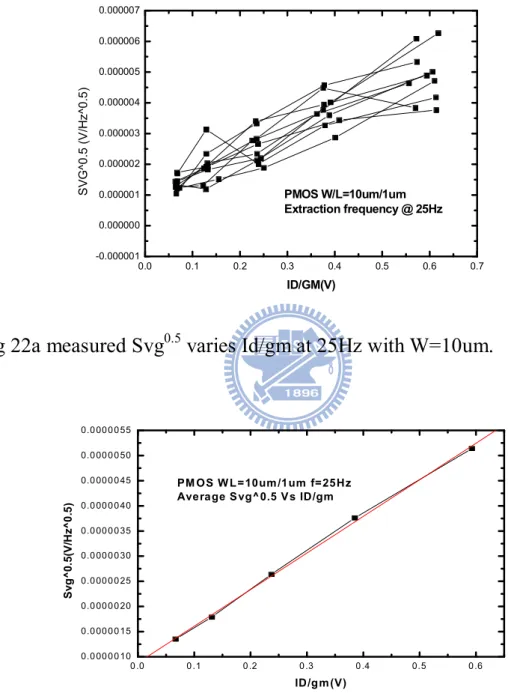
We have show in section 4.4 that more compressive stress renders device trap slitly increase. Fig22(a) , 23(a), 24(a), 25(a), 26(a) is the Svg0.5 varies Id/gm line at frequency =25Hz ,for the channel width W=10um , 1um ,0.6um,0.24u,0.11um. Fig.22(b), 23(b), 24(b), 25(b), 26(b) shows the fitting lines for the trap density Nt(cm-3eV-1) and scattering factor α (Vs/C).
Fig.27 (a) and (b) gives us more surprising results, the Nt in narrowest device (W=0.11um) is 1/8 of Nt(W-10um). In our further experiment, it is not reasonable, leading a simple assumption that more stress give more defects Nt. So, we think the narrow device corner has less trap density. It gives the reason why the average Nt is much more degraded in narrow device This structure difference overcomes the compressive stress effect in narrow channel case. Meanwhile, the scattering factor α is in the increasing trend, which can account for the mobility abnormal phenomenon in narrower device.
Chapter 5 Conclusion
In this thesis, we demonstrate the process strained silicon (PPS) induced stress distribution by the TCAD simulation. From stress induced energy level change, the mobility shift gives us another way to determine the stress in PMOS structure. Both of two methods tell us that the narrow device or a short gate to STI spacing (A) can provide enough evidence to make sure more increasing on the magnitude of the compressive stress.
By the Id/gm noise fitting method, we can extract the trap density and scattering factor. In the channel length direction, the experiment shows the STI induced stress can give more traps. However, in channel width direction, the large variation of the average trap density comes from the edge structure difference between the middle part. The I-V measurement also gives us the stress on narrow device is not the only reason for mobility change. Inverse narrow channel effect in Vth and mobility would be considered as the plausible origins for the narrow device. When we fabricate the narrow devices to increase the device number per area for cost-down, considering behavior of the narrow device in terms of the mobility, trap density, and Scattering factor should all be taken into account.
References
[1]S.E. Thompson, M. Armstrong, C. Athu, M. Alavi, M, Buehler, R. Chau, S. Cea, T.Ghani, G. Glass, T. Hoffman, C. H. Jan, C. Kenyon, J. Klaus, K. Kuhn , Z, Ma, B. Mctintyre , K. Mistry , A, Murthy, B. Obradovic, R. Nagisetty, P. Nguyen, S. Sivakumar, and R. Shaheed, IEEE
Trans. Electron Devices 51 , 1790 (2004)
[2]K. K. Hung, P. K. Ko, C. Hu, and Y. C. Chen, IEEE Trans. Electron
Devices 37, 654 (1990)
[3] M. J. Chen, T. K. Kang. Y. H. Lee, C. H. Liu , Y. J. Chang, and K. Y. Fu, J. Appl . Phys. 89, 648 (2001)
[4]Y. Taur and T. H. Ning, Fundamentals of modern VLSI Devices
Cambridge University Press, Cambridge, (1998)
[5]A. L. McWorther, Semiconductor surface physics (University of Pennsylvania Press, Philadelphia, 1957).
[6]K. K. Hung, P. K. Ko, C. Hu, and Y. C. Cheng, “A unified model for the flicker noise in metal-oxide-semiconductor field-effect transistors”,
IEEE Trans. Electron Devices 37, 654-665 (1990).
[7]S. Christensson, I. Lundstrom, and C. Svensson, “Low-frequency noise in MOS transistors-I theory”, Solid-State Electron. 11, 797-812 (1968).
[8]. E. Simoen, and C. Claeys, “On the flicker noise in submicron silicon MOSFETs”, Solid-State Electron. 43, 865-882 (1999).
[9]C. Surya and T. Y. Hsiang, “A thermal activation model for 1/f noise in Si-MOSFETs”, Solid-State Electron. 31, 959-964 (1988).
[10]G. Ghibaudo, and T. Boutchacha, “Electrical noise and RTS fluctuations in advanced CMOS devices”, Microelectron. Reliab. 42, 573-582 (2002).
[11] L. K. J. Vandamme, X. Li, and D. Rigaud, “1/f noise in MOS devices, mobility or number fluctuations? “, IEEE Trans. Electron
Devices 41, 1936-1945 (1994).
[12] J. Chang, A. A. Abidi, and C. R. Viswanathan, “Flicker noise in CMOS transistors from subthreshold to strong inversion at various temperatures”, IEEE Trans. Electron Devices 41, 1965-1971 (1994)
[13] K. K. Hung, P. K. Ko, C. Hu, and Y. C. Cheng” A physics-based MOSFET noise model for circuit simulators” IEEE trans Electron
device ,37 no.5, p1323 (1990)
[14]G. Ghibaudo, O. Roux, Ch. Nguyen-Duc, F. Balestra, and J. Brini, “Improved analysis of low-frequency noise in field-effect MOS transistors” , Phys. Stat. Sol. A 124, 571-581 (1991)
[15]Scott E. Thompson, Guangyu Sun, Youn Sung Choi, and Toshikazu Nishida, ”Uniaxial-process-induced strained-Si extending the CMOS roadmap” IEEE Trans. Electron Device VOL. 53, NO. 5 2006
[16]Ananda S. Roy and Christian C. Enz, “Critical Discussion on the Flatband Perturbation Technique for Calculating Low-Frequency Noise”
IEEE Trans. Electron Device DEVICES, VOL. 53, NO. 10 2006
[17] Chih-Yuan Chan a, Yen-Chun Huang a, Jun-Wei Chen a, Shawn S.H. Hsu a,, Ying-Zong Juang “STI-to-gate distance effects on flicker noise characteristics in 0.13 um CMOS” Solid-State Electronics 52 1182–1187(2008)
[18] J.R Shih, Robin-Wung, Y.M. Sheu, H.C Lin, J.J. Wung, and Kenneth Wu , “Pattern Density Effect of Trench Isolation-Induced Mechanical Stresson Device Reliability in sub-0.lp.m Technology”IEEE
[19]S.Matsuda, T.Sato, H.Yoshimura, Y.Takegawa, A.Sudo, I.Mizushima, Y.Tsunashima and Y.Toyoshima, “Novel Corner Rounding Process for Shallow Trench Isolation utilizing MSTS (Micro-Structure Transformation of Silicon)” P140 -IEDM 1998
Fig.1 the Energy band diagram illustration of a PMOSFET biased near the threshold point
Fig2 A schematic description of the charge distribution in the MOS
Fig.3The schematic illustration of oxide traps exchange with the channel carriers causing a fluctuation in the surface potential.
Fig4The band diagram describe the tunneling transitions, (i) directly [7] or (ii) using interface traps as stepping stones [8] from the Si to gate oxide
Fig.5 The STI structure induced stress in channel width (W) and channel length direction (L).
Device Structure
Channel Length LChannel Width (W)
Gate to STI Spacing A
Surrounding STI Stress
Surrounding STI Stress
Surrounding STI Stress Surrounding STI Stress
Gate
Bulk
Drain
Source
Fig.6The difference between id/gm and Vg-Vth fitting method. We can see that Vg-Vth is a straight line, instead id/gm is a curve .
0.2 0.3 0.4 0.5 0.6 0.7 0.0 0.1 0.2 0.3 0.4 0.5 0.6 0.7 0.8 ID /g m ( V ) Vg (V) ID/gm by Ueff Vg-Vth ID(Vd=0.025)/gm ID(Vd=0.1)/gm
ID/gm BY Noise Extraction
Fig.7 Two different fitting method (Vg-Vth, Id/gm) on the same sample. 0.0 0.1 0.2 0.3 0.4 0.5 0.6 0.000001 0.000002 0.000003 0.000004 0.000005 Sv g ^ 0 .5 ( V/ H z ^ 0 .5 ) Vg-Vth or ID/gm(V) Vg-Vth ID/gm PMOS WL=10um/1um
Fig.9 The stress distribution along the channel width. -6 -4 -2 0 2 4 6 0 200 400 600 800 1000 S tr e s s ( M P a )
Width Dirction (um)
W=10um W=1um W=0.6um W=0.24um W=0.11um
Fig.10 Comparing our simulation result with Shih[18]. 0.1 1 10 0 100 200 300 400 500 600 S tr e s s s ilu ti o n (M P a ) Channel width(um) Our Simulaiton Simulation by Shih
Fig11 The separated stress in terms of the average edge stress and average flat region stress.
0.1 1 10 0 200 400 600 800 S tr e s s ( Mp a )
Channel width (um) Flat Stress Simulation Edge Stress Simulation
Table1The Measured long p- and n-channel MOSFET piezoresistance coefficients for (001) and (110) wafers compared to bulk Si
Fig.12 The Vth shfit due to gate to STI spacing (A) induced stress. 0.1 1 10 -0.28 -0.27 -0.26 -0.25 -0.24 -0.23 V th (V )
Fig.13 The mobility shift due to gate to STI spacing (A) induced stress. -1.1 -1.0 -0.9 -0.8 -0.7 -0.6 -0.5 -0.4 -0.3 -0.2 20 30 40 50 60 70 M o b il ity (c m ^ 2 /V -s ) Vg(V) A=0.21um A=0.495um A=2.4um A=10um
Fig .14 measured Svg0.5 varies Id/g at 25Hz with spacing A=10um. 0.0 0.1 0.2 0.3 0.4 0.5 0.6 0.7 0.000000 0.000002 0.000004 0.000006 0.000008 S V g^ 0 .5 ( V /H z ^ 0 .5 ) ID/gm(V) PMOS WL=10um/1um Gate to STI Spacing A=10um
Fig .15 measured Svg0.5 varies Id/g at 25Hz with spacing A=2.4um 0.0 0.1 0.2 0.3 0.4 0.5 0.6 0.000000 0.000002 0.000004 0.000006 0.000008 PMOS WL=10um/1um Gate to STI Spacing A=2.4um
S V g ^ 0 .5 ( V /H z ^ 0 .5 ) ID/gm(V)
Fig .16 measured Svg0.5 varies Id/g at 25Hz with spacing A=0.495um 0.0 0.1 0.2 0.3 0.4 0.5 0.6 0.000000 0.000002 0.000004 0.000006 PMOS WL=10um/1um
Gate to STI Spacing A=0.495um
S V g ^ 0 .5 ( V /H z ^ 0 .5 ) ID/gm
Fig .17 measured Svg0.5 varies Id/g at 25Hz with spacing A=0.21um. 0.0 0.1 0.2 0.3 0.4 0.5 0.6 0.7 0.000001 0.000002 0.000003 0.000004 0.000005 0.000006 0.000007 PMOS WL=10um/1um
Gate to STI Spacing A=0.21um
S V G ^ 0 .5 (V /H z ^ 0 .5 ) ID/gm(V)
Fig.18 The fittings used line for extracting the trap density Nt (cm-3eV-1) and scattering factor α (Vs/C)
0.0 0.1 0.2 0.3 0.4 0.5 0.6 0.000001 0.000002 0.000003 0.000004 0.000005 0.000006 S v g ^ 0 .5 (V /H z ^ 0 .5 ) ID/gm(V) A=10um A=2.4um A=0.495um A=0.21um
Fig.19(a) The trap density Nt(cm-3eV-1). (b) the scattering factor α variation. Varies gate to STI Spacing
1 10 1E18 2E18 3E18 4E18 5E18 N t (c m -3 e V -1 )
Gate to STI Spacing A(um)
0.1 1 10 2.0x10⁴ 4.0x10⁴ 6.0x10⁴ 8.0x10⁴ 1.0x10⁵ 1.2x10⁵ 1.4x10⁵ 1.6x10⁵ 1.8x10⁵ S c a tt e ri n g F a c to r (V s /C )
Gate to STI Spacing (um)
Fig.22(a)
Fig 20 The Vth shift in narrow device, at L=1um,W=10,1,0.6,0.24, and 0.11um, 0.1 1 10 -0.26 -0.24 V th (V )
Channel WIdth (um) PMOS Comapressive STI
Fig.21a The mobility varies gate voltage of five device (W=10,1,0.6,0.24,0,11um), L=1um. 0.1 1 10 34 36 38 40 42 44 46 48 50 52 54 56 58 60 Mo b il it y ( c m ^ 2 /V -S ) Channel Width
PMOS Compressive L=1um At Vd=-0.5V
Predict Compressive
Stress Mobility Change
-1.0 -0.9 -0.8 -0.7 -0.6 -0.5 -0.4 -0.3 -0.2 35 40 45 50 55 60 65 70 75 80 85 Mo b li li ty (c m ^ 2 / V -s ) Vg(V) W=10um W=1um W=0.6um W=0.24um W=0.11um PMOS L=1um
Fig 22a measured Svg0.5 varies Id/gm at 25Hz with W=10um.
Fig 22b The fitting line at 25Hz with W=10um
0.0 0.1 0.2 0.3 0.4 0.5 0.6 0.7 -0.000001 0.000000 0.000001 0.000002 0.000003 0.000004 0.000005 0.000006 0.000007 S V G ^ 0 .5 ( V /H z ^ 0 .5 ) ID/GM(V) PMOS W/L=10um/1um Extraction frequency @ 25Hz 0 .0 0 .1 0 .2 0 .3 0 .4 0.5 0 .6 0.0 00 0 0 10 0.0 00 0 0 15 0.0 00 0 0 20 0.0 00 0 0 25 0.0 00 0 0 30 0.0 00 0 0 35 0.0 00 0 0 40 0.0 00 0 0 45 0.0 00 0 0 50 0.0 00 0 0 55 S v g ^ 0 .5 (V /H z ^ 0 .5 ) ID/g m (V) PM OS W L =10um /1um f=25Hz Average S vg^0.5 V s ID/gm
Fig 23a measured Svg0.5 varies Id/gm line at 25Hz with W=1um.
Fig 23b The fitting line at 25Hz with W=1um.
0.0 0.1 0.2 0.3 0.4 0.5 0.6 0.7 -0.000002 0.000000 0.000002 0.000004 0.000006 0.000008 0.000010 0.000012 0.000014 0.000016 0.000018 S V G ^ 0 .5 (V /H z ^ 0 .5 ) ID/gm(V) PMOS WL=1um/1um Extraction Frequency @25Hz 0.0 0.1 0.2 0.3 0.4 0.5 0.6 0.000002 0.000004 0.000006 0.000008 0.000010 0.000012 0.000014 S V G ^ 0 .5 (V /H z ^ 0 .5 ) ID/gm(V) PMOS WL=1um/1um Average SVg Vs ID/gm
Fig 24a measured Svg0.5 varies Id/gm at 25Hz with W=0.6um
Fig 24b The fitting line at 25Hz with W=0.6um
0.0 0.1 0.2 0.3 0.4 0.5 0.6 0.7 0.000002 0.000004 0.000006 0.000008 0.000010 0.000012 0.000014 0.000016 0.000018 0.000020 S V g ^ 0 .5 (V /H z ^ 0 .5 ) ID/gm(V) PMOS WL=0.6um/1um Extraction Frequency @25hz 0.0 0.1 0.2 0.3 0.4 0.5 0.6 0.000002 0.000004 0.000006 0.000008 0.000010 0.000012 0.000014 0.000016 S V G ^ 0 .5 (V /H z ^ 0 .5 ) ID/Gm(V) PMOS WL=0.6um/1um Average SVg Vs ID/Gm
Fig 25a measured Svg0.5 varies Id/gm line at 25Hz with W=0.24um
Fig 25b The fitting line at 25Hz with W=0.24um
0.0 0.1 0.2 0.3 0.4 0.5 0.6 0.7 0.000000 0.000005 0.000010 0.000015 0.000020 0.000025 0.000030 S V g ^ 0 .5 (V /H z ^ 0 .5 ) ID/Gm(V) PMOS WL=0.24um/1um Extraction Frequency @ 25Hz 0.0 0.1 0.2 0.3 0.4 0.5 0.6 0.000006 0.000008 0.000010 0.000012 0.000014 0.000016 0.000018 0.000020 0.000022 0.000024 0.000026 S V g ^ 0 .5 (V /H z ^ 0 .5 ) ID/Gm(V) PMOS WL=0.24um/1um Average SVG Vs ID/gm
Fig. 26a measured Svg0.5 varies Id/gm at 25Hz with W=0.11um
Fig. 26b The fitting line at 25Hz with W=0.11um
0.0 0.1 0.2 0.3 0.4 0.5 0.6 0.7 0.000005 0.000010 0.000015 0.000020 0.000025 0.000030 0.000035 0.000040 0.000045 S V G ^ 0 .5 (V /H z ^ 0 .5 ) ID/gm(V) PMOS WL=0.11um/1um Extraction Frequency @25Hz 0.0 0.1 0.2 0.3 0.4 0.5 0.6 0.000005 0.000010 0.000015 0.000020 0.000025 0.000030 0.000035 S V G ^ 0 .5 (V /H z ^ 0 .5 ) ID/gm(V) PMOS W/L=0.11um/1um Average SVg VS ID/Gm
Fig.27a The Trap density Nt variation in narrowing devices.
Fig.27b The scattering factor α variation in narrowing devices.
0.1 1 10 1E17 1E18 N T ( c m -3 e V -1 ) Channel Width(um) 0.1 1 10 5.0x10⁴ 1.0x10⁵ 1.5x10⁵ 2.0x10⁵ 2.5x10⁵ 3.0x10⁵ S c a tt e ri n g F a c to r (V s /C )