多極磁性元件之設計與製作在高精密定位系統之應用
113
0
0
全文
(2) 多極磁性元件之設計與製作 在高精密定位系統之應用. Design and Fabrication of Multi-Pole Magnetic Components for High Precision Position System Application. 研 究 生 : 邱國基. Student : Kuo-Chi Chiu. 指導教授 : 謝漢萍博士. Advisors : Dr. Han-Ping D. Shieh. : 黃得瑞博士. 國 立 交 通 大 學. : Dr. Der-Ray Huang. 電 機 資 訊 學 院. 光 電 工 程 研 究 所 博 士 論 文 A Dissertation Submitted in Partial Fulfillment of the Requirements for the Degree of Doctor of Philosophy in The Institute of Electro-Optical Engineering College of Electrical Engineering and Computer Science National Chiao Tung University Hsinchu, Taiwan. 中. 華. 民. 國. 九十五. 年. 三. 月.
(3) 摘. 要. 時序進入微米及次微米的時代,並已投入對奈米尺寸的技術開發,各種量測 儀器的精密度不斷地被要求提升以符合所需。由於編碼器是精密量測系統中不 可或缺的關鍵元件,因此開發一個小尺寸具有高解析度的編碼器,來增進量測 系統的功能為一重要的基本研究。一般而言,編碼器可分為兩類,一為光學式, 利用光反射或是透射的特性,造成光線明暗的效果,來作為偵測的訊號;另一 為磁性式,藉由磁性南極與北極的差異,來作為檢測的訊號。 磁性編碼器是由一個磁性感測器,以及一個多極磁性元件具有微小磁極距所 組成,解析度的高低由磁極距的大小所決定。使用傳統的方法,要製作出磁極 距小於 1mm 是非常困難的,精密的機械加工技術以及昂貴且複雜的充磁系統是 必備的條件。為了克服製作微小磁極距小於 1mm,來提升磁性編碼器的解析能 力,本論文所提出的創新方法,是利用印刷電路板的製程技術,來製作出一特 殊的線路圖形於基板上,具有均勻的磁極結構,依據安培定律,在供給線路電 流之後,便會感應產生出交錯且規則的磁場分佈,從而獲得一多極磁性元件具 有微小磁極距。 為了量測此微小磁極距的磁場分佈,我們設計製作出一個精密的磁場量測系 統,使用高解析度的霍爾探棒,其感測面積只有 165×165µm2,因此可以量測出 微小磁極距小於 1mm。不同多極磁性元件具有微小磁極距 300µm、350µm 和 400µm,已成功製作出來,同時也量測出其表面上方 200µm 與 300µm 處的磁場 分佈變化,清楚的磁性邊界顯示出此微小磁極距的大小,分別為 300µm、350µm 和 400µm。因此,磁性編碼器的解析能力可以大幅地提升 3.33 倍 (1mm/300µm)。 此外,利用有限函數疊加計算微小磁極距內之磁場公式也已經推導出來,理論 計算的數值與實驗量測的結果有很好的一致性。 另外,藉由使用雙層的線路結構,可以將其微弱的磁場強度有效地提升 1.37 倍。再者,在磁場最佳化的研究中,使用不同的線路寬度 190µm 與 235µm,其 所對應出來的最佳磁極距大小為 465µm 與 495µm,相較於其他尺寸的磁極距, 具有較大的磁場強度與變化,上述這些特性是非常有助於後續訊號的檢測與處 理。印刷電路板的製程技術已經驗證可以有效地縮減磁極距小於 1mm,不需要 精密的機械加工技術,以及昂貴複雜的充磁系統,而且大量生產很容易,不同 磁極數目與磁極距尺寸也可以輕易的完成於基板上。.
(4) Design and Fabrication of Multi-Pole Magnetic Components for High Precision Position System Application Student : Kuo-Chi Chiu. Advisors : Dr. Han-Ping D. Shieh : Dr. Der-Ray Huang. Institute of Electro-Optical Engineering National Chiao Tung University Abstract Micro-, submicro- and nano-related industries have been growing rapidly in recent years. The technologies of precise measurements thus become increasingly more demanding.. Since encoders are the key component in precise control systems,. developing a high-resolution and small-sized encoder is essential to enable the systems more competitive in performance and price. Encoders can be classified into optical and magnetic types. the light reflection or transmission as the detection signals.. The optical type uses The magnetic type. utilizes magnetic south and north poles as the sensing sources. A magnetic encoder comprises a magnetic sensor and a multi-pole magnetic component with a fine magnetic pole pitch. A smaller magnetic pole pitch yields a higher resolution in applications.. Using traditional methods, a multi-pole magnetic component. magnetized with a fine magnetic pole pitch of less than 1mm is very difficult to achieve. Moreover, it requires a precise mechanical processing and a complicated magnetization system. In order to overcome the limitation of 1mm in fabricating the magnetic pole pitch, an innovative method by using the printed circuit board (PCB) technology was employed. A special wire circuit pattern was designed and fabricated on the PCB with a periodic structure.. According to Ampere’s Law, an alternate and regular. magnetic field distribution is induced after applying a current to the wire circuit..
(5) Thus, a multi-pole magnetic component with a fine magnetic pole pitch is obtained. Additionally, a precise magnetic field measuring system was designed and set up to measure the field distribution in the fine magnetic pole pitch. A high-sensitivity Hall-effect probe with a fine sensing area of 165×165µm2 was used and therefore it is capable of determining the field distribution with a fine magnetic pole pitch of less than 1mm. Various multi-pole magnetic components with different magnetic pole pitches of 300µm, 350µm and 400µm were accomplished. The field distributions were measured at the detection spacing of 200µm and 300µm above the surface of the wire circuit. The explicit boundaries between magnetic poles are found, indicating the fine magnetic pole pitches are 300µm, 350µm and 400µm, respectively. Correspondingly, the resolution of magnetic encoders can be markedly improved by a factor of 3.33 (1mm/300µm).. Moreover, the field formulae for computing the field. distribution in the fine magnetic pole pitch have been also derived. These field solutions are expressed in terms of finite sums of elementary functions and easily implemented in any programming environments. As a comparison, the calculated values of magnetic flux density in the z direction agree with the measurement data. A dual-layered wire circuit structure was used to improve the field strength. After measurements, a gain factor of 1.37 was obtained in the field enhancement. Furthermore, various wire widths of 190µm and 235µm were used to investigate the field optimization and the corresponding optimal magnetic pole pitches are 465µm and 495µm. Such an optimal design has larger strength and steeper variation in the field distribution. Both of them are useful to the signal detection and processing. PCB manufacturing technology has been demonstrated to effectively fabricate a multi-pole magnetic component with a fine magnetic pole pitch to be less than 1mm. This innovative method provides a simple process without using the complicated technologies such as machining technique, magnetizing head and magnetization machine. Additionally, it is also a cost-effective method to enable mass production easily. Different pole numbers and pitch sizes can be also easily fabricated on the PCB through this flexible approach..
(6) Acknowledgements. I am deeply indebted to my thesis advisors, Professor Han-Ping D. Shieh and Professor Der-Ray Huang, for conducting me to pursue my advanced degree in the area of applied magnetism at National Chiao Tung University. This thesis provides a very unique opportunity for scientific research as well as engineering development in the technology of high-precision control system. Working for Professor Shieh and Professor Huang has been rewarding in many aspects. I am very grateful to the thesis committee members for their constructive and invaluable suggestions on this research. The financial and various technical supports from ITRI are also greatly appreciated.. I especially acknowledge Mr. Chin-Sen. Chen for his continuous efforts to make this research work possible. I also wish to thank my colleagues in ITRI for their constant encouragement, advice and help on some research subjects. Finally, I would like to express my sincere appreciation to my parents and family for their patience and encouragement during the years of my study. The sharing of joy and frustration with my wife on my thesis work is an essential element in the completion of this thesis..
(7) To my Parents and my Wife.
(8) Contents. Chapter 1 Introduction ..................................................................................... 1 1.1 Overview of encoders ....................................................................... 1 1.2 Optical encoder ................................................................................ 2 1.3 Magnetic encoder ............................................................................. 3 1.4 A review of magnetic encoders related technologies ............................ 4 1.4.1 Linear types of multi-pole magnetic components ....................... 5 1.4.2 Rotary types of multi-pole magnetic components ...................... 8 1.4.3 Summary .............................................................................. 13 1.5 Motivation and objective of this dissertation ...................................... 14 1.6 Organization of this dissertation ........................................................ 15. Chapter 2 Design and fabrication ................................................................. 17 2.1 Introduction .................................................................................... 17 2.2 Design ............................................................................................ 21 2.3 Fabrication ..................................................................................... 23 2.3.1 Drawing ................................................................................ 23 2.3.2 Wire circuit manufacturing process ......................................... 25 2.4 Summary ........................................................................................ 28. I.
(9) Chapter 3 Theoretical analysis ...................................................................... 29 3.1 Long and straight wire ..................................................................... 29 3.2 Straight wire with a finite length L .................................................... 30 3.2.1 Point P located outside the straight wire .................................. 30 3.2.2 Point P loacted along the bisection line of the straight wire ....... 32 3.2.3 Point P located at the upper position of the straight wire ........... 33 3.2.4 Point P located at the lower position of the straight wire ........... 34 3.3 Two-dimensional analysis ................................................................ 34 3.4 Three-dimensional analysis .............................................................. 36 3.5 Field analysis .................................................................................. 37 3.5.1 At Area 1 .............................................................................. 39 3.5.2 At Area 2 .............................................................................. 39 3.5.3 At the top side of Area 3 ........................................................ 40 3.5.4 At the bottom side of Area 3 ................................................... 41 3.5.5 At the top side of Area 4 ........................................................ 42 3.5.6 At the bottom side of Area 4 ................................................... 43 3.5.7 At Area 5 .............................................................................. 44 3.5.8 At the left side of Area 6 ........................................................ 45 3.5.9 At the right side of Area 6 ...................................................... 45 3.6 Summary ........................................................................................ 48. II.
(10) Chapter 4 Field measurements ...................................................................... 50 4.1 Dimensional measurements .............................................................. 50 4.2 Magnetic field measuring system ...................................................... 53 4.3 Measurement results ........................................................................ 55 4.4 Summary ........................................................................................ 60. Chapter 5 Field enhancement and optimization ....................................... 61 5.1 Field enhancement ........................................................................... 61 5.1.1 Design and experiments ......................................................... 61 5.1.2 Results and discussions .......................................................... 63 5.1.3 Summary .............................................................................. 66 5.2 Field optimization ........................................................................... 67 5.2.1 Design and experiments ......................................................... 67 5.2.2 Results and discussions .......................................................... 69 5.2.3 Summary .............................................................................. 71. Chapter 6 Field variation analysis ................................................................ 72 6.1 Variation among different multi-pole magnetic components ................ 72 6.2 Variation along different measuring routes ......................................... 73 6.3 Summary ........................................................................................ 77. III.
(11) Chapter 7 Conclusions ..................................................................................... 78. References ........................................................................................ 82. Appendix .......................................................................................... 86. IV.
(12) List of Figures Fig. 1-1.. Configurations of (a) a linear, (b) 2D and (c) rotary optical. 2. encoders. Fig. 1-2.. (a) An optical encoder used in the inkjet printer. (b) Enlarged. 3. photo of the optical grating element. Fig. 1-3.. Configurations of (a) a linear, (b) 2D and (c) rotary magnetic. 4. encoders. Fig. 1-4.. (a) A magnetic encoder employed in the lens module. (b) Enlarged. 4. photo of the multi-pole magnetic component. Fig. 1-5.. Linear types of a magnetizing head and (b) a multi-pole magnetic. 6. component on a magntiec sheet. Fig. 1-6.. Magnetic moments exist inside the magnetic material (a) before. 6. magnetization and (b) after magnetization. Fig. 1-7.. A LPM mover used in the magnetic encoder with a tooth structure. 7. as a multi-pole magnetic component. Fig. 1-8.. Output voltage varied with the bias gap δb and tooth pitch τ.. 8. Fig. 1-9.. Rotary types of multi-pole magnetic components (a) in the axial. 8. and (b) in the radial directions for various applications. Fig. 1-10. (a) Schematic view of the magnetizing fixture in the axial. 9. direction. (b) Configuration of the winding pattern in the magnetizing fixture. (c) Photos of the fixture base and magnetizing fixture. Fig. 1-11. (a) Configuration and (b) photo of a unique magnetizing head.. 10. Fig. 1-12. (a) Schematic view and (b) photo of a multi-pole magnetic drum. 11. (magnetic component) with a fine magnetizing pitch λ mounted on the base. Fig. 1-13. (a) Photo and (b) schematic view of a precise multi-pole. 12. magnetization system including a magnetizing head and a magnetization machine.. Fig. 2-1.. Magnetic flux density distribution in a long and straight wire.. 18. Fig. 2-2.. (a) Linear wire circuit pattern with a periodic structure. (b) The. 19. magnetic flux density distribution induced from the linear wire circuit pattern.. V.
(13) Fig. 2-3.. (a) Annular wire circuit pattern with a multi-pole configuration in. 19. the radial direction. (b) The magnetic flux density distribution induced from the annular wire circuit pattern. Fig. 2-4.. Special wire circuit pattern designed for fabricating a multi-pole. 21. magnetic component with a fine magnetic pole pitch. Fig. 2-5.. (a) Schematic view of the cross section on the special wire circuit. 22. pattern along the bisection line. (b) The magnetic flux density distribution generated from the special wire circuit pattern. Fig. 2-6.. Schematic view of the cross section on a dual-layered wire circuit. 22. structure along the bisection line. Fig. 2-7.. Geometrical structures of (a) single-layered and (b) dual-layered. 23. wire circuits. Fig. 2-8.. Various drawings of nine-pole magnetic components with different. 24. fine magnetic pole pitches of (a) 250µm by using a wire width of 100µm and a gap of 150µm, (b) 300µm by using a wire width of 100µm and a gap of 200µm, (c) 250µm by using a wire width of 125µm and a gap of 125µm, and (d) 300µm by using a wire width of 125µm and a gap of 175µm. Fig. 2-9. (a) Nine-pole and (b) nineteen-pole wire circuit masks.. 25. Fig. 2-10. Flow charts of wire circuit manufacturing process. (a) The surface. 26. of the copper film is cleaned up to be free from dusts. (b) A photoresist layer is applied to the surface of the copper film. (c) A pre-prepared mask is placed on the top of the photoresist layer. (d) The UV light is employed to proceed the light exposure process. (e) The non-exposed area is removed through a developing process. (f) The copper film at the exposed area is removed by chemical reaction using an etching solvent. (g) The residual photoresist on the surface of the wire circuit is stripped. (h) The wire circuit is accomplished on the substrate. Fig. 2-11. A nine-pole magnetic component fabricated on the PCB with a. 27. fine magnetic pole pitch of 350µm by using a wire width of 175µm and a gap of 175µm. Fig. 2-12. A 29-pole magnetic component fabricated on the PCB with a fine magnetic pole pitch of 500µm by using a wire width of 225µm and a gap of 275µm.. VI. 28.
(14) Fig. 3-1.. Long and straight wire carrying a steady current I, the element dl r contributes a dB at the point P.. 30. Fig. 3-2.. A straight wire with a finite length L carrying a steady current I, r the element dz’ contributes a dB at the point P located outside the. 31. straight wire. Fig. 3-3.. A straight wire with a finite length L carrying a steady current I, r the element dz’ contributes a dB at the point P located along the. 32. bisection line of the straight wire. Fig. 3-4.. A straight wire with a finite length L carrying a steady current I, r the element dz’ contributes a dB at the point P located at the. 33. upper position of the straight wire. Fig. 3-5.. A straight wire with a finite length L carrying a steady current I, r the element dz’ contributes a dB at the point P located at the. 34. lower position of the straight wire. Fig. 3-6.. Mesh of a straight wire with a finite length L carrying a steady. 35. current I and the wire width T 1 ≈ r . The distance rn1 decreases slightly with a small t1. Fig. 3-7.. (a) Mesh and (b) corresponding postions of all elements of a. 36. straight wire with a wire width T 1 ≈ r and a wire thickness T 2 ≈ r carrying a steady current I. The distances of rn1 and zn 2 decrease slightly with a small t1 and t2, respectively. Fig. 3-8.. (a) Geometrical structure, current loop and induced field direction. 38. of the wire circuit. (b) Corresponding positions of each segment and six areas indicated with different colors for study separately. Fig. 3-9.. Top view of the central pole on the PCB sample and the. 47. corresponding cross section of the wire circuit. Fig. 3-10. Calculated field distributions of the central pole along the bisection. 48. line for the magnetic pole pitch of 300µm at the detection spacing of 200µm and 300µm. Fig. 3-11. Calculated field distributions of the central pole along the bisection line for the magnetic pole pitch of 400µm at the detection spacing of 200µm and 300µm.. VII. 48.
(15) Fig. 4-1.. Precise dimension measuring system.. 51. Fig. 4-2.. (a) Image of wire circuit captured and displayed on the monitor. 52. through CCD module. (b) Enlarged image of copper wires on the PCB sample. Fig. 4-3.. (a) Sample of part copper wires fixed by using the acrylic resin. (b). 53. Enlarged images of the thickness of part copper wires fabricated on the PCB sample. Fig. 4-4.. Precise magnetic field measuring system.. 54. Fig. 4-5.. Top view of the three central poles on nine-pole magnetic. 55. components and the corresponding cross section. Fig. 4-6.. Field distributions at the detection spacing of 200µm and 300µm. 56. for the magnetic pole pitch of 300µm (T1/G=5/7). Fig. 4-7.. Field distributions at the detection spacing of 200µm and 300µm. 56. for the magnetic pole pitch of 350µm (T1/G=6/8). Fig. 4-8.. Field distributions at the detection spacing of 200µm and 300µm. 57. for the magnetic pole pitch of 400µm (T1/G=7/9). Fig. 4-9.. Field distributions with various ratios of T1/G at the detection. 58. spacing of 200µm. Fig. 4-10. Field distributions with various ratios of T1/G at the detection. 58. spacing of 300µm. Fig. 4-11. Field distributions of the central pole along the bisection line with. 59. various ratios of T1/G at the detection spacing of 200µm. Fig. 4-12. Field distributions of the central pole along the bisection line with. 60. various ratios of T1/G at the detection spacing of 300µm.. Fig. 5-1.. Cross section, induced magnetic field and equivalent circuit of DL. 62. wire circuit structure. Fig. 5-2.. Field distributions for the magnetic pole pitch of 500µm at the. 64. detection spacing of 200µm and 300µm with SL wire circuit structure. Fig. 5-3.. Field distributions for the magnetic pole pitch of 500µm at the. 64. detection spacing of 200µm and 300µm with DL wire circuit structure. Fig. 5-4.. Field distributions for the magnetic pole pitch of 500µm at SL and DL wire circuit structures.. VIII. 65.
(16) Fig. 5-5.. Calculated values and measurement data of the central pole for the. 66. magnetic pole pitch of 500µm on SL wire circuit structure. Fig. 5-6.. Calculated values and measurement data of the central pole for the. 66. magnetic pole pitch of 500µm on DL wire circuit structure. Fig. 5-7.. (a) Geometical structure of a straight wire with a finite length. (b). 68. The field distribution calculated along the bisection line at at the detection spacing of 200µm. Fig. 5-8.. Pole structure and optimal condition in the field distribution.. 68. Fig. 5-9.. Field distributions of the central pole at different magnetic pole. 70. pitches of 365µm, 465µm and 565µm by using the wire width T1 of 190µm. Fig. 5-10. Field distributions of the central pole at different magnetic pole. 70. pitches of 395µm, 495µm and 595µm by using the wire width T1 of 235µm.. Fig. 6-1.. Field distributions along the bisection line among different 9-pole,. 73. 19-pole, and 29-pole magnetic components with a fine magnetic pole pitch of 500µm. Fig. 6-2.. Different measuring routes with various wire segments b.. 73. Fig. 6-3.. Field distributions along different measuring routes in the 9-pole. 74. magnetic component with a fine magnetic pole pitch of 400µm. Fig. 6-4.. Field distributions along different measuring routes in the 19-pole. 75. magnetic component with a fine magnetic pole pitch of 400µm. Fig. 6-5.. Field distributions of the central pole along different measuring. 76. routes in the z direction for the 9-pole magnetic component. Fig. 6-6.. Field distributions of the central pole along different measuring routes in the z direction for the 19-pole magnetic component.. IX. 76.
(17) List of Tables Table 2-1 Comparison among different methods. 20. Table 4-1 Various wire widths T1, gaps G, pitch sizes, and ratios of T1/G. 55. Table 5-1 Parameters on DL wire circuit structure. 63. Table 5-2 Parameters of wire width T1, distance rmax, gap G and optimal. 69. magnetic pole pitch T1+G Table 6-1 ious values of magnetic flux density at various wire segments b for 9-pole and 19-pole magnetic components. X. 75.
(18) Chapter 1 Introduction. Chapter 1. Introduction. The principles and configurations of different optical and magnetic encoders are presented. A review of magnetic encoders related technologies are also reported and some critical issues with respect to the improvement of performance are considered as well.. Finally, the motivation, objective and organization of this dissertation are. discussed.. 1.1. Overview of encoders. Micro-, submicro- and nano-related industries have been growing rapidly in recent years. The technologies of precise measurements thus become increasingly more demanding.. Since encoders are the key component in precise control systems,. developing a high-resolution and small-sized encoder is essential to enable the systems more competitive in performance and price. Encoders can be classified into optical and magnetic types. Both of them are widely used to detect the position, angle or speed in precise control systems. They are playing an important role in Information Application (IA) products, in automatic manufacturing for various industries, etc. Consequently, encoders can be frequently found in different places such as lathes for the precise machining, printers for the precise printing and optical disc drives for the precise reading, etc. The performance of magnetic encoders is now comparable to that of optical types. They are rigid with a simple structure to offer a reliable operation in adverse. 1.
(19) Chapter 1 Introduction. environments with large vibration, high temperature, dense moisture or dust.. Since. encoders are only an auxiliary element in a system, they do not much attract the mainstream academic and industrial attentions. Only a few scholars and researchers had been interested in and devoted to the research of this important key component [1-19]. Both of optical and magnetic encoders will be introduced in the following sections.. H. High reflection. Low reflection. L. Optical sensor Linear optical encoder H. L. H. L. H. L. H. L. H. L. Optical grating element. H. L. H. L. H. L. Optical grating pitch (a) Rotary optical encoder. 2D optical encoder. Optical sensor. L H. L. H. L. L. H. L. H. H H. High reflection. L. L. H H. H. L. H. L. L. H. L. H. L. Optical sensor. H. L. Low reflection H. (b). High reflection. L. Low reflection. (c). Fig. 1-1. Configurations of (a) a linear, (b) 2D and (c) rotary optical encoders.. 1.2. Optical encoder. An optical encoder comprises an optical sensor and an optical grating element with a fine grating pitch.. A smaller pitch size yields a higher resolution in. applications. Figure 1-1 shows the configurations of various linear, 2D and rotary optical encoders, respectively. The high (H) and low (L) reflection signals can be detected by using the optical sensor when the light reflects from or transmits through. 2.
(20) Chapter 1 Introduction. the optical grating element. Consequently, the precise position, angle or speed can be obtained by counting the number of high and low reflection signals. An example of an optical encoder used in the inkjet printer for controlling the precise position in printing is illustrated in Fig. 1-2. The similar high and low reflection signals are detected when the light passes through the optical grating element. After counting the number of high and low reflection signals, the precise position can be found. Accordingly, the documents can be printed out accurately.. Optical grating element. Enlarging Inkjet printer. (a). (b). Fig. 1-2. (a) An optical encoder used in the inkjet printer. (b) Enlarged photo of the optical grating element.. 1.3. Magnetic encoder. A magnetic encoder consists of a magnetic sensor and a multi-pole magnetic component with a fine magnetic pole pitch. Figure 1-3 indicates the configurations of various linear, 2D and rotary magnetic encoders, respectively. The resolution of magnetic encoders can be markedly improved by narrowing the magnetic pole pitch. Different field distributions of magnetic south (S) and north (N) poles are distinguished from the magnetic sensor. Correspondingly, the precise position, angle or speed can be acquired after counting the number of magnetic poles. An example of a magnetic encoder employed in the lens module for controlling. 3.
(21) Chapter 1 Introduction. the precise focusing when taking photographs is shown in Fig. 1-4. The precise position in focusing can be decided after accumulating the number of magnetic poles.. S. Magnetic sensor. South pole. N. North pole. Linear magnetic encoder S. N. S. N. S. N. S. N. S. N. S. N. Mult-pole magnetic component. S. N. S. N. Magnetic pole pitch (a). Magnetic sensor. Rotary magnetic encoder 2D Magnetic encoder. N. S. N. S. S. N. S. N. S. N. S. S. N. S. N. S N. N S. N. N S. N. South pole. S S. North pole. S. (b). N. Magnetic sensor. South pole. N. North pole. (c). Fig. 1-3. Configurations of (a) a linear, (b) 2D and (c) rotary magnetic encoders.. Lens module Enlarging Multi-pole magnetic component. (a). (b). Fig. 1-4. (a) A magnetic encoder employed in the lens module. (b) Enlarged photo of the multi-pole magnetic component.. 1.4. A review of magnetic encoders related technologies. Several methods have been used to fabricate a multi-pole magnetic component with a fine magnetic pole pitch for use in magnetic encoders. However, a costly and. 4.
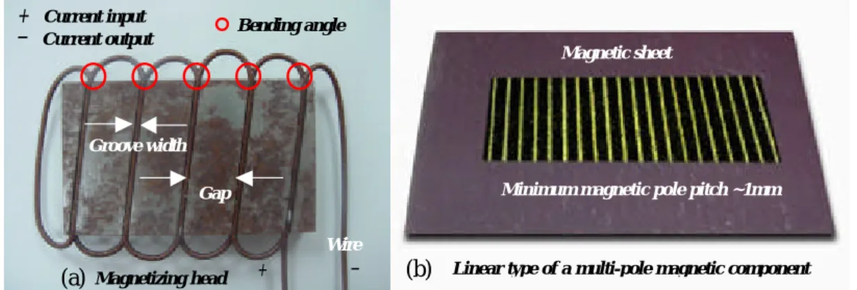
(22) Chapter 1 Introduction. complicated magnetization system including a precise magnetizing head (or fixture) and a magnetization machine is required [1-14]. During the magnetization process, an unmagnetized magnetic component is placed on the top of a magnetizing head. The magnetizing coils are wound and fixed on the magnetizing head with a multi-pole configuration. The terminals of magnetizing coils are connected to a magnetization machine, which can provide a large magnetizing current. A large magnetic field is induced instantaneously to magnetize the magnetic component into a multi-pole structure after applying a large current to the magnetizing coils. Thus, a multi-pole magnetic component can be obtained.. Different methods for fabricating various. types of multi-pole magnetic components are discussed as follows.. 1.4.1 Linear types of multi-pole magnetic components. The linear types of a magnetizing head and a multi-pole magnetic component on a magnetic sheet [20] are illustrated in Fig. 1-5. The grooves in the magnetizing head are designed for winding the magnetizing coils to form an alternate magnetic field distribution. The spacing between any two adjacent grooves is defined as the gap. The sum of groove width and gap is defined as the magnetic pole pitch, which is limited by machining techniques.. The minimum magnetic pole pitch can be. achieved only around 1mm through this approach. Additionally, the waveform of the magnetizing current should be modified to fit the material characteristic of the magnetic component to attain the optimal condition for magnetization. Before magnetization, the magnetic moments inside the magnetic material are in a random state. The net magnetic moment is zero and therefore no magnetic field exists in the magnetic component. However, the magnetic moments will move to the same direction after magnetization. Consequently, the net magnetic moment is not 5.
(23) Chapter 1 Introduction. zero and the magnetic field is thus generated in the magnetic component, as shown in Fig. 1-6.. + Current input - Current output. Bending angle Magnetic sheet. Groove width Minimum magnetic pole pitch ~1mm. Gap Wire. (a). Magnetizing head. +. -. (b). Linear type of a multi-pole magnetic component. Fig. 1-5. Linear types of a magnetizing head and (b) a multi-pole magnetic component on a magntiec sheet.. N : North pole. S : South pole. S N N. (a) Before magnetization. S. (b) After magnetization. Fig. 1-6. Magnetic moments exist inside the magnetic material (a) before magnetization and (b) after magnetization.. During the magnetization process, the magnetic sheet is placed on the top of the magnetizing head.. According to Ampere’s law, an alternate magnetic field. distribution is induced instantaneously after applying a current to the current input on the head. Accordingly, a linear type of multi-pole magnetic component is obtained [21].. The magnetizing head is made of a permalloy, which has a very high. permeability that can concentrate the magnetic flux to enhance the magnetic field for magnetization.. However, the insulating layer of magnetizing coils is easy to damage. at the large bending angle in grooves and this often leads to a short circuit. Moreover, the large magnetization energy needs to disperse in a few seconds and 6.
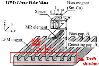
(24) Chapter 1 Introduction. therefore the magnetizing coils are broken frequently during the magnetization process.. This approach is thus very dangerous.. A method proposed by Y. Kikuchi et al. who used a linear pulse motor (LPM) mover in a magnetic encoder [22]. The LPM mover is made of carbon steel with a tooth structure as a multi-pole magnetic component.. A bias magnet is hired to. generate different magnetic resistance and a MR element is employed to detect the resistance in the tooth structure, as shown in Fig. 1-7. After counting the number of output pulses from MR element, the exact displacement is obtained.. LPM : Linear Pulse Motor LPM. Tooth pitch. Tooth structure. Fig. 1-7. A LPM mover used in the magnetic encoder with a tooth structure as a multi-pole magnetic component.. Although the tooth pitch in the LPM mover (multi-pole magnetic component) can be narrowed to around 0.8mm without using the costly and complicated magnetization system, the uniformity of LPM mover structure is not easy to control and fabricate by using conventional machining tools. Moreover, the bias gap δb and detecting gap δ d should be also carefully adjusted to obtain the maximum variation in the magnetic resistance for measurements. Additionally, a well design and alignment among the bias magnet, MR element and LPM mover are required as well. Furthermore, the output voltage from MR element is varied with the bias gap 7.
(25) Chapter 1 Introduction. δb and tooth pitch τ significantly, as illustrated in Fig. 1-8. All above-mentioned problems are difficult to handle in applications through this approach.. δ b : Bias gap. Fig. 1-8. Output voltage varied with the bias gap δb and tooth pitch τ.. 1.4.2 Rotary types of multi-pole magnetic components. Except linear types, the rotary types of multi-pole magnetic components are also widely used in precise control systems, as shown in Fig. 1-9 [20]. The components are magnetized in the axial and radial directions for various applications. Figure 110 demonstrates a rotary type of magnetizing fixture (or head) is employed to magnetize the magnetic component into an eight-pole structure in the axial direction.. (a) Axial direction. (b) Radial direction. Fig. 1-9. Rotary types of multi-pole magnetic components (a) in the axial and (b) in the radial directions for various applications.. 8.
(26) Chapter 1 Introduction. (b). Fixture base Current I. + Current input. Bending angle of grooves. Magnetic component Different directions of magnetic fields. Groove Current input. - Current output. Current output. Magnetizing fixture. Piece Fixture base. Base. (a). (c). Fig. 1-10. (a) Schematic view of the magnetizing fixture in the axial direction. (b) Configuration of the winding pattern in the magnetizing fixture. (c) Photos of the fixture base and magnetizing fixture.. Both of fixture bases (12 and 12’) are also made of a permalloy, which has a very high permeability that can concentrate the magnetic flux to enhance the magnetic field for magnetization [23-24]. The surfaces of fixtures are divided into eight equal pieces (16~30 and 16’~30’) through the line-cutting process. The magnetizing coils (15’ and 34) are wound into the grooves. An alternate multi-pole magnetic field distribution is formed from using an appropriate layout of magnetizing coils, as illustrated in Fig. 1-10 (b). Both terminals of current input (36) and output (38) are connected to a magnetization machine.. A large magnetic field is induced. instantaneously after the magnetization machine releases a large magnetizing current. The magnetic component (40) is then magnetized into an eight-pole structure. Unfortunately, the same problem also occurs in this rotary type of magnetizing fixture, as discussed in the linear type.. The insulating layer of magnetizing coils can. not withstand the stress and finally results in break. Consequently, a short circuit 9.
(27) Chapter 1 Introduction. happens between the bases of magnetizing fixtures.. Since both bases are made of a. permalloy, the magnetizing coils and fixtures are often exploded during the magnetization process. The risk of explosion can not be avoided because the large magnetic field is required for reversing the magnetic moments inside the magnetic material. The sum of groove width and piece size is defined as the magnetic pole pitch, which is also limited by machining techniques. Accordingly, it is not easy to have a fine magnetic pole pitch of less than 1mm through this approach.. Air gap Unique magnetizing head. Leakage gap. Unique magnetizing head. Magnetic component. Base Spindle motor. (a). (b). Fig. 1-11. (a) Configuration and (b) photo of a unique magnetizing head.. In order to overcome the limitation of 1mm in fabricating the fine magnetic pole pitch, a single-pulse magnetization method, which resembles the magnetic recording technology, was introduced [25]. Figure 1-11 (a) shows the magnetizing coils are wound and fixed on a unique magnetizing head. A leakage gap exists in the head to leak out the magnetic flux to record magnetic pole pairs (i.e. N and S pole) onto the surface of the plastic ferrite permanent magnet wheel (magnetic component). The magnetic pole pitch of less than 1mm can be achieved by using this method. Before magnetization, the magnetic component is mounted on a base that is usually supported and rotated through a high-precision spindle motor, as shown in Fig. 1-11. 10.
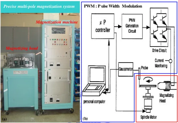
(28) Chapter 1 Introduction. (b). The precise position control of the spindle motor is highly required; otherwise, an asymmetric magnetic field distribution will appear on the multi-pole magnetic component after magnetization. The asymmetric magnetic field distribution is not useful to the subsequent processing of signals. After magnetization, a multi-pole magnetic drum (magnetic component) with a fine magnetizing pitch λ is obtained, as shown in Fig. 1-12. A precise MR element is employed to determine the field distribution generated from the multi-pole magnetic drum.. Multi-pole magnetic drum. (a). Fig. 1-12.. (b). Base. (a) Schematic view and (b) photo of a multi-pole magnetic drum. (magnetic component) with a fine magnetizing pitch λ mounted on the base.. A precise multi-pole magnetization system comprises a magnetizing head and a magnetization machine, as shown in Fig. 1-13 (a). The red mark in Fig. 1-13 (b) represents the unit of the magnetizing head, as discussed in Figs. 1-11(a) and 1-12(a). The blue area indicates the unit of the magnetization machine, as illustrated in Fig. 113 (b). The field distributions of multi-pole magnetic components are detected by using a Gauss meter with a precise Hall-effect probe. The precise position of the spindle motor is controlled through the µP controller. The magnetic pole pairs are recorded intermittently onto the surface of the magnetic component through the pulse. 11.
(29) Chapter 1 Introduction. width modulation (PWM) generation circuit and drive circuit. All tasks are carefully handled by the personal computer.. Precise multi-pole magnetization system. PWM : P ulse Width Modulation. Magnetization machine. Magnetizing head. (b). (a). Fig. 1-13. (a) Photo and (b) schematic view of a precise multi-pole magnetization system including a magnetizing head and a magnetization machine.. During the magnetization process, the magnetic component will often collide with the head if its radial run-out is too large and thus results in damages on both of them. Consequently, the dimension of the magnetic component must be fabricated uniformly with a small radial run-out. Moreover, the leakage gap in the head and the air gap between the head and magnetic component must be properly adjusted to obtain the desired magnetic pole pitch.. As the magnetic pole pitch gets smaller, both of. leakage and air gaps need to be narrowed as well.. These are key factors to affect the. size of the magnetic pole pitch in magnetization. Furthermore, the waveform of the magnetizing current from the magnetization system is required to modify to fit the magnetic material property of the magnetic 12.
(30) Chapter 1 Introduction. component. In addition to the tiny radial run-out and material homogeneity, the magnetic component must be mounted on a spindle motor under a precise position control.. All requirements for magnetization can be achieved only through the. precise multi-pole magnetization system. Despite the fact that the single-pulse magnetization method can narrow the magnetic pole pitch to be less than 1mm, the fabrication process is very difficult and complicated. Additionally, the precise machining technique, magnetizing head and magnetization machine are also necessary.. Consequently, the single-pulse. magnetization method is costly in fabricating a multi-pole magnetic component with a fine magnetic pole pitch.. 1.4.3 Summary. Several methods have been discussed to fabricate a multi-pole magnetic component with a fine magnetic pole pitch. For practical applications, some critical issues are required for narrowing the magnetic pole pitch as mentioned as the following :. n. Precise machining To fabricate the magnetic component with a small radial run-out for. magnetization.. n. Magnetizing head (fixture) To magnetize the magnetic component into a multi-pole structure with a fine. magnetic pole pitch.. 13.
(31) Chapter 1 Introduction. n. Magnetization machine To supply and modify the magnetizing current to fit the material characteristic of. the magnetic component.. 1.5. Motivation and objective of this dissertation. A wide magnetic pole pitch is insufficient for high-resolution control applications. Traditionally, a magnetizing head, which is used to magnetize the magnetic component into a multi-pole structure, is fabricated through the line-cutting process. Since the process is highly depended upon the precision of machining tools, it is difficult to have a fine magnetic pole pitch of less than 1mm. The single-pulse magnetization method, which resembles the magnetic recording technology, is also mentioned to fabricate a multi-pole magnetic component. Finally, the limitation of 1mm in the magnetic pole pitch is overcome by using this costly and complicated method. In view of foregoing problems in narrowing the magnetic pole pitch, the precise magnetizing head and magnetization machine are required. Additionally, the precise machining techniques are essential to produce the magnetic component with a small radial-runout for magnetization.. In order to overcome the different technical. barriers, creating an innovative method with a simple process to fabricate a multipole magnetic component with a fine magnetic pole pitch of less than 1mm is the motivation of this dissertation. PCB manufacturing technology has been applied to many products and gained a great success at various industrial applications. More and more electric devices can be placed on a substrate and the corresponding wire circuit density is thus higher and higher than before. According to electromagnetism, applying a current to a long and 14.
(32) Chapter 1 Introduction. straight wire will induce an annular magnetic field around the wire. The magnetic flux density is proportional to the current input, but inversely proportional to the distance [26]. Consequently, an alternate and regular magnetic field distribution can be obtained from designing a special wire circuit pattern with an appropriate layout. Thus, a multi-pole magnetic component can be accomplished by forming the special wire circuit pattern on the PCB. The objective of this dissertation is to fabricate a multi-pole magnetic component with a fine magnetic pole pitch by using the PCB manufacturing technology. At present, the minimum wire width and the gap between any two adjacent wires on the circuit can be achieved are about 3mils (~75µm, 1mil = 25.4µm) through the PCB manufacturing technology. Correspondingly, it is highly possible to have a fine magnetic pole pitch of less than 1mm. The first goal of this thesis is to design and fabricate a special wire circuit pattern having a multi-pole structure with a fine magnetic pole pitch of less than 1mm on the PCB. Since the induced magnetic fields among the wire circuits are very small, the field distributions in the fine magnetic pole pitch are not easy to detect. Accordingly, the second goal of this thesis is to develop a high-precision magnetic field measuring system to determine the field distributions in the fine magnetic pole pitch.. It. combines a precise Gauss meter, a Hall-effect probe, a probe holder, a PCB sample holder, an X-Y micro-stage, and an X-Y-Z micro-stage. All of them are mounted on an optical table to prevent vibrations.. 1.6. Organization of this dissertation. This dissertation is organized as the following : An introduction is reported in Chapter 1. Design and fabrication of a multi-pole magnetic component with a fine 15.
(33) Chapter 1 Introduction. magnetic pole pitch by using the PCB manufacturing technology are discussed in Chapter 2. Both of linear and rotary types of wire circuit patterns are presented to form different multi-pole magnetic components on the PCB. In Chapter 3, the field formulae for computing the magnetic flux density distribution in the fine magnetic pole pitch are derived through the theoretical analysis.. In Chapter 4, a precise. magnetic field measuring system is designed and set up to determine the field distributions induced from the wire circuits. In Chapter 5, the field enhancement using a dual-layered wire circuit structure is studied to improve the field strength for measurements. investigated.. The field optimization in the fine magnetic pole pitch is also Moreover, the field variations along different measuring routes are. analyzed in Chapter 6. Finally, the conclusions with a summary of main results and areas for future works in this dissertation are presented in Chapter 7. All programs for computing the field distribution in the fine magnetic pole pitch are given in Appendix.. 16.
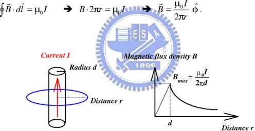
(34) Chapter 2 Design and fabrication. Chapter 2. Design and fabrication. An innovative method by using the printed circuit board (PCB) manufacturing technology is employed to fabricate a multi-pole magnetic component with a fine magnetic pole pitch of less than 1mm. Neither the precise machining technique or the magnetizing head and magnetization machine is required.. This innovative. method is not only a simple but also a cost-effective method to enable mass production easily. Additionally, different pole numbers and pitch sizes can be also easily achieved by modifying an appropriate wire circuit pattern on the PCB.. 2.1 Introduction. Several technologies have been described to fabricate a multi-pole magnetic component with a fine magnetic pole pitch in Chapter 1. However, the costly and complicated machining technique, magnetizing head and magnetization machine are required. Unfortunately, these techniques are difficult to be held simultaneously. PCB manufacturing technology has been widely used and gained a great success in many products for various industrial applications. More and more electric devices can be placed on a substrate. Consequently, the wire circuit density is thus higher and higher than before. Since the wire circuit fabricated on the PCB is made of copper, it can be treated as composed of many straight wires that are located at different positions on the substrate. According to electromagnetism [27], an annular magnetic field is induced around. 17.
(35) Chapter 2 Design and fabrication. a long and straight wire after applying a steady current, as shown in Fig. 2-1. The r magnetic flux density B inside the wire is given by. r r B ∫ ⋅ dl = µ0 I. πr 2 è B ⋅ 2πr = µ0 I 2 πd. r è B = µ0 I. r φˆ, 2πd 2. where r is the distance, d is the radius of the wire, I is the current input,. (2-1). φˆ. is the unit. vector in cylindrical coordinates and µ0 is the permeability of free space. Outside r the wire, the magnetic flux density B is proportional to the current input I but inversely proportional to the distance r, and it is. r r B ∫ ⋅ dl = µ0 I. è B ⋅ 2πr = µ0 I. Current I. r µI è B = 0 φˆ. 2πr. (2-2). Magnetic flux density B. Radius d. Bmax =. µ 0I 2π d. Distance r d. Distance r. Fig. 2-1. Magnetic flux density distribution in a long and straight wire.. A linear wire circuit pattern with a periodic structure is designed as in Fig. 2-2 (a). This periodic structure provides a loop allowing the current to flow in the opposite directions for inducing different magnetic fields among the wire circuit. Correspondingly, an alternate and regular magnetic flux density distribution is generated when a steady current is applied to the wire circuit, as shown in Fig. 2-2 (b). Thus, a linear type of multi-pole magnetic component with a uniform pole profile is accomplished.. Various plus and minus marks denote the induced magnetic field 18.
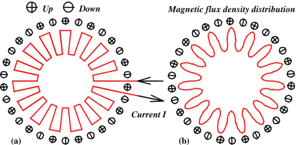
(36) Chapter 2 Design and fabrication. along different z directions.. Magnetic field directions. Up. Down. Magnetic flux density distribution. Current I. (a). (b). Magnetic pole pitch. Fig. 2-2. (a) Linear wire circuit pattern with a periodic structure. (b) The magnetic flux density distribution induced from the linear wire circuit pattern.. Annular wire circuit pattern is proposed and illustrated in Fig. 2-3 (a) to produce different magnetic fields in the radial direction. An annular multi-pole magnetic field distribution is obtained after applying a steady current to the annular wire circuit, as shown in Fig. 2-3 (b).. Consequently, a rotary type of multi-pole magnetic. component with a uniform pole profile is achieved. It is seen that the different multi-pole magnetic components with a uniform field distribution can be acquired without magnetization. Both of linear and annular wire circuit patterns can be easily fabricated on the PCB for different applications.. Up. Down. Magnetic flux density distribution. Current I (a). (b). Fig. 2-3. (a) Annular wire circuit pattern with a multi-pole configuration in the radial direction. (b) The magnetic flux density distribution induced from the annular wire circuit pattern.. 19.
(37) Chapter 2 Design and fabrication. Currently, the minimum wire width and the gap between any two adjacent wires on the circuit can be achieved about 3mils (~75µm, 1mil = 25.4µm) through the PCB manufacturing technology.. Accordingly, it is highly possible and feasible to. fabricate a multi-pole magnetic component with a fine magnetic pole pitch of less than 1mm.. A comparison among different methods in fabricating a multi-pole. magnetic component with a fine magnetic pole pitch is summarized on Table 2-1.. Table 2-1 Comparison among different methods Basic requirements Precise Magnetizing Magnetization Minimum Methods machining head machine pole pitch Conventional Yes Yes Yes ∼1mm magnetization Single-pulse Yes Yes Yes ∼100µm magnetization PCB manufacturing No No No ~150µm technology. Cost High Very high Low. Obviously, all precise machining technique, magnetizing head and magnetization machine are necessary in conventional and single-pulse magnetization methods. The manufacturing cost is thus very high and the minimum pitch sizes are around 1mm and 100µm, respectively. However, the innovative method of PCB manufacturing technology provides a simple process to fabricate a multi-pole magnetic component with a fine magnetic pole pitch, neither the precise machining technique nor the magnetizing head and magnetization machine is required. The magnetic pole pitch can be minimized to around 150µm. Although this pitch size is slightly larger than 100µm produced by using the single-pulse magnetization method, it has been significantly reduced to be smaller than 1mm. From above discussions, PCB manufacturing technology is not only a simple but also a feasible and convenient method to fabricate a multi-pole magnetic component with a fine magnetic pole pitch. Consequently, PCB manufacturing technology is 20.
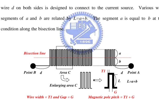
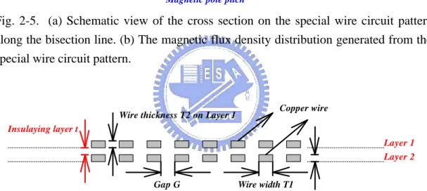
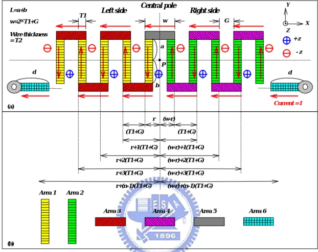
(38) Chapter 2 Design and fabrication. hired to narrow the magnetic pole pitch to be less than 1mm for this dissertation work. The detailed design and fabrication process will be discussed in the following sections.. 2.2 Design. A special wire circuit pattern was designed as in Fig. 2-4. All dimensions of wire segments on the circuit should be taken into account to obtain a desired pitch size. The spacing between any two adjacent wires is defined as the gap G.. The. sum of wire width T1 and gap G is defined as the magnetic pole pitch. A straight wire d on both sides is designed to connect to the current source. Various wire segments of a and b are related by L=a+b. The segment a is equal to b at the condition along the bisection line.. Bisection line. a b. Point B. d. T1. Area C. d L. Point A L=a+b. Enlarging area C G Magnetic pole pitch = T1 + G. Wire width = T1 and Gap = G. Fig. 2-4. Special wire circuit pattern designed for fabricating a multi-pole magnetic component with a fine magnetic pole pitch.. The schematic view of the cross section on the special wire circuit pattern along the bisection line is illustrated in Fig. 2-5 (a), indicating the wire thickness is T2. According to Ampere’s law, an alternate and regular magnetic field distribution is induced after applying a steady current to the wire circuit, as shown in Fig. 2-3 (b).. 21.
(39) Chapter 2 Design and fabrication. Thus, a multi-pole magnetic component with a fine magnetic pole pitch is obtained. Additionally, different pole numbers and pitch sizes can be also easily achieved by designing an appropriate wire circuit pattern.. (a). Wire thickness T2. Copper wire. Wire width T1 Gap G. Magnetic flux density distribution. (b). Magnetic pole pitch. Fig. 2-5. (a) Schematic view of the cross section on the special wire circuit pattern along the bisection line. (b) The magnetic flux density distribution generated from the special wire circuit pattern.. Wire thickness T2 on Layer 1. Copper wire. Insulaying layer t Layer 1 Layer 2 Gap G. Wire width T1 Wire thickness T2 on Layer 2. Fig. 2-6. Schematic view of the cross section on a dual-layered wire circuit structure along the bisection line.. A dual-layered wire circuit structure is considered to enhance the field strength in the fine magnetic pole pitch. Figure 2-6 shows the schematic view of the cross section on a dual-layered wire circuit structure along the bisection line.. The. geometrical structures of single-layered and dual-layered wire circuits are depicted in Fig. 2-7. An insulating layer t is inserted between two layers in the dual-layered wire circuit structure to prevent a short circuit. Both of Layer 1 and Layer 2 induce. 22.
(40) Chapter 2 Design and fabrication. the magnetic fields simultaneously after applying a steady current to the wire circuit. The total magnetic field is the sum of Layer 1 and Layer 2. Consequently, the field strength can be effectively enhanced using the dual-layered wire circuit structure. The large field strength in the wire circuit is useful to the signal detection. The details can be found in Chapter 5. Both of single-layered and dual-layered wire circcuit structures can be easily realized through the PCB manufacturing technology.. Layer 2. Wire width T1 Wire thickness T2. Layer 1 T2. T1. Insulating layer t. (a) Single-layered structure. Fig. 2-7. circuits.. (b) Dual-layered structure. Geometrical structures of (a) single-layered and (b) dual-layered wire. 2.3 Fabrication. 2.3.1 Drawing. First, the special wire circuit pattern with an appropriate layout must be designed and drawn by using drawing software such as AutoCAD, SolidWorks or Pro/E, etc. [28-30]. Here, AutoCAD is employed to do this job. In this step, the wire width, gap and corresponding position must be drawn and arranged accurately to acquire the desired pitch size and pole number. Various gaps of 150µm and 200µm with a wire width of 100µm are used to design 23.
(41) Chapter 2 Design and fabrication. different magnetic pole pitches of 250µm and 300µm on nine-pole magnetic components, as shown in Figs. 2-8 (a) and (b). The drawings of nine-pole magnetic components also have different fine magnetic pole pitches of 250µm and 300µm by using another wire width of 125µm with various gaps of 125µm and 175µm, as illustrated in Figs. 2-8 (c) and (d). Four holes located at corners are designed to fix the sample in measurements. Both of Point A and Point B are drawn for connecting to the current source.. Hole. gap = 150 um. Point B. Hole. Hole. Hole. Point A. 9 poles wire width = 100 um pole pitch = 250 um. gap = 125 um. Point B. Hole. Hole. (a). 9 poles wire width = 125 um pole pitch = 250 um. Hole. Point A. Hole. (c). Hole. gap = 200 um. Point B. Hole. Hole. Hole. Point A. 9 poles wire width = 100 um pole pitch = 300 um. gap = 175 um. Point B. Hole. Hole. (b). Hole. Point A. 9 poles wire width = 125 um pole pitch = 300 um. Hole. (d). Fig. 2-8. Various drawings of nine-pole magnetic components with different fine magnetic pole pitches of (a) 250µm by using a wire width of 100µm and a gap of 150µm, (b) 300µm by using a wire width of 100µm and a gap of 200µm, (c) 250µm by using a wire width of 125µm and a gap of 125µm, and (d) 300µm by using a wire width of 125µm and a gap of 175µm.. The circuit layout software such as OrCAD, Protel or PowerPCB, etc. can be used for the unit transformation to meet the specific requirement of PCB manufacturing process [31-33].. Here, PowerPCB is selected to proceed the assigned task. Several. standard file formats are acceptable for fabricating the wire circuit and the most. 24.
(42) Chapter 2 Design and fabrication. common is Gerber file format. The wire circuit patterns can be easily transferred to the substrate through using Gerber files.. 2.3.2 Wire circuit manufacturing process. Before starting the process, a mask with the special wire circuit pattern must be prepared by using Gerber files. cameras.. The mask is like a film used in conventional. Nine-pole and nineteen-pole wire circuit masks are demonstrated in Figs.. 2-9 (a) and (b), respectively.. (a). (b). Nine-pole wire circuit mask. Nineteen-pole wire circuit mask. Fig. 2-9 (a) Nine-pole and (b) nineteen-pole wire circuit masks.. The flow charts of wire circuit manufacturing process in fabricating the multi-pole magnetic component with a fine magnetic pole pitch is illustrated in Fig. 2-10 [34]. In the step (a), a copper film with a standard thickness is adhered to the surface of the substrate.. The surface of the copper film is very flat and its thickness can be. increased through an electroplating process. Usually the substrate material is made of glass epoxy (FR4) which has good electric and heat insulation. The surface of the copper film should be cleaned up to be free from dusts.. A photoresist layer is then. applied to the surface of the copper film in the step (b). The subsequent procedures are heating and curing the photoresist layer on the substrate. There are two kinds of photoresist, which are positive and negative.. The. positive photoresist will dissolve after light exposure and the negative photoresist will. 25.
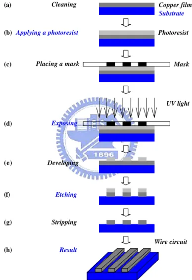
(43) Chapter 2 Design and fabrication. not. Here, the positive photoresist is selected to transfer the wire circuit pattern. The most popular method of coating the photoresist used in the process is so-called “Dry Film”. Using a hot roll laminator, the Dry Film can be laminated on the substrate and easily automated. Moreover, the Dry Film lamination is not sensitive to the cleanness, so this process is now popular for the fine wire manufacturing.. (a). Cleaning. Copper film Substrate. (b) Applying a photoresist. Photoresist. Placing a mask. Mask. (c). UV light (d). Exposing. (e). Developing. (f). Etching. (g). Stripping. (h). Result. Wire circuit. Fig. 2-10. Flow charts of wire circuit manufacturing process. (a) The surface of the copper film is cleaned up to be free from dusts. (b) A photoresist layer is applied to the surface of the copper film. (c) A pre-prepared mask is placed on the top of the photoresist layer. (d) The UV light is employed to proceed the light exposure process. (e) The non-exposed area is removed through a developing process. (f) The copper film at the exposed area is removed by chemical reaction using an etching solvent. (g) The residual photoresist on the surface of the wire circuit is stripped. (h) The wire circuit is accomplished on the substrate.. 26.
(44) Chapter 2 Design and fabrication. Subsequent steps of (c) and (d), a pre-prepared mask is placed on the top of the photoresist layer to proceed the light exposure process by using ultraviolet (UV) light. The special wire circuit pattern on the mask is transferred to the substrate after UV light exposure.. The wire circuit pattern is then formed from removing the. photoresist at the non-exposed area through the developing process (e).. In the. etching process (f), the copper film at the exposed area is removed by chemical reaction using an etching solvent such as ferric chloride, alkaline ammonia, cupric chloride, etc. The special wire circuit pattern is thus appeared on the substrate. Further steps of (g) and (h), the residual photoresist is stripped using a solvent so that a real wire circuit is accomplished on a substrate. A very thin thickness of gold (Au) is coated on the surface of copper wires to prevent oxidation.. Hole. Hole gap = 175 um. Point B. Point A. 9 poles wire width = 175 um pole pitch = 350 um. Hole. Fig. 2-11.. Hole. A nine-pole magnetic component fabricated on the PCB with a fine. magnetic pole pitch of 350µm by using a wire width of 175µm and a gap of 175µm.. A nine-pole magnetic component with a fine magnetic pole pitch of 350µm fabricated on the PCB by using a wire width of 175µm and a gap of 175µm is demonstrated in Fig. 2-11. Four holes located at corners are drilled in order to fix the sample for measurements. Two small holes inside Point A and Pont B are drilled as well to connect to the current source. All holes and shapes of wire circuit samples. 27.
(45) Chapter 2 Design and fabrication. are made through using CNC (computer numerical control) machine. Figure 2-12 shows another example of 29-pole magnetic component with a fine magnetic pole pitch of 500µm by using a wire width of 225µm and a gap of 275µm.. Hole. Hole gap = 275 um. Point A. Point B. 29 poles wire width =225 um pole pitch = 500 um. Hole. Fig. 2-12.. Hole. A 29-pole magnetic component fabricated on the PCB with a fine. magnetic pole pitch of 500µm by using a wire width of 225µm and a gap of 275µm.. 2.4. Summary. PCB manufacturing technology has been demonstrated to effectively narrow the magnetic pole pitch to be less than 1mm. This innovative method provides a simple process to fabricate the multi-pole magnetic component without using the complicated machining technique, magnetizing head and magnetization machine.. It is also a. cost-effective method to enable mass production easily. Additionally, different pole numbers and pitch sizes can be also easily fabricated on the PCB through this flexible approach.. 28.
(46) Chapter 3 Theoretical analysis. Chapter 3. Theoretical analysis. Several methods are applicable to compute the induced magnetic field in the fine magnetic pole pitch fabricated on the PCB due to the current input.. The field. distribution of a straight wire with a finite length can be easily acquired by using BiotSavart law.. The integral of magnetic flux density is evaluated numerically by. discretizing the volume into a mesh of elements. The wire circuit fabricated on the PCB can be treated as composed of many straight wires with a finite length that are located at different positions on the substrate. Consequently, the total magnetic flux density induced from the wire circuit can be obtained after accumulating the contribution of each straight wire.. All obtained field formulae in this chapter are. derived from a basic assumption of a uniform current density through the wire circuit.. 3.1 Long and straight wire. An element dl in a long and straight wire carrying a steady current I is shown in Fig. 3-1. According to Biot-Savart law, the magnetic flux density at the point P is. r µ I dl sinθ µ I dl cosα ˆ dB = 0 φˆ = 0 φ, 2 4π r 4π r 2. (3-1). where µ0 is the permeability of free space and φˆ is the unit vector in cylindrical r coordinates. The relative orientations of current I and magnetic flux density B. 29.
(47) Chapter 3 Theoretical analysis. satify the right-hand screw rule. Here. dα r 2 dα l = ρ tan α, ñ = r cos α, dl = ñ = . cos 2 α ñ. (3-2). Thus, from Eq. (3-1). r µ I +π µI B = 0 ∫ π 2 cosα dα φˆ = 0 φˆ. − 4πρ 2 2πρ. (3-3). r Lines of the magnetic flux density B are circles lying in a plane perpendicular to r the straight wire and centered on it. The magnitude of magnetic flux density B falls off as 1/ρ [36].. I ρ α. θ. l. dB. P φ. r. dl r. Fig. 3-1.. Long and straight wire carrying a steady current I, the element dl r contributes a dB at the point P.. 3.2 Straight wire with a finite length L. 3.2.1 Point P located outside the straight wire. An element dz’ in a straight wire with a finite length L carring a steady current I is 30.
(48) Chapter 3 Theoretical analysis. illustrated in Fig. 3-2. Wire segments of a and b are related by L=a+b, and the diameter of the straight wire is d.. I d. r >> d. dz' a z'. φ. R. dB. r. P (r,0,0). L O b. R = r 2 + z' 2. Fig. 3-2. A straight wire with a finite length L carrying a steady current I, the r element dz’ contributes a dB at the point P located outside the straight wire. r At the point P, the magnetic flux density dB is given by r r r r µ0 I dl × Rˆ ×R ˆ µ I d l dB = φˆ = 0 φ, 2 4π R 4π R 3. (3-4). and here. r r r r R = r 2 + z' 2 , dl = dz' zˆ, R = rrˆ− z' zˆ, dl × R = rdz'φˆ.. (3-5). The distance r is assumed r >> d. A special integration formula [37] is used to calculate Eq. (3-4) and it is. ∫. dx 2 32. (x ± a ) 2. =. 1 a2. ±x x2 ± a2. (3-6). .. 31.
(49) Chapter 3 Theoretical analysis. Thus, from Eq. (3-4) to Eq. (3-6). r µI B= 0 4π =. ∫. +a. −b. rdz' ( r + z' ) 2. 2. 3. 2. µI r φˆ = 0 2 4π r. a. z' z' +r 2. 2. φˆ −b. a b µ0 I + ( 2 )φˆ. 2 2 4πr a + r b + r2. a=b=L/2 I. (3-7). d. r >> d. dz'. φ. dB. a z'. R. L. Bisection line O P (r,0,0). r. b. R = r 2 + z '2. Fig. 3-3. A straight wire with a finite length L carrying a steady current I, the r element dz’ contributes a dB at the point P located along the bisection line of the straight wire.. 3.2.2 Point P loacted along the bisection line of the straight wire. The magnetic flux denisty at the point P located along the bisection line (a=b=L/2) of the straight wire in Fig. 3-3 can be calculated by Eq. (3-7) and given by. r µI B= 0 4π =. ∫. +a. −b. rdz' (r + z ) 2. 2. 3. 2. µI r φˆ = 0 2 4π r. z' z '2 + r 2. a. φˆ −b. L µ0 I a b 2 ˆ = µ0 I ( ( 2 + ) φ )φˆ. 2 2 2 2 2 4πr 2πr ( L ) + r a +r b +r 2. 32. (3-8).
(50) Chapter 3 Theoretical analysis. φ dB. I r >> d. P (r,0,h). d R. (h-z'). dz' L. (r,0,z'). z' r O. R = r 2 + (h - z ' ) 2. Fig. 3-4. A straight wire with a finite length L carrying a steady current I, the r element dz’ contributes a dB at the point P located at the upper position of the straight wire.. 3.2.3 Point P located at the upper position of the straight wire. The magnetic flux density at the point P located at the upper position of the straight wire in Fig. 3-4 can be obtained and here. r r R = r 2 + (h − z' ) 2 , dl = dz' zˆ, R = rrˆ+ (h − z' ) zˆ,. (3-9). r r dl × R = dz ' zˆ× [rrˆ + ( h − z ' ) zˆ] = rdz'φˆ.. (3-10). Thus, from Eq. (3-4). r µI B= 0 4π. ∫. µ I −r = 0 2 4π r. rdz'. L. 0. 2 32. [r + ( h − z ' ) ] 2. h − z' ( h − z' ) 2 + r 2. L. 0. µI φˆ = 0 4π. ∫. L. 0. − rd ( h − z' ) 2 32. [r + ( h − z ' ) ] 2. φˆ. µI h h− L φˆ = 0 ( − )φˆ. 2 2 2 2 4πr h + r ( h − L) + r. 33. (3-11).
(51) Chapter 3 Theoretical analysis. I d. r >> d r 2 + ( h + z ') 2. R=. dz'. r (r,0,z'). L z'. (h+z') R O. dB P (r,0,-h). φ. Fig. 3-5. A straight wire with a finite length L carrying a steady current I, the r element dz’ contributes a dB at the point P located at the lower position of the straight wire.. 3.2.4 Point P located at the lower position of the straight wire. The magnetic flux density at the point P located at the lower position (h=-h) of the straight wire in Fig. 3-5 can be aquired by Eq. (3-11) and given by. r µI B= 0 4π. ∫. µI r = 0 2 4π r. rdz'. L. 0. 2 32. [r + (h + z ' ) ] 2. L. h + z' (h + z ' ) + r 2. 2 0. µI φˆ = 0 4π. ∫. rd (h + z' ). L. 0. 2 32. [r + ( h + z ' ) ] 2. φˆ. µI h+L h φˆ = 0 ( − )φˆ. 2 2 2 2 4πr (h + L ) + r h +r. (3-12). 3.3 Two-dimensional analysis. Eq. (3-1) to Eq. (3-12) are derived from a hypothesis of the distance r >> d, and therefore the diameter d of the straight wire can be neglected in calculation. Howerver, the diameter d should be taken into account when r ≈ d .. The cross. section of a straight wire fabricated on the PCB is not circular but rectangular, which. 34.
(52) Chapter 3 Theoretical analysis. can be divided into a mesh of indexed elements, as shown in Fig. 3-6.. These. elements are equal in area containing the same amount of current density i.. I. i=. I. t1 =. T1. m1. T1 m1. t1. z'. dz'. a. φ. dB. Rn1. L O b. P (r,0,0). rn1 r. Rn1 = rn1 + z'2 2. r1 = ( r − 1 × t 1 ) r2 = ( r − 2 × t 1 ) r3 = ( r − 3 × t 1 ) rn1 = ( r − n1 × t 1). Fig. 3-6. Mesh of a straight wire with a finite length L carrying a steady current I and the wire width T 1 ≈ r . The distance rn1 decreases slightly with a small t1.. Here only the wire width T1 is taken into account and T 1 ≈ r . Each element is a straight wire with a finite length L.. Consequently, the induced magnetic flux density. can be calculated by Eq. (3-7). The integral of magnetic flux density is evaluated numerically by discretizing the surface into a mesh of indexed elements.. After. r summing the contribution of each element, the total magnetic flux density B produced by the straight wire at the point P is obtained and given by. r m1 µ i a b B=∑ 0 ( + )φˆ ( n1 = 1 ~ m1), 2 2 2 2 4 π r n 1=1 n1 a + rn1 b + rn1. 35. (3-13).
(53) Chapter 3 Theoretical analysis. where n1 is an interger, m1 is the “mesh” parameter that characterizes the discretization of wire width T1. Wire segments of a and b are related by L=a+b. Paramters of current density i and distance rn1 are given by. i=. I T1 , rn1 = ( r − n1 × t1), t1 = . m1 m1. (3-14). T1. Current Input I x. y. z 1 = ( z − 1 ×t2 ). T2. T1. rn1. z 2 = ( z − 2 ×t2 ). T2 Rn1, n2. z. a. z n2. z 3 = ( z − 3 ×t2 ). r θ. x. B z. P. z1 z 2 z3. Bz r1 = ( r − 1 ×t 1) r2 = ( r − 2 ×t 1). b. L=a+b (a). z. z n2. z n2 = ( z − n2 ×t 2) 2 2 Rn1,n 2 = rn1 + z n2. t1 t2. r3 = ( r − 3 ×t 1). T1 t1 = m1. rn1 = ( r − n1 ×t1 ). t2 =. T2 m2. (b). Fig. 3-7. (a) Mesh and (b) corresponding postions of all elements of a straight wire with a wire width T 1 ≈ r and a wire thickness T 2 ≈ r carrying a steady current I. The distances of rn1 and zn 2 decrease slightly with a small t1 and t2, respectively.. 3.4 Three-dimensional analysis. The wire thickness T2 also needs to be taken into account in calculation when T 2 ≈ r , as illustrated in Fig. 3-7 (a).. The integral of magnetic flux density in Eq. (3-. 7) can be evaluated numerically by discretizing the volume into a mesh of indexed elements. The corresponding positions of all elements are indicated in Fig. 3-7 (b). r. After summing the contribution of each element, the total magnetic flux density B 36.
(54) Chapter 3 Theoretical analysis. produced by the straight wire at the point P in the z direction is given by. Bz =. m1. m2. µ0i. ∑ ∑ 4πR. n1=1 n 2=1. a. ×(. a 2 + R n1,n 2. n1,n 2. 2. +. b b 2 + Rn1,n 2 2. ) × sinθ,. (3-15). where n1 and n2 are intergers, m1 and m2 are “mesh” parameters that characterize the discretization of wire width T1 and wire thickness T2, and θ is the angular offset of the X-axis. Wire segments of a and b are also related by L=a+b. Paramters of current density i, distance R n1,n2 and sin θ are. i=. I , Rn1,n 2 = rn1 2 + z n 2 2 , sinθ = rn1 , Rn1,n 2 m1 ⋅ m2. (3-16). and here. rn1 = ( r − n1 × t1), t1 =. T1 , m1. z n 2 = ( z − n 2 × t 2 ), t 2 =. (3-17). T2 , ( n1 = 1~m1, n 2 = 1~m2 ). m2. (3-18). 3.5 Field analysis. The wire circuit designed in Fig. 2-4 was redrawn as in Fig. 3-8 (a) in order to analyze the field distribution in the fine magnetic pole pitch. the current flow in the wire circuit.. The red arrows indicate. Various plus and minus marks denote the. induced magnetic field along different z directions. Both of wire width T1 and wire thickness T2 are taken into account simultaneously. The wire segment w is related. 37.
數據

+7
相關文件
GBytes 1024 MBytes P9-編號 2 資料磁區在 Linux 之作業系統
We explicitly saw the dimensional reason for the occurrence of the magnetic catalysis on the basis of the scaling argument. However, the precise form of gap depends
A diamagnetic material placed in an external magnetic field B ext develops a magnetic dipole moment directed opposite B ext. If the field is nonuniform, the diamagnetic material
A diamagnetic material placed in an external magnetic field B ext develops a magnetic dipole moment directed opposite B ext.. If the field is nonuniform, the diamagnetic material
reveal Earth’s magnetic field of the past?... The earth’s dipole field The
Define instead the imaginary.. potential, magnetic field, lattice…) Dirac-BdG Hamiltonian:. with small, and matrix
1. Infall guided by magnetic field, forming flattened envelope 2. Keplerian disk formed in flattened env. feeding protostar 3. Magnetic braking may reduce the disk size, if J
coordinates consisting of the tilt and rotation angles with respect to a given crystallographic orientation A pole figure is measured at a fixed scattering angle (constant d
