國 立 交 通 大 學
電 子 物 理 系
博 士 論 文
兆赫輻射波的產生與應用於釔鋇銅氧超導薄膜
特性之研究
Generation and Application of Terahertz Radiation in
Superconducting YBa
2Cu
3O
7-δThin Films
研 究 生 : 林博瑛
指導教授 : 吳光雄 教授
兆赫輻射波的產生與應用於釔鋇銅氧超導薄膜
特性之研究
Generation and Application of Terahertz Radiation in
Superconducting YBa
2Cu
3O
7-δThin Films
研 究 生 : 林博瑛 Student : Po-Iem Lin
指導教授 : 吳光雄 教授 Advisor : Prof. Kaung-Hsiung Wu
國 立 交 通 大 學 電 子 物 理 系
博 士 論 文
A Dissertation
Submitted to Department of Electrophysics College of Science
National Chiao Tung University in Partial Fulfillment of the Requirements
for the Degree of Doctor of Philosophy in Electrophysics October 2004 Hsinchu, Taiwan. 中華民國93 年 10 月
兆赫輻射波的產生與應用於釔鋇銅氧超導薄膜
特性之研究
研 究 生 : 林博瑛 指導教授 : 吳光雄 教授
國 立 交 通 大 學
電 子 物 理 系
中 文 摘 要
在本論文中,我們研究利用飛秒級超快雷射光激發半導體或高
溫超導體製作光致兆赫茲輻射脈衝產生源,且在國內外首次利用自由
空間電光取樣技術量取高溫超導薄膜在以飛秒脈衝雷射激發下,產生
之兆赫茲電磁輻射波的時域暫態波形。另外,由已建立之兆赫茲時域
頻譜量測分析技術,研究氧化物薄膜與基板材料在兆赫茲波段之時域
頻譜,以瞭解材料在此波段下之高頻電磁特性。
將半絕緣性之砷化鎵半導體微影蝕刻,鍍金後成為光導開關,
在外加偏壓下此光導開關受雷射光激發後,由於光電流隨時間的瞬
變,將產生高頻之兆赫茲輻射波,藉由利用自由空間電光取樣技術可
將此高頻輻射波形完整取出,經由快速傅力葉轉換可得一輻射頻譜分
佈。從改變不同的操作條件,我們已完整的研究分析利用半導體產生
兆赫茲輻射。利用不同的外加偏壓、超快雷射光的能量密度與光導開
關的孔隙大小,皆可獲得相同的兆赫茲輻射波形輸出。其頻率介於
dc 至 3 THz 之間。由此可知,利用光激發半導體產生高頻之兆赫茲
輻射波的輻射機制在上述之操作條件下是一致的。
在偵測方式上,我們以厚度
1 釐米的 ZnTe(110)電光晶體為偵
測器來感應兆赫茲輻射訊號。作用在
ZnTe 晶體上之兆赫茲輻射電場
強度與差分後之光電二極體所讀取到的信號有關。在我們的系統中,
兆赫茲輻射與探測光沿
ZnTe(110)面的法線分向傳播。隨著改變兆赫
茲輻射電場與探測光的偏振方向相對於晶體的
z 軸之夾角時,輻射場
強度大小和時域暫態波形的極性方向將會改變。當兆赫茲輻射電場與
探測光的偏振方向皆垂直於晶體的
z 軸時,可偵測到最大的強度值。
我們完成以釔鋇銅氧高溫超導薄膜作兆赫茲輻射源的特性量
測,包括改變不同雷射光能量、不同外加偏電流及不同量測溫度下之
兆赫茲時域瞬變波形。另外,薄膜在超導態時,超導載子會因外受輻
射光下,引起薄膜本身感應係數的變化,使得原來入射之輻射時域波
形會有再成形的現象。藉由適當的轉換函數,可模擬出輻射時域波形
的變化,並與實驗數據結果相符合。由結果顯示,光致超導體泰拉赫
茲輻射的機制是來自於超導電流密度隨時間的調變,從這些時間解析
量測所獲得的兆赫茲瞬間電場輻射波形,可以觀察到載子在非平衡狀
態下的動力行為。在超快雷射光激發下,超導電流密度變化量會先減
少,持續時間約為
1.0 ps;接續,超導電流密度變化量開始回升,持
續時間約為
2.5 ps,此回復時間大小和超導能隙是相關的。
另外,我們將使用半導體材料來產生兆赫茲輻射源,並且從已
建立之兆赫茲時域頻譜量測分析技術,研究氧化物薄膜與基板材料在
兆赫茲波段下之高頻電磁特性。利用量測結果與理論的分析比較,可
以獲到溫度與頻率相關之薄膜與基板材料之複數折射率,並進一步地
求得氧化物薄膜之介電係數、光導係數、穿透深度、準粒子的散射時
間等隨溫度、頻率的變化情形。
Generation and Application of Terahertz Radiation in
Superconducting YBa
2Cu
3O
7-δThin Films
Student : Po-Iem Lin Advisor : Prof. Kaung-Hsiung Wu
Department of Electrophysics
National Chiao Tung University
ABSTRACT
In this dissertation, three major parts are included. First, the observation of terahertz generation and detection from current-biased superconducting YBCO thin films excited by femtosecond optical pulses by using a free-space electro-optic sampling (FSEOS) technique is reported. The transient terahertz pulse was found to originate from the nonequilibrium superconductivity. Secondary, we also carried out systematic comparisons between the emissions generated with different operating parameters when using the semiconducting photoconductive switches as radiation source. Lastly, in relation to terahertz applications, we studied the terahertz frequency response in superconducting YBCO thin films by carrying out the terahertz time-domain spectroscopy (THz-TDS) measurements.
The characteristics of optically induced bipolar terahertz radiation in biased photoconductive switches and the emitted frequency spectrum distribution were found to remain unchanged even when the optical excitation fluence, strength of the biased field and the emitter gap spacing were varied. This suggests that the terahertz radiation obtained in the current setup must have originated from the same mechanism
which is believed to be associated with the ultrafast charge transport process during pulsed laser illumination.
On the other hand, the efficiency of terahertz detection strongly depends on the orientation of the terahertz polarization with respect to the ZnTe crystal (001) axis and on the angle between the polarization of the probe beam and that of the terahertz radiation. These results give the optimal operating parameters for terahertz pulse detection using the ZnTe sensor crystal.
The origin of photogenerated terahertz radiation pulse emitted from current-biased superconducting YBCOthin films excited by femtosecond optical laser pulses is delineated using a FSEOS technique. Picosecond electromagnetic pulses about 450 fs wide were obtained. The frequency spectrum derived by Fourier transforming the picosecond pulses spans over 0.1-4 THz. By investigating the performances of the transient terahertz radiation generated under different operating parameters, pulse reshaping in the measured terahertz electric field caused by the kinetic inductance of the superconducting charge carriers is identified. After recovering the original waveforms of the emitted terahertz pulses, the transient supercurrent density directly correlated to the optically excited quasiparticle dynamics is obtained. A fast decreasing component of about 1.0 ps and a slower recovery process with a value of 2.5 ps are unambiguously delineated in the optically induced supercurrent modulation. The radiation mechanism of the transient terahertz pulse related to nonequilibrium superconductivity is discussed.
Finally, we have used the established coherent terahertz time-domain spectroscopy technique to investigate the properties of the electrodynamics of
superconductor at terahertz frequencies. The temperature and frequency-dependent complex index of refraction of the materials, such as NdGaO3 substrate and YBCO
thin films, were determined by analyzing the complex transmittance. We used these analysis to explain the variation of the amplitude and phase of pulse shape of terahertz generation in current-biased YBCO thin film a FSEOS technique, and in observing the effect of pulse reshaping of terahertz transmission in YBCO thin films detected in the THz-TDS measurements. The temperature dependence of the real component of complex conductivity revealed a large broad peak over the whole measured terahertz range. It is attributed to a competition between an increase in the normal carrier relaxation time and a decrease in the number of normal carriers with decreasing temperature below Tc. By fitting the measured complex optical conductivity
) , ( T
ω
σ
with the aid of a two-fluid model, we were able to extract the temperature dependent of the London penetration depthλL(T)and the temperature dependence of致 謝
論文能夠順利完成,要感謝的人太多太多了。有大家的幫忙與扶持,才會 有今天的表現。首先要感謝指導老師吳光雄教授及研究群莊振益教授、林俊源教 授、溫增明教授、郭義雄教授耐心的指導與栽培。 另外,非常感謝口試委員清華大學齊正中教授、交通大學潘犀靈教授、清 華大學洪勝富教授以及中山大學周雄教授的指導與肯定。 實驗室裡裏的伙伴們,大家就像是一家人。雖然來自不同的地方,卻是有 緣共同在這兒相聚,名為”固態實驗室”。由於彼此相互的扶持與勉勵,生活六年 多以來的點點滴滴,不知不覺地在我的心中已然建造成一座城堡。老師們的指導 與教誨漸漸地使我成長與茁壯。在此感謝德峻學長、世溥學長、中裕學長、慧愷 學長、旭禎學長、世烽學長們在研究及生活上的相助與關懷。有志偉學弟的合作, 使得超快雷射光譜實驗室有了初步的雛型及成果。志昌學弟、璨耀學弟、維仁學 弟們如兄弟般的情感,義氣當頭,為了共同的目標而努力。感謝新山、雯妃、家 汶、宜蓁、美杏學弟妹們在實驗上的討論與幫忙。良星、彥瑞、佩君、峙文、育 全、維娟、瓊絹、東漢、沛宏、俐君、伯宗學弟妹們,有你們相伴,為我的研究 生涯增添色彩。 感謝珮雯多年來的體貼與照顧。在完成論文研究的這段時光,最需感謝的 是青慧的鼓勵,有妳的陪伴,讓我心中充滿了勇氣去面對未來。最後感謝的是我 最親愛的爸媽及兄弟們,有你們的支持與照顧,一路走來,始終無悔。Contents
Abstract (in Chinese) ………
ⅠAbstract (in English) ………
ⅣAcknowledgments ………
ⅦChapter 1 Introduction ………..
1Chapter 2 Preparation and Characterization Samples for Terahertz
Radiation Generation ………...
72.1 Characterization of superconducting YBa2Cu3O7-δ thin films deposited on MgO (100) substrate
……….
82.2 Fabrication of YBCO superconducting antenna as terahertz emitters
..
112.3 Fabrication of photoconductive switches as terahertz emitters
…
13Chapter 3 Generation and Detection of Terahertz Pulses ………...
143.1 Introduction
………...
143.2 Optical setup
………..
163.3 Bipolar photogenerated terahertz radiation in biased SI-GaAs photoconductive switches
………...
183.3.1 Origin of transient terahertz generation
……….
183.3.2 Optical fluence and biased voltage dependence
………..
193.3.3 Emitter gap spacing dependence
………..
233.4 Detection of terahertz pulses of FSEOS system
………...
263.4.1 Calculation of the refractive-index ellipsoid of the terahertz detection
………...
273.4.2 Orientation dependence of terahertz detection in ZnTe
…….
323.4.3 Transmission characteristics of terahertz detection in the optimum orientation of ZnTe crystal
………...
35Chapter 4 Characterization of Photogenerated Terahertz Radiation in
Current-Biased High-Tc Superconductor ………..
424.1 Introduction
……….
424.2 Experimental setup
………..
444.3 Photogenerated transient terahertz radiation
………..
464.3.1 Typical time profile and frequency spectrum of terahertz pulse
..
464.3.2 Polarity of the terahertz waveforms
………..
484.3.3 Radiation mechanism of superconductors
………..
484.4 Performances of transient terahertz radiation generated under different operating parameters
………
514.4.1 Optical excitation power dependence
……….
514.4.2 Biased current dependence
………....
534.4.3 Ambient temperature dependence
………..
564.5 The origin of photogenerated terahertz radiation emitted from current-biased superconducting YBa2Cu3O7-δ thin films
……
604.5.1 Kinetic inductance-induced pulse reshaping effect
……….
604.5.2 Temperature dependence of the original terahertz pulses from YBCO films
………...
654.5.3 Optically induced supercurrent modulation
…………..
674.6 Summary
……….
71Chapter
5
Terahertz Optical Conductivity of Superconducting
YBa
2Cu
3O
7-δThin Films ………
725.1 Principles of the terahertz time-domain spectroscopy
………
725.2 Theoretical treatment of the complex transmittance
………..
745.3 Experimental setup
………..
775.3.1 YBa2Cu3O7-δ thin films preparation
………
775.3.2 Optical setup of terahertz time-domain spectroscopy
….
795.3.3 Water vapor absorption in terahertz frequency region
…
815.3.4 Index reflection of NdGaO3 substrate in terahertz region
…
845.4 Optical conductivity in superconducting YBa2Cu3O7-δ thin films
…
885.4.1 Motivation
……….
885.4.2 Electrodynamics and the two-fluid model
………
895.4.4 The pulse reshaping effect in terahertz temporal profile
…
955.4.5 Optical constant and dielectric function
………..
965.4.6 Frequency and temperature dependence of complex optical conductivity spectra
………..
1005.4.7 Penetration depth and scattering rate
………...
1045.5 Summary
………...
107Chapter 6 Summary and conclusions ……….
108References ………
111Chapter 1
Introduction
Terahertz (THz) radiation, often called T-rays, loosely defined by the frequency range of 0.1 to 10 THz (1012 cycles per second), lies between infrared light and microwave radiation in the electromagnetic (EM) spectrum. There has been a revolution in terahertz systems in the past 20 years. Terahertz signals emanate from objects naturally, going through clothes, skin, plastics, cardboard, and semiconductors. Thus they enable a dizzying array of “X-ray vision” style application. For instance, terahertz signals naturally emanate from inside the human body, enabling X-ray-like imaging but without the side effects. What’s more, a terahertz scan could simultaneously analyze tissues to pinpoint abnormalities, like skin cancer, in the resulting 3-D model. Owing to the advanced materials research provided new and high-power terahertz sources, and the potential of terahertz for advanced physics research and applications was demonstrated [1-3]. In this terahertz gap, the last frontier in the EM spectrum, neither optical nor silicon solutions exist today. Most broadband pulsed terahertz generation are based on the excitation of different materials with ultrafast laser pulses. Photoconductive switching and optical
rectification are two of the most common approaches for generating pulsed terahertz beams.
The photoconductive technique is based on using high-speed photoconductors as transient current sources for radiation antennas [4,5]. Typical photoconductors include high-resistivity GaAs, InP and radiation-damaged silicon wafers. Metallic electrodes are used to bias the photoconductive gap and form an antenna. The optical rectification approach using electro-optic crystals as rectification media [6,7] is based on the process of the electro-optic effect. There, materials like ZnTe, GaAs, GaP and organic crystal have been chosen as the nonlinear medium. Recently, photoresistive devices based on the transient supercurrent density in high-temperature superconductor have been explored by several groups and can be considered as a useful manner to probe the nonequilibrium superconductivity with the femtosecond time-resolved spectroscopy [8,9].
Coherent terahertz radiation emitted from biased photoconductive switches has been extensively investigated [4,5,10]. In general, the externally biased constant voltage drives the photogenerated carriers to form a transient photocurrent across the field region. A radiated terahertz electric field is obtained by the time derivative of the net current. It acts as the source term in Maxwell’s equation, given as
t J ETHz ∂ ∂ ∝ → → ,
Eq. (1-1)
Terahertz emission from photoresistive devices, particularly, high-Tc
superconductors (HTSC), YBa2Cu3O7-δ (YBCO), has also been a topic of considerable
attention. It is possible to characterize the dynamics of Cooper pairs breaking and recombination. Also, HTSC devices show promise as high-speed optical detectors. However, understanding on the relaxation of photoexcited quasiparticles is required. The observation and detection of terahertz pulses emitted from optically excited
superconducting bridges have further revived the interest of using HTSC films as potential terahertz radiation sources [8,9,11,12]. Unfortunately, the radiation mechanism of photogenerated terahertz radiation in YBCO so far is still obscure because it is largely inconsistent with the characteristics of optically excited quasiparticle dynamics obtained by femtosecond time-resolved spectroscopy [13,14].
For pulsed terahertz detection, photoconductive sampling and free-space electro-optic sampling are the two most common methods. Fundamentally, the electro-optic effect is a coupling between a low-frequency electric field (terahertz pulse) and a laser beam (optical pulse) in the sensor crystal. Using a (110)-oriented Zincblende crystal as a sensor crystal; this in turn modulates the polarization ellipticity of the optical probe beam passing through the crystal. It is based on the Pockels effect in which an applied voltage causes the sensor crystal to become birefringent. The ellipticity modulation of the optical beam can then be analyzed to provide information on both the amplitude and phase of the applied terahertz electric field. Photoconductive sampling is widely used for pulsed terahertz detection. A similar structure to the photoconductive switches, with a gap in the center, may be used. Rather than applying a bias voltage to the electrodes of the switches, the transient terahertz field itself provides the bias voltage. As applying the terahertz field on the gap, carriers will move from one side of the antenna to the other. Finally, the current amplifier and meter are used to measure the transient current. The material used for the antenna is typically radiation-damaged silicon-in-sapphire or LT-GaAs, and has a very short carrier lifetime.
One breakthrough came in the form of a technique known as terahertz time-domain spectroscopy (THz-TDS), which was developed at Bell Laboratories in Murray Hill, New Jersey, in the mid-1990. The terahertz temporal waveform transmitted through the sample, for example a fresh leaf, can be analyzed in real time
to provide the information of the material’s characteristics [15]. Furthermore, THz-TDS allows a material’s far-infrared optical properties to be determined as a function of frequency. The Drude model may then be used to link to the material free-carrier dynamic properties, including the plasma angular frequency and the damping rate. HTSC characterization is another important application in terahertz fields. Owing to its unique capacity in uncovering the nonequilibrium superconductivity, particularly in YBCO, has been a topic of considerable attention in understanding the relaxation of photoexcited quasiparticles [3]. A new type of terahertz radiation imaging has been proposed [16]. The supercurrent distributions were visualized by detecting the radiation from optically excited HTSC. In addition, in THz-TDS applications, the superconducting thin films have been analyzed to determine material parameters including the magnetic penetration depth and scattering rate [17,18].
In 1990, Han et al. and Eesley et al. discovered the femtosecond dynamics of photogenerated quasiparticles in YBa2Cu3O7-δ superconducting thin films in
femtosecond time-resolved spectroscopy measurements [19-22]. Two main dynamic processes are involved: one is the avalanche multiplication of quasiparticle following photon absorption and the other one is the recombination of the quasiparticles to form Cooper pairs [8,23,24]. Recently, Demsar and Mihailovic et al. [13] further demonstrated that the photogenerated transient reflectivity change also consists of two distinct characteristic relaxation times in the superconducting state. In that the fast component dominantly occurred in subpicosecond range appears to be insensitive to temperature while the slow component in the range of several picosecond usually diverges near Tc, displaying signature of an energy gap opening [25,26].
From the application point of view, the pico- to subpicosecond relaxation back from nonequilibrium by recombination of the quasiparticles defines the principal
frequency limit of devices based on the dynamical changes of Cooper-pair densities. The typical nonequilibrium kinetic inductance photoresponse of voltage transient [27,28] was ascribed to the nonequilibrium quasiparticle generation and recombination in the presence of an applied dc bias current by using a subpicosecond electro-optic sampling technique [29,30]. The modulation of kinetic inductance by ultrafast laser pulses has been utilized recently as a sampling technique for measuring ultrafast electric waveforms [31]. On the other hand, the reshaping of terahertz pulses upon transmission through superconducting thin films caused by the kinetic inductance of the superconducting charge carriers was detected by using the coherent THz-TDS [32-36]. In general, the kinetic inductance of charge carriers in normal state can be neglected since the intrinsic impedance is usually dominated by the resistance in this regime. In superconducting state, however, the kinetic inductance becomes more significant and must be considered as an important parameter.
In this dissertation, in addition to investigating the origin of photogenerated terahertz radiation from current-biased superconducting YBCO thin films, we will focus specially on exploring dynamics in the far-infrared with THz-TDS technique [37-51]. Based on the analysis of THz-TDS measurements, one can directly, extract the complex index of refraction from the measured complex transmission of the superconducting thin film. In addition, the pulse reshaping effect in the measured terahertz temporal profile caused by the kinetic inductance of the superconducting charge carriers can be identified with the aid of a transmission line analog. The THz-TDS transmission measurements enable us to extract directly the temperature- and frequency-dependent complex optical conductivity, temperature-dependent London penetration depth, and the quasiparticle scattering time.
In what follows, the dissertation is composed of six chapters. In chapter 2, we introduce the fabrication and characterization of samples (both SI-GaAs and YBCO
thin films) to generate terahertz radiation.
Chapter 3 presents the characteristics of the optically induced bipolar terahertz radiation generated from biased SI-GaAs photoconductive switches and detected by using a free-space electro-optic sampling technique. The dynamics of the emitted terahertz transient is discussed. In addition, the orientation dependence of the terahertz detection in ZnTe (110) sensor crystal was analyzed to optimize the operation parameters for terahertz pulse detection.
In chapter 4, we present the characteristics of photogenerated terahertz radiation in HTSC. The results delineate clearly the origin of photogenerated terahertz radiation pulse emitted from current-biased superconducting YBCO thin films excited by femtosecond laser pulses. By taking into account the effect of the pulse reshaping caused by the kinetic inductance of the superconducting charge carriers, we demonstrate the direct connection between the quasiparticle dynamics and the detected terahertz radiation based on the supercurrent modulation.
In chapter 5, we describe the development of the THz-TDS technique and the applications of the means to investigate the properties of the electrodynamics of superconductors at terahertz frequencies. The temperature- and frequency-dependent complex index of refraction of the samples, such as NdGaO3 substrate and YBCO thin
films, are extracted by analyzing the complex transmittance. Besides, we are able to obtain the complex optical conductivity of the YBCO thin films due to the provided frequency-dependent information by the method of the THz-TDS.
Finally, in chapter 6, we give a summary of the prominent results discussed in this dissertation.
Chapter 2
Preparation and Characterization of Samples for
Terahertz Radiation Generation
In this chapter, we will present the sample preparation of two typical types of terahertz emitters SI-GaAs photoconductive switches and YBCO photoresistive devices. The characteristics of superconducting YBCO thin films deposited on MgO substrate were carefully studied. The films were then patterned into the antenna structure for further measurements. Meanwhile, pre-treatment of the MgO substrate prior to depositing YBCO thin film is necessary to improve the quality of films. The ultrafast photoresponse and quasiparticle relation dynamics of the YBCO films were measured by the femtosecond time-resolved spectroscopy.
2.1 Characterization of superconducting YBa
2Cu
3O
7-δthin films deposited
on MgO (100) substrate
MgO substrate is considered to be the ideal substrate for our purposes, since it remains transparent and non-dispersive at terahertz frequency measurements. Grischkowsky et al. reported that MgO is an excellent material in terms of its low loss and allows for the extended propagation of subpicosecond electromagnetic pulses at 85 K [52]. However, owing to the relatively large lattice mismatch between YBCO films and MgO substrate, quality of the epitaxial films depends substantially on the operating parameters including film’s deposition conditions and pre-treatment of the polished substrate [53,54]. As mentioned by Hsu et al. in our group [55], thermal annealing of the substrate is found to be highly effective in producing epitaxial c-axis films with good superconducting properties. The temperature is optimized such that sufficient structure mobility enables formation of a surface consisting of a series of steps [56,57]. This is partly due to the fact that the initial stage of YBCO growth on MgO substrates is predominantly by an island growth mechanism. It is, hence, highly favorable for these islands to nucleate at the edge of steps formed on the surface of the MgO (100) substrate. In our case, the MgO substrate was annealed at the temperature 1100 oC in 760 Torr of pure oxygen for 24 hrs.
YBCO thin films were deposited on 0.5-mm-thick MgO (100) substrates by conventional on-axis pulsed laser deposition (PLD) using a KrF excimer laser source with λ =248 nm operating at an energy density of 2.9 J/cm2. The substrate temperature was held at 750 oC and oxygen pressure was kept at 0.3 Torr during deposition. After deposition was completed, oxygen gas was introduced into the PLD chamber to 1 atm, and was cooled down to room temperature. The films with a typical thickness of 110 nm were c axis oriented. The transport properties of typical
0 30 60 90 120 150 180 210 240 270 300 0 3 6 9 12 YBCO/MgO
Resistance (
Ω
)
Temperature (K)
Tc=88 KFIG. 2-1 Resistance versus temperature curve for typical YBCO thin film grown on MgO (100) substrate. The substrate has been thermal annealing previously.
temperature dependent resistance curve of YBCO thin film measured by standard four-probe method is illustrated in Fig. 2-1. The film exhibits good metallic behavior with a critical temperature Tc of about 88 K after it annealing separately at the temperature 450 oC in 760 Torr of pure oxygen for 30 min.
The real-time measurements of the relaxation dynamics of YBCO superconducting films was investigated by using the femtosecond time-resolved spectroscopy. Usually, the optical reflectivity measured by the optical pump-probe method has the time scale ranging from few hundred femtosecond to picosecond range. While the gap opening is manifested by a rapid increase in the amplitude of the
-2 0 2 4 6 8 10 12 14 10 20 30 40 50 0 2 4 6 8 10 1 10 τ 2 ~ 2.3 ps τ1 < 1 ps Time Delay (ps) ∆ R/ R ( 1 0 -5 ) T=60 K
Time Delay (ps)
∆
R/R (10
-5)
FIG. 2-2 Optical response of a YBCO thin film after excitation with fs laser pulses at 60 K. The inset shows reflectivity transient ∆R /R with time on a logarithmic scale. The solid line is drawn to indicate the trend. Here, the 300-nm-thick YBCO film was deposited on SrTiO3 (100) substrate for optical measurements [58].
photogenerated transient reflectance in the superconducting state as illustrated in Fig. 2-2, the relaxation apparently consists of two time scales. The ultrafast rise of the reflectivity after photoexcitation of the YBCO is attributed to quasiparticle generation (including the Cooper pairs breaking and photoexcitation of lower energy quasiparticles), and the subsequence decrease of the reflectivity results from quasiparticle relaxation mainly limited by recombination to Cooper pairs. The higher energy quasiparticles will relax to the lower energy quasiparticles via emitting phonons or quasiparticles; meanwhile, the lower energy quasiparticles could also recombine to form the Cooper pairs [14].Within this scenario, two distinct characteristic relaxation times in the superconducting state have been identified. Below Tc, as shown in the inset of Fig. 2-2, the logarithmic plots of ∆R /R reveal a break in slope near t=2.5 ps. Two relaxation processes [13,14] (fast component τ1
and slow component τ2) in our measured data can be clearly observed in YBCO films. In this case, the two-component fit to the data yields two relaxation times with
1
τ ~0.7 ps and τ2~2.3 ps at 60 K. The slow relaxation component τ2 of ∆R /R is considered to relate to the superconducting gap.
2.2 Fabrication of YBCO superconducting antenna as terahertz emitters
The as-deposited YBCO thin films were then patterned into a bow-tie antenna structure using standard photolithography and wet chemical etching. The critical temperature Tc (at R=0) remained 88 K after patterning into the antenna structure showing practically no shift in critical temperature comparing to the original film. Figure 2-3 displayed the configuration of the antenna that the center bridge is 200
μm long and 100μm wide with the bow-tie angle of 60 o. Where, low resistivity electrical contacts to the film were made by evaporating approximately 200-nm-thick gold pads on the YBCO surface, which were subsequently annealed in 760 Torr of pure oxygen at 450 oC for 30 min [59].
Regarding to the electric properties of YBCO antenna, the I-V characteristic was shown in Fig. 2-4 which the critical current density Jc was about 1.7*106 A/cm2 at 77 K. we note that the film grown on the polished substrate typically exhibit a Jc
FIG. 2-3 Configuration of bow-tie
antenna structure of YBCO thin films (dark area) deposited on MgO substrate. The locations of god pads were displayed in square region. The optical pulses will incident normal to the center bridge of YBCO antenna.
-2.0x10⁻⁴ -1.0x10⁻⁴ 0.0 1.0x10⁻⁴ 2.0x10⁻⁴ -40 -20 0 20 40 YBCO/MgO Tc=88 K Jc=1.7*106 A/cm2 at T=77 K Ic=27 mA (1 µV criterion)
I (m
A
)
V (Volt.)
FIG. 2-4 I-V characteristic taken at 77 K of antenna fabricated in a YBCO thin
film.
(9.7*104 A/cm2) which is slightly smaller than that of films deposited on the annealed substrate (2.3*105 A/cm2 at 84 K), indicating the significant enhancement of transport properties by step-mediated growth.
2.3 Fabrication of photoconductive switches as terahertz emitters
We also chose undoped semiconductor material (SI-GaAs wafer) to fabricate the emitters of terahertz radiation. The thickness of the high resistivity wafer (
ρ
>10k Ω-cm) is about 0.35 mm for the highly efficient terahertz propagation. The Au/Ge metal patterns of about 150-nm-thick used as electrodes are obtained by standard lift-off procedures. Figure 2-5 illustrated the layout of the fabricated photoconductive switches. A DC voltage bias was applied across the emitter, and the pump beam was normally incident. Characterization of the gap spacing of emitters was achieved by pattering the geometry. One can take the semiconductor material as the ideal photoconductive switch to generate terahertz radiation not only for understanding the fundamental properties of pulse shape of radiation but also employing in the study of the electrodynamics of superconductors analyzed by the terahertz time-domain transmission spectroscopy.The characteristics of terahertz pulses generated from the YBCO photoresistive switches and SI-GaAs photoconductive switches will be presently and discussed in chapter 3 and 4, respectively.
500μm , 100 μm , 10 μm SI-GaAs Au Vdc fs Laser 500μm , 100 μm , 10 μm SI-GaAs Au Vdc fs Laser
FIG. 2-5 Schematic illustration
of the top view of the SI-GaAs photoconductive switches.
Chapter 3
Generation and Detection of Terahertz Pulses
3.1 Introduction
Broad-band coherent terahertz (THz) radiation emitted from biased photoconductors after excitation by an ultrafast laser pulse [60-63] has been used as a spectroscopic tool for characterizing carrier transport in semiconductors [64,65], examining gap and subgap features of superconductors [66,67], and for the emerging applications of coherent terahertz imaging [68]. The emitted terahertz waveforms and frequency spectrum of the biased photoconductive switches have been studied by several groups [65,69]. Under some particular conditions, bipolar terahertz waveforms were obtained both in large- and small- aperture photoconductive switches. Usually, both large- and small-aperture photoconductive switches are defined to have an optically illuminated area of dimensions comparable to the center wavelength of the emitted radiation. The mechanism of the photoinduced terahertz radiation, however, is still a matter of debate. For instance, the reason why the emitted waveforms can exhibit unipolar and bipolar characteristics has provoked some exotic interpretations
[69]. In order to clarify some of the controversial issues, it is of interest to carry out systematic comparisons between the emissions generated with different operating parameters.
In this chapter, terahertz radiations obtained from biased photoconductive switches with various emitter gap spacings, applied bias fields and optical excitation fluences are reported. Our results showed that with the gap spacing ranging from 10 to 500 µm, the emitted radiations are all bipolar in nature. Furthermore, the waveform and the frequency spectrum distribution do not depend on the optical excitation fluence or strength of the biased field. This suggests that the terahertz radiation obtained in the current setup originates from essentially the same mechanism as that associated with the ultrafast charge transport process during pulsed laser illumination.
Depending on the radiation and detection schemes employed, the resultant waveforms and frequency bandwidths were different and had been a subject of extensive research. For instance, Cai et al. [70] and Park et al. [71] have made a direct comparison between the performances and detected waveforms of free-space electro-optic sampling and photoconductive antenna detection schemes to detect coherent terahertz radiation emitted from biased low-temperature-grown GaAs emitters.
In terahertz detection measurements, we use a free-space electro-optic sampling (FSEOS) system to observe the transient terahertz radiation from the semi-insulating GaAs (SI-GaAs) photoconductive switches. The polarization change of the probe beam occurs when the ZnTe sensor crystal, based on the Pockels effect, is irradiated by the terahertz electric field. The terahertz-induced phase retardation of the probe beam is converted into an intensity modulation and detected by using balanced photodiodes. Picosecond electromagnetic pulses will be obtained. Besides, the orientation dependence of the terahertz detection in ZnTe was analyzed to optimize
the operation parameters for terahertz pulse detection.
The FSEOS system can also be used to measure the characteristics of terahertz radiation generated from the photoconductive materials and to study the nonequilibrium processes in high-Tc superconductors. Furthermore, based on the set up of technique of terahertz generation and detection, we can establish coherent terahertz time-domain spectroscopy technique, which uses SI-GaAs photoconductive switch as the terahertz radiation source, to measure the high frequency response such as the temperature- and frequency-dependent of the index of refraction, optical conductivity, and penetration depth in HTSC films. These results will be presented in chapter 4 and 5.
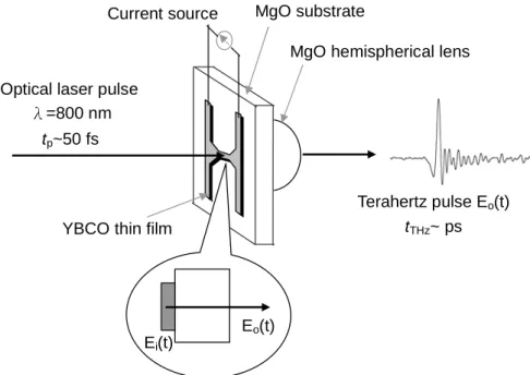
3.2 Optical setup
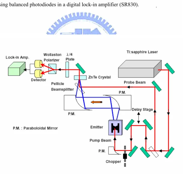
The experimental setup of the free-space electro-optic sampling system [68,72] is illustrated schematically in Fig. 3-1. A CW argon-laser-pumped, compact mode-locked Ti:sapphire laser (femtosource C20) provides 20 fs optical pulses at 800 nm (1.55 eV) with a 75 MHz repetition rate. The pump beam aligned at normal incidence is modulated by a mechanical chopper operated at 1.3 kHz. The electric field of a terahertz pulse is sampled by scanning the delay between the pump and probe beam. An undoped SI-GaAs photoconductive emitter, triggered by femtosecond laser pulses, radiates the THz beams. The emitted radiation is collimated and focused by a pair of off-axis paraboloidal mirrors onto the ZnTe sensor crystal. The Au/Ge metal patterns of the planar emitters are obtained by standard lift-off procedures. A
FIG. 3-1. Schematics of the experimental setup of free-space electro-optic sampling
system.
5-µm-thick pellicle beam splitter, which is transparent to the terahertz beam, is used to reflect 50% of the synchronized optical probe beam collinearly along the terahertz beam. The polarized terahertz and probe beams are aligned to a 1-mm-thick <110>-oriented ZnTe sensor crystal. We used a quarter-wave plate to impart a π/2 optical bias to the probe beam, which allows the system to be operated in the linear range. A Wollaston polarizer is used to convert the terahertz-field-induced phase retardation of the probe beam into an intensity modulation between the two mutually orthogonal linearly polarized beams. The optical intensity modulation is detected using balanced photodiodes in a digital lock-in amplifier (SR830).
Pump
beam
THz
radiation
Bias
Emitter
Pump
beam
THz
radiation
Bias
Emitter
500μm , 100 μm , 10 μm SI-GaAs Au Vdc fs Laser 500μm , 100 μm , 10 μm SI-GaAs Au Vdc fs Laser3.3 Bipolar photogenerated terahertz radiation in biased SI-GaAs
photoconductive switches
3.3.1 Origin of the transient terahertz generation
In general, when a femtosecond laser pulse illuminates the semiconductors with a photon energy greater than the band gap (for SI-GaAs, band-gap Eg=1.42 eV), photons are absorbed, thus creating electrons and holes. The external biased field drives the photogenerated carriers to form a transient photocurrent across the field region. Namely, a radiated terahertz electric field is obtained by the time derivative of the net current. It acts as the source term in Maxwell’s equations.
t J ETHz ∂ ∂ ∝ , Eq. (3-1) By biasing a constant voltage across the gap spacing of the emitter, carriers photoinjected into the gap by ultrafast laser pulse will be accelerated, leading to the emission of a transient and broad-band frequency terahertz radiation [Fig. 3-2].
FIG. 3-2. Schematics of terahertz
generation as a femtosecond laser pulses illuminates the biased photoconductive switches. The gap spacing of emitters is illustrated in the lower panel.
-2 0 2 4 -3 -2 -1 0 1 2 3 4 5 6
×
130 1×
(b) (a) 130mW 1mWElectric Field (arb. units)
Time Delay (ps)
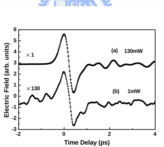
FIG. 3-3. Transient terahertz waveforms for 500 µm gap spacing photoconductive
switches. The average pumping power is (a) 130 mW and (b) 1 mW.
3.3.2 Optical fluence and biased voltage dependence
Figure 3-3 shows the typical photogenerated terahertz signals as a function of the scanning delay time obtained from the SI-GaAs photoconductive switches with a biased field of 2 kV/cm. The average pumping powers (fluences) are (a) 130 mW (0.8
µJ/cm2) and (b) 1 mW (60 nJ/cm2). The gap spacing of this emitter is 500 µm.Nearly symmetrical terahertz waveforms are observed. The signal-to-noise ratio (SNR) is about 103 (106 in power) for the 130 mW case. In contrast, for the 1 mW case, strong noise is observed before delay time t=0. There are some secondary peaks not shown here that appeared after about 15 ps delay of the main terahertz signals, which are believed to arise from substrate multiple reflections.
-2 0 2 4 6 -1.0 -0.5 0.0 0.5 1.0
Electric Field (arb. units)
Time Delay (ps)
Photocurrent Transient(arb. units)
FIG. 3-4. Time integral of the measured terahertz electric field of SI-GaAs
photoconductive switches. The induced photocurrent produced and vanished with a time of about 2.1 ps.
In Fig. 3-3, an integrated terahertz pulse is sampled about 2 ps. The time integral of the measured terahertz electric field of SI-GaAs photoconductive switches shown in Fig. 3-4 will be separated into two parts: the rise time and the fall time components. The rise time (the full width of half-maximum (FWHM) is 310 fs) and fall time of the photocurrent are 0.9 ps and 1.2 ps, respectively. The induced photocurrent produced and vanished with a time of about 2.1 ps. The carrier transient time across the biased field width is obviously much shorter than the carrier lifetime (~100-300 ps). This cannot be explained by attributing the effects to carrier lifetime as was proposed by Budiarto et al [73].
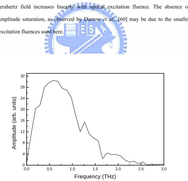
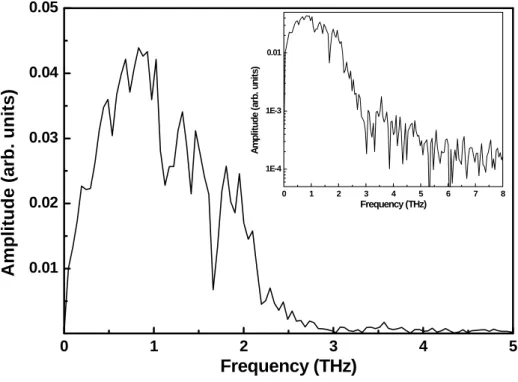
0.0 0.5 1.0 1.5 2.0 2.5 3.0 0 4 8 12 16 20 24 28 32 Frequency (THz)
Amplitude (arb. units)
FIG. 3-5. Corresponding frequency spectrum by Fourier transform of the terahertz
waveforms.
Figure 3-5 shows the representative power spectrum derived by Fourier transform of the terahertz waveforms. The radiation frequency spectrum extends from 0.1 THz to 3 THz. The central frequency is 0.7 THz and the region of maximum intensity distribution of the spectral pattern lies in the range of 0.4~0.9 THz. The bandwidth of half-maximum (BWHM) of the frequency spectrum is around 1.1 THz. Fig. 3-6 shows plots of a series of emitted bipolar terahertz radiations as a function of average pumping power for the 0.5-mm-wide photoconductive switch. It is evident that the symmetrical terahertz waveforms remain intact over the whole range of optical excitation fluences studied. Moreover, the peak strength of the emitted terahertz field increases linearly with optical excitation fluence. The absence of amplitude saturation, as observed by Darrow et al., [60] may be due to the smaller excitation fluences used here.
-1.0
-0.5
0.0
0.5
1.0
1.5
-3
-2
-1
0
1
2
3
130mW
100mW
50mW
25mW
10mW
1mW
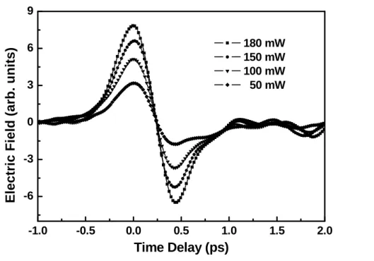
FIG. 3-6. The figure shows a series of emitted terahertz waveforms obtained at
various average pumping powers for 500 µm gap spacing photoconductive switches.
-1.0 -0.5 0.0 0.5 1.0 1.5 2.0 -6 -3 0 3 6 9
Electric Field (arb. units)
Time Delay (ps)
180 mW 150 mW 100 mW 50 mW
FIG. 3-7. A series of emitted transient terahertz waveforms for 10-µm-wide
3.3.3 Emitter gap spacing dependence
From the above results, it is evident that, in large-aperture photoconductive switches, the bipolar nature of the terahertz radiation waveforms is independent of pumping power. It is thus interesting to see whether the waveforms and frequency spectra would change with the emitter gap spacing. Fig. 3-7 shows a series of emitted bipolar terahertz radiations as a function of average pumping power for the 10-µm-wide photoconductive switch. As can be seen, the slightly unsymmetrical terahertz waveforms remain intact over the whole range of optical excitation fluences studied. Nearly the same ratio of the terahertz pulse for the positive lobe to that for the negative lobe is obtained under different optical excitation fluences for a 10 µm emitter gap spacing. For 100 µm gap spacing photoconductive switches (not shown here), similar behaviors are also observed. Since the size of the laser spot is about 500
µm and 30 µm for 500 µm and 10 µm gap spacing switches, respectively, the current
results display no signature of unipolar to bipolar waveforms transitions [65].
Since the waveforms are essentially the same for all cases, it is suggested that the broad-band frequency spectrum of the emitted radiation is not dependent on either the excitation fluences or the emitter gap spacing. In addition, experiments have shown that the waveforms and frequency spectrum of the emitted radiation display no dependence on the strength of the biased field. In our measurement configuration, the optical pumping (800 nm) is incident normal to the emitter substrate so that the radiation output is independent of surface depletion and different frequency mixing due to the surface χ(2) of photoconductors. [74] The robust characteristics of the emitted radiation indicate that the same underlying physical mechanism prevails in all cases.
In fact, similar results have been reported by Lu et al. [68] for a 2.5-mm-wide emitter using the free-space electro-optic sampling technique. These, however, are in sharp contrast with some of the results reported in literature. It has been proposed that bipolar waveforms of terahertz radiation, which can only appear in large-aperture photoconductors with high optical excitation fluences, are a consequence of space-charge screening of the bias field. [69] On the other hand, Pederson et al. [65] studied the effects of carrier density on the emitted waveform for a 50-µm-wide emitter and concluded that the emitted radiation changes from unipolar to bipolar with increasing photoexcited carrier density. In our case, a bipolar nature of terahertz radiation is obtained, and the fall time of the transient photocurrent seems to be independent of the different operating parameters. In other words, the carrier transient time across the biased field width, in either the 500-µm- or 10-µm-wide photoconductive switches, is very fast and much shorter than the carrier lifetime. Since the bipolar nature of the terahertz radiation obtained in the current setup persists in virtually every case studied, the current results can be interpreted consistently in terms of the mechanism associated with the ultrafast charge transport process during pulse laser illumination. The apparent discrepancies mentioned above may arise merely from detection and sampling techniques. It is noted that the alignment for the generation and detection of terahertz radiation must be handled very carefully for the 10 µm gap spacing emitter in the experimental process. The laser spot of focused optical normal incidence may partly pass through the substrate and be detected by the system at higher fluences. Such a situation may have blurred the actual signals from the photogenerated radiation.
In conclusion, the characteristics of optically induced bipolar terahertz radiation in biased photoconductive switches were investigated systematically by a free-space electro-optic sampling technique. It was observed that the bipolar nature
and the emitted frequency spectrum distribution remained unchanged on varying the optical excitation fluence, strength of the biased field and the emitter gap spacing. These results are in agreement with the dynamics of the optically induced ultrafast charge transport driven by the biased field.
FIG. 3-8. Free-space electro-optic sampling
3.4 Detection of terahertz pulses of FSEOS system
Developed originally for the characterization of ultrashort electrical transients, the electro-optic sampling (EOS) reported by Zhang et al., [see Fig. 3-8] as developed into a powerful method of the detection of terahertz pulses [72]. The EOS is based on the electric field of a terahertz pulse inducing an instantaneous birefringence in an electro-optic crystal through a non-linearity of the first order (Pockels effect). Passing through such crystal, the initially linearity polarized optical probe beam gains small elliptical polarization. The starting point of the calculation of the terahertz detection is the refractive-index ellipsoid that arises when an electric field is applied to the crystal. Since the terahertz pulse is much longer than the laser pulse (several ps versus tens of fs), the terahertz pulse can be approximately treated as a dc bias field. Thus, by varying the delay between terahertz- and optical probe pulses the whole time profile of the pulse can be traced.
E
p y (010)k
p z (001)k
THz α ψ x (100)E
THz ZnTe (110) crystal3.4.1 Calculation of the refractive-index ellipsoid of the terahertz detection [75,76] The orientation of the 1-mm-thick <110>-oriented ZnTe crystal with respect to the propagation direction and polarization of the terahertz and optical probe beam is shown in Fig. 3-9. kTHz and kp give the propagation directions of the terahertz and the probe beam, respectively. We define α as the angle of the terahertz beam polarization with respect to the (001) axis (z axis) and
ϕ
as the angle of the probe beam polarization with respect to the crystal (001) axis. The index ellipsoid defines the refractive index in the crystal that is experienced by visible-near-IR light propagating through the crystal with a given propagation direction and polarization. With no electric field applied, the material (ZnTe) is isotropic so that the refractive-index ellipsoid is simply a sphere i.e. ni,j =n for every i and j. The coordinate system x’, y’, and z’ is linked to the propagating beams: the beams travel along the x’=<-1,-1,0> direction, the optical probe and the terahertz beams are polarized with an angle respect to the crystal (001) axis. Under the influence of the applied terahertz field, the sphere [Fig. 3-10(b)] turns to an ellipsoid [Fig. 3-10(c)] with the main oriented along x”, y”, and z” directions [Fig. 3-10(a)].FIG. 3-9. Relative orientation of
the terahertz electric field and the polarization of the laser probe-and the terahertz beams with respective to the ZnTe crystal. kTHz
and kp give the propagation
directions of the terahertz and the probe beam, respectively. x corresponds to the (100) axis, y to the (010) axis, and z to the (001) axis.
FIG. 3-10. (a) The refractive-index ellipsoid. The x, y, z coordinates are set along
the main ZnTe crystallographic direction; the primed axes are defined as the terahertz- and the optical probe beams propagation(x’), the terahertz- and the probe beams(z’=z) polarization directions. The double-primed axes correspond to the orientation of the main axes of the refractive-index ellipsoid under the terahertz field applied. (b) and (c) depict the projection of the ellipsoid on the surface of the crystal (i.e. as it is seen by the incident laser probe beam): without the terahertz field (b) and with terahertz field present (c).
Its optical properties can be described with the refractive-index ellipsoid 1 2 2 2 2 2 2 = + + n z n y n x , Eq. (3-2) where x, y, and z define the coordinate axes in the crystal, with the z axis corresponding to the (001) crystal axis. Now, if a terahertz field is applied to the crystal, the electric field would modify the refractive index of the crystal. This is so
(a)
called electro-optic effect and the Eq. (3-2) of index ellipsoid can be modified to Eq. (3-3) where
γ
41 ( 3.9 10 12m /V 41 − × =γ
) is the electro-optic coefficient [77]. 1 2 2 2 , 41 , 41 , 41 2 2 2 2 2 2 = + + + + + E yz E xz E xy n z n y n x z THz y THz x THzγ
γ
γ
, Eq. (3-3) where ETHz,x, ETHz,y, and ETHz,z are the components of the applied terahertz field ETHz along the x, y, and z directions, respectively, and where n is the unperturbed refractive index. The presence of the mixed terms yz, xz, and xy in Eq. (3-3) indicates that the axes of the ellipsoid do not coincide with the coordinate axes. The main problem is to find a coordinate transformation such that the main axes of the ellipsoid are aligned with the new coordinate axes. Then, by projecting the probe-laser polarization on these axes, we can calculate the effect that the field-induced refractive-index change has on the pulse polarization as it propagates through the crystal. We can make an immediate simplification by noting that, for a terahertz pulse propagating along the (110) axis, ETHz,y = -ETHz,x. After studying Eq. (3-3), we find that we need two coordinate transformations to align the index ellipsoid with the new coordinate axes. The first transformation is a rotation of 45o around the z axis,' ' ' ' 2 1 2 1 45 sin 45 cos y x y x x= o − o = − , ' ' ' ' 2 1 2 1 45 cos 45 sin y x y x y = o + o = + , Eq. (3-4) ' z z= ,
Equations (3-4) transform the ellipsoid into the form
1 2 2 ) 1 ( ) 1 ( ' ' 41 , 2 2 ' 41 , 2 2 ' 41 . 2 2 ' + + − + + E yz = n z E n y E n x THzz
γ
THzzγ
THzxγ
, Eq. (3-5) From the remaining mixed y term in Eq. (3-5) we deduce that a final 'z'rotation of the (x',y',z') system with the x' axis is needed to align the coordinate
system with the main axes of the index ellipsoid. Taking the angle over which the coordinate system is rotated to be
θ
, we can write for the transformation" ' x x = ,
θ
θ
sin cos " " ' y z y = − , Eq. (3-6)θ
θ
cos sin " " ' y z z = + ,We express the components of the electric field in terms of the angle α:
α
cos ,z THz THz E E = , α sin 2 1 ,x THz THz E E = , Eq. (3-7) with ETHz =|ETHz|. With these definitions and after some algebra, we find for the index ellipsoid(
)
[
]
(
)
[
cos cos cos 2]
11 2 cos sin cos 1 cos 1 2 41 2 2 " 2 41 2 2 " 41 2 2 " = ⎭ ⎬ ⎫ ⎩ ⎨ ⎧ − − + + ⎭ ⎬ ⎫ ⎩ ⎨ ⎧ − + + + ⎟ ⎠ ⎞ ⎜ ⎝ ⎛ +
θ
α
θ
α
γ
θ
α
θ
α
γ
α
γ
THz THz THz E n z E n y E n x Eq. (3-8) in which cosαsinθcosθ +sinα(cos2θ −sin2θ)=0provided that α θ 2tan 2 tan =− Eq. (3-9)
(
α)
π θ =−arctan 2tan −n 2π
α
π
⎟ ⎠ ⎞ ⎜ ⎝ ⎛ + < ≤ ⎟ ⎠ ⎞ ⎜ ⎝ ⎛ − 2 1 2 1 n n , n=0,1,…The angle θ over which we rotate the coordinate system around the axis x' is thus
a function of the angle α between the terahertz polarization and the (001) axis. This ellipsoid can be alternatively be written as
1 2 " 2 " 2 " 2 " 2 " 2 " = + + z y x n z n y n x , Eq. (3-10)
For small electric fields, 2 41ETHz <<1 n/
γ , we obtain from Eq. (3-8) the refractive indices for visible-near-IR light propagating along the x"direction
[
cos sin cos( 2 )]
2 ) ( 2 41 3 " α ≈ + THzγ α θ + α + θ y E n n n ,[
cos cos cos( 2 )]
2 ) ( 2 41 3 " α ≈ + THzγ α θ − α + θ z E n n n , Eq. (3-11) where θ is given by Eq. (3-9).
Figure 3-10 shows the curve formed by the interaction of the plane perpendicular to the direction of propagation (i.e. as it is “seen” by the incident laser probe beam) with the index ellipsoid. For the case in which no terahertz field is applied, the curve has the form of circle [Fig. 3-10(b)], showing that the refractive index has the value n for any direction of polarization. For the case in which a terahertz field is applied, this curve has the form of an ellipse [Fig. 3-10(c)]. Consequently the semiminor and semimajor axes of this ellipse are along the y and "
"
z direction and have lengths n and y" n respectively. z"
A wave polarized in the y direction propagates with a different phase "
velocity than a wave polarized in the z direction. In propagating through the length "
of the modulator crystal, the y and " z polarization components will thus acquire "
the phase shift Γ :
[
n n]
L c L n c ( ) y"(α
) z"(α
)ω
ω
∆ = − = Γ , Eq. (3-12) where L is the crystal length. We get[
α θ α θ]
γ ω 2 sin sin 2 2 cos cos 2 41 3 − = Γ c L E n THz , Eq. (3-13) which is known as the retardation. In the absence of the terahertz field (ETHz=0), the phase shift is zero and the polarization of the probe beam stays linear. When, however, the terahertz pulse is present the phase shift Γ leads to a slightly elliptical polarization.From Eqs. (3-11) and (3-13) it is clear that ny" and n are different and z"
the y and " z direction, the probe field becomes elliptically polarized. The "
intensity difference, ∆I, of the polarization components that correspond to the ellipse can be calculated [75]:
[
]
[
]
⎭ ⎬ ⎫ ⎩ ⎨ ⎧ − − = ∆ n n L c II(
α
,ϕ
) psin 2(ϕ
θ
) sinω
y"(α
) z"(α
) , Eq. (3-14) where L is the crystal length, Ip, is the probe intensity, c is the velocity of light in vacuum, and ω is the angular frequency of the probe pulse. When the field-induced phase difference is small, we can replace the second sine in Eq. (3-14) with its arguments. Using Eq. (3-9) and relation (3-11), we can then simplify the equation to) 2 cos sin 2 2 sin (cos 2 ) , ( 41 3 ϕ α ϕ α γ ω ϕ α = + ∆ c L E n I I THz p , Eq. (3-15) Equation (3-15) shows that the signal from the balanced detectors is proportional to the applied electric field. Thus, by the variation of the delay between terahertz- and optical probe pulses the whole time profile of the terahertz pulse can be traced.
3.4.2 Orientation dependence of terahertz detection in ZnTe
Equation (3-15) indicated the measured dependence on the crystal’s azimuthal angle α of the detected terahertz electric field between the probe beam polarization and the terahertz polarization. Interestingly, a comparison of the maximum signals between the terahertz polarization and the probe beam polarization shows that the maximum signal is obtained for ϕ =α +90o or
ϕ
=α
[75]. Thus, in our case,α
ϕ
= , we get ) 2 cos sin 2 2 sin (cos 2 ) ( 41 3 α α α α γ ω α = + ∆ c L E n I I THz p , Eq. (3-16)FIG. 3-11. The measured pulse shapes of the terahertz pulses with respect to the crystal’s azimuthal angle
α
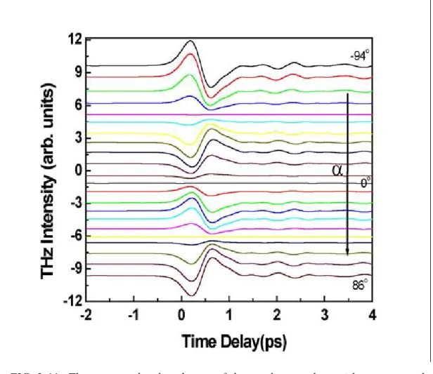
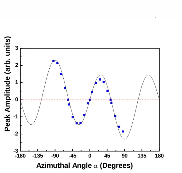
.The measured results of the terahertz pulses with respect to the crystal’s azimuthal angle α is illustrated in Fig. 3-11. The terahertz pulse shape keep unchanged, but the intensity of the signal and the polarity will vary with the angle α. Figure 3-12 shows the measured maxima of the terahertz amplitude as a function of the azimuthal angle α when the probe beam polarization is parallel to the terahertz
beam polarization. As α =ϕ =90o, in our case, we can get the maxima signal
c L E n I I THz p 41 3 ) , (α ϕ = ω γ ∆ , Eq. (3-17) The orientation dependence of terahertz beam detection in ZnTe was accomplished by using an undoped SI-GaAs photoconductive switch [78]. The
-180 -135 -90 -45 0 45 90 135 180 -3 -2 -1 0 1 2 3
Azimuthal Angle
α
(Degrees)
Pe
ak Amplitude (arb.
units
)
FIG. 3-12. The measured maxima of the terahertz amplitude as a function of the (110)-oriented ZnTe crystal’s azimuthal angle α when the probe beam polarization is parallel to the terahertz beam polarization, where the terahertz measurements (square) and fit curve [Eq. (3-16)] (solid line).
calculation is based on Eq. (3-16) and is in excellent agreement with the measurements, showing the correct maxima and minima in the terahertz detection efficiency as a function of the azimuthal angle [see Fig. 3-12]. These results show the optimal operating parameters for terahertz pulse detection using the ZnTe crystal.
3.4.3 Transmission characteristics of terahertz detection in the optimum orientation of ZnTe crystal
Here, we will focus on the calculation of the refractive-index ellipsoid of the terahertz radiation as operating in the optimal parameters. From the results of the Fig. 3-12, one can measure maxima intensity of the terahertz signal as the angles satisfiedα =ϕ =90o. The polarization of both the terahertz and optical probe beams are aligned parallel to the [1,-1,0] direction of (110) oriented ZnTe sensor crystal. The ellipsoid of the Eq. (3-5) will then rewritten as
1 2 ' ' 41 2 2 ' 2 2 ' 2 2 ' = + + + E yz n z n y n x THzγ Eq. (3-18) where, , = cos90o =0 THz z THz E E and o THz THz y x E E E E =− =(1/ 2) sin90 =(1/ 2) .
In addition, from the Eq. (3-9), the angle θ of the second coordinate transformation is obtained of value 45o. From the remaining mixed y'z' term in Eq.
(3-18) we deduce that a final rotation of the (x',y',z') system with the x' axis is
needed to align the coordinate system with the main axes of the index ellipsoid. Taking the angle over which the coordinate system is rotated to be
θ
=45o, we can write for the transformation" ' x x = , " " " " ' 2 1 2 1 45 sin 45 cos z y z y y = o − o = − , Eq. (3-19) " " " " ' 2 1 2 1 45 cos 45 sin z y z y z = o + o = + ,
Equation (3-19) transform the ellipsoid into the form 1 ) 1 ( ) 1 ( "2 2 41 41 2 2 " 2 2 " = − + + + THzγ ETHzγ n z E n y n x , Eq. (3-20) Equation (3-20) shows that "x ,y", and z"are indeed the principal axes of the