The proximity of the strain induced effect to improve the electron mobility in a
silicon-carbon source-drain structure of n-channel metal-oxide-semiconductor
field-effect transistors
E. R. Hsieh and Steve S. Chung
Citation: Applied Physics Letters 96, 093501 (2010); doi: 10.1063/1.3340926
View online: http://dx.doi.org/10.1063/1.3340926
View Table of Contents: http://scitation.aip.org/content/aip/journal/apl/96/9?ver=pdfcov Published by the AIP Publishing
Articles you may be interested in
Rare-earth oxide/TiN gate stacks on high mobility strained silicon on insulator for fully depleted metal-oxide-semiconductor field-effect transistors
J. Vac. Sci. Technol. B 29, 01A903 (2011); 10.1116/1.3533760
Carrier transport in strained N-channel field effect transistors with channel proximate silicon-carbon source/drain stressors
Appl. Phys. Lett. 97, 032111 (2010); 10.1063/1.3465661
Strained Si, SiGe, and Ge channels for high-mobility metal-oxide-semiconductor field-effect transistors J. Appl. Phys. 97, 011101 (2005); 10.1063/1.1819976
Secondary ion mass spectrometry characterization of source/drain junctions for strained silicon channel metal–oxide–semiconductor field-effect transistors
J. Vac. Sci. Technol. B 22, 327 (2004); 10.1116/1.1640659
Electron mobility enhancement in strained SiGe vertical n-type metal–oxide–semiconductor field-effect transistors
Appl. Phys. Lett. 78, 377 (2001); 10.1063/1.1342038
This article is copyrighted as indicated in the article. Reuse of AIP content is subject to the terms at: http://scitation.aip.org/termsconditions. Downloaded to IP: 140.113.38.11 On: Wed, 30 Apr 2014 11:57:00
The proximity of the strain induced effect to improve the electron mobility
in a silicon-carbon source-drain structure of n-channel
metal-oxide-semiconductor field-effect transistors
E. R. Hsieh and Steve S. Chunga兲
Department of Electronics Engineering and Institute of Electronics, National Chiao Tung University, Hsinchu 300, Taiwan
共Received 7 November 2009; accepted 8 February 2010; published online 4 March 2010兲 The source/drain in an n-channel metal-oxide-semiconductor field-effect transistor 共nMOSFET兲 with solid phase epitaxial共SPE兲 implanted Si:C before the spacer formation is proposed. Compared to the conventional nMOSFET with SPE implanted Si:C after the spacer formation, it brings in proximity to the device channel and shows great improvement of electron mobility via the stronger tensile strain effect. Experimental measurements showed that the electron mobility in the proposed process is increased by 105% over that of the control devices. At a gate length of 40 nm, an increase of more than 67% for the drain current, comparing to those of the conventional Si:C source/drain nMOSFET, has been achieved. © 2010 American Institute of Physics.关doi:10.1063/1.3340926兴
In order to extend the scaling of complementary metal-oxide semiconductor 共CMOS兲 transistors while keeping good performance,1,2 the enhancement of carrier mobility making utilization of strain-induced effect is one of the promising approaches.3In more recent years, different tech-niques have been employed for n- and p-channel metal-oxide-semiconductor field-effect transistor 共nMOSFET/ pMOSFET兲, with an attempt to provide flexible tuning of the strain effects in terms of design and manufacturing purposes.4–10In p-MOSFET, hole mobility can be boosted by the usage of silicon-germanium共SiGe兲 stressor in the source/ drain共S/D兲,4–7which induces uniaxial compressive-strain ef-fect into the channel, via the lattice-mismatch induced strain between the interface of SiGe S/D and silicon channel re-gions. On the other hand, in nMOSFET, silicon-carbon 共Si:C兲 in S/D with an induced tensile-strain effect becomes feasible as a counter part of pMOSFET in the CMOS structures.4,8–10
More recently, there are three mainstream technologies to adopt the carbon-dopant to form the Si:C in the S/D, in-cluding solid phase epitaxy 共SPE兲,11 SPE implantation,12,13 and in situ doping.14 The electron mobility, eff,
enhance-ment based on embedded Si:C in the S/D structure is highly dependent on the carbon concentration共C%兲 of Si:C and the strength of tensile strain in the channel. As a result of the low solid dissolubility of carbon in silicon, many groups paid a lot of efforts on how to increase C% of Si:C,11–14 however, the improvement would be limited by the carbon out-diffusion since it makes the device reliability worse for a high dopant.8In the aforementioned processes, SPE process shows lower substitutional carbon concentration共e.g., about ⬃1%兲.2
SPE implantation shows higher C% of 1.65%;9 in addition, the position and concentration of C% in this pro-cess are more adjustable than the others. However, the an-nealing steps are involved after carbon implantation, which could release the tensile strain in the channel and adversely degrade the performance. In order to avoid this strain-released effect, in situ doping process was demonstrated.13It
shows C% of 2.1%, but the consequence is the concern of carbon out-diffusion.
In this work, by using the SPE implantation, Si:C in the S/D extension region was prepared. Before spacer formation, S/D region was shallowly recessed with dry etching. Then, Si:C epilayer was selectively formed in the S/D region with 1.15⫻1015 cm−2of carbon, implanted together with Arsenic
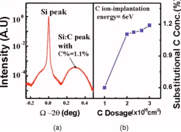
doping. Si:C was completed by using a low temperature 共950 °C兲 SPE process, and meanwhile, dopant was also ac-tivated at the same SPE step. Since SPE process is a low temperature process, the lateral diffusion of S/D extension during anneal is very limited comparing to the conventional activation process, in which the latter tends to give longer lateral diffusion as a result of high temperature thermal bud-get using either laser spike anneal or rapid thermal process that has been commonly used for the annealing of S/D. The substitutional carbon concentration 共C%兲 of Si:C, 1.1%, is examined by the x-ray diffraction共XRD兲 spectrum as shown in Fig. 1共a兲, in which the lower concentration 共1.1%兲 is
a兲Electronic mail: [email protected].
FIG. 1. 共Color online兲 共a兲 The XRD measurement of the Si:C films. The effective substitutional C dopant concentration is 1.1%. 共b兲 The ion-implanted C condition: C% = 1.1% at C dosage= 2⫻1015 cm−2and energy = 6 keV. Note that the substitutional C dopant tends to saturate with in-creasing carbon dosage.
APPLIED PHYSICS LETTERS 96, 093501共2010兲
0003-6951/2010/96共9兲/093501/3/$30.00 96, 093501-1 © 2010 American Institute of Physics
This article is copyrighted as indicated in the article. Reuse of AIP content is subject to the terms at: http://scitation.aip.org/termsconditions. Downloaded to IP: 140.113.38.11 On: Wed, 30 Apr 2014 11:57:00
resulting from the annealing steps after carbon ion-implantation. To improve the C% of Si:C and to achieve abrupt carbon profile, low temperature and ultrashort anneal-ing temperatures were employed 共temperature=950 °C and time⬍1 ms兲. The condition of substitutional carbon concen-trations dependent on ion-implanted carbon impurities is also demonstrated in Fig.1共b兲. It was observed that the substitu-tional carbon concentration tends to saturate when ion-implanted carbon dosage is larger than 2⫻1015 cm−2, as a
result of the very low solid dissolubility of carbon in the silicon. As a consequence, we faced the difficulties to in-crease C% further because when annealing temperature is raised to increase C%, the tensile strain will be released; when the carbon dosage is increased, the C% is easy to be saturated. Therefore, it is hard to increase the dopants共C%兲 of Si:C further.
To enhance the tensile-strain effect into the channel and to avoid the dilemma as described above, the SPE implanta-tion of the carbon impurity is introduced into the S/D exten-sion region共S/D-E兲 instead of that in the S/D region. Figure 2共a兲shows major steps of the fabrication process. Figure2共b兲 shows the cross sections with two different structures, namely,共i兲 Si:C in the S/D extension region, and 共ii兲 Si:C in the S/D region. First, active regions with threshold-voltage 共Vth兲 tuning are defined, and then polysilicon gate,
oxy-nitride gate insulator, S/D extension implantation, silicon ni-tride spacer, and S/D implantation are formed in sequence. For both processes, carbon impurity ion-implantation and an-nealing steps are utilized to form Si:C, since the SPE implan-tation could be integrated easily into S/D-E 共or S/D兲 before 共or after兲 the spacer formation. The processing steps 共i兲 in Fig.1共a兲provide the modified SPE implantation process with Si:C stressor in the S/D-E region, and steps 共ii兲 are the standard12SPE implantation process with Si:C stressor in the S/D region.
The strength of the strain in the channel is very sensitive to the geometry effect and the manufacturing process, so the simulation needs to consider these factors. The simulation work was performed by Synopsys SentaurusTCAD
共Technol-ogy Computer Aided Design兲 software,15 in which those stress mechanisms associated with the materials, i.e., stresses
induced by the growth of materials, densification, thermal mismatch, and lattice mismatch, were used. For a Si:C S/D uniaxial stressor in n-channel transistor, Sxxis required to be
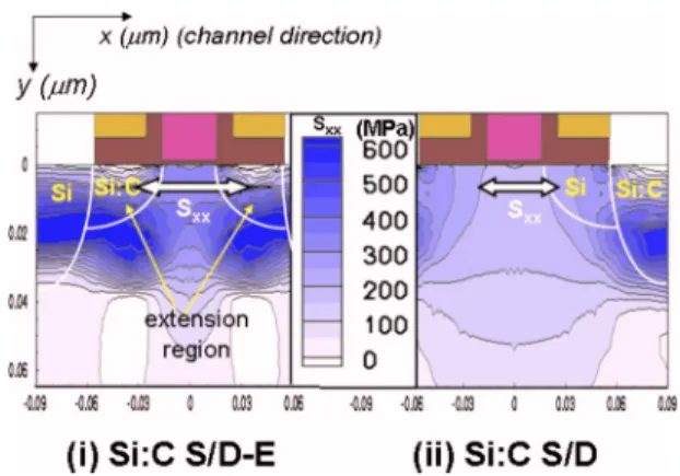
tensile strain to enhance the electron mobility.1,4Figures3共a兲 and 3共b兲 show the simulated profiles of longitudinal tensile stress共Sxx兲 for the conventional Si:C in S/D region 共Si:C S/D
device兲 and the Si:C in S/D extension region 共Si:C S/D-E device兲. These simulated results considered all device inte-gration processes 共including thermal activation processes兲 and took into account the integration between carbon and S/D 共or S/D-E兲 dopants. The strength of Sxxis larger in the
proximity of the stressor and decreases far away from the stressor along the channel direction; thus, the smallest inten-sity exists in the middle of the channel. It is because the lattice-mismatch on the interface of Si:C and silicon will release the strain which decays with the increasing distance. As a result, in order to enlarge the magnitude of Sxx, we have
to bring the proximity of strain effect through the stressor more close to the channel. For the comparison in Fig. 3, it can be seen that Sxx for the Si:C S/D-E process introduces
strain effect more close to the channel共the darker area show-ing a higher strain effect兲, comparshow-ing to the conventional Si:C S/D ones. Additionally, the substitutional carbon con-centration共C%兲 of Si:C S/D-E process is higher than that of Si:C S/D process thanks to a lighter dopant interference in the area below the S/D extension junction, where the con-centration of S/D dopant is low.
Figure4共a兲shows the calculated effective mobility,eff, versus the effective electric field characteristics for the Si:C S/D-E device, Si:C S/D device, and the control device, re-spectively. It reveals a fairly large improvement in the mo-bility enhancement of 105% for the Si:C S/D-E device in comparison to that of the control device. The larger the strength of tensile-strain in channel is, the more enhancement of mobility for the carriers in the channel becomes. This proposed structure has the merit of inducing more strain to the channel while keeping a low C% of Si:C effectively. In short, with the improvement of longitudinal tensile stress 共Sxx兲 in the channel, the effective mass and the scattering
events of electrons have been reduced, which gives rise to a higher effective mobility in Si:C S/D-E structures. Results in Fig.4共b兲show the IDS-VDScharacteristics of nMOSFET with
a gate length of 40 nm for both Si:C S/D-E device, SiC S/D device, and the control device at the same operating bias,
FIG. 2.共Color online兲 Key process sequences for the fabrication of strained nMOS devices. 共a兲 New process 共i兲 SPE implanted C before the spacer formation for nMOSFET with Si:C in the S/D extension region, and con-ventional process 共ii兲 SPE implanted C after the spacer formation for nMOSFET with SiC in S/D region.共b兲 The cross sectional views for process 共i兲 and process 共ii兲 in 共a兲. The differences are the formation of SiC before and after the spacer formation.
FIG. 3. 共Color online兲 The simulated longitudinal stress 共Sxx兲 along the channel direction, for共i兲 Si:C S/D-E devices and 共ii兲 Si:C S/D process. It can be clearly seen that the intensity of the strain in共i兲 Si:C S/D-E process is higher and more close to the channel共darker area兲 in comparison to the conventional Si:C S/D ones共ii兲.
093501-2 E. R. Hsieh and S. S. Chung Appl. Phys. Lett. 96, 093501共2010兲
This article is copyrighted as indicated in the article. Reuse of AIP content is subject to the terms at: http://scitation.aip.org/termsconditions. Downloaded to IP: 140.113.38.11 On: Wed, 30 Apr 2014 11:57:00
VDD= 1V + Vth. The Si:C S/D-E device shows ID,sat 共at VDS
= VDD+ Vth兲 improvement of 67% over that of the control device.
In conclusion, to have a trade-off between the carbon out-diffusion and the strength of the tensile strain in the channel for a certain design of Si:C S/D structure, the use of Si:C underneath the gate-drain overlap region is an excellent candidate for fabricating high electron mobility nMOSFETs. The induced tensile-strain has been in proximity to the chan-nel which results in a higher electron mobility. Experimental measurements showed that the electron mobility in the pro-posed process is increased by ⬃105% over that of the con-trol devices, and the IDS-VDScharacteristics show the benefit
of 67% over that of the control devices at the same operating bias. In addition, the Si:C S/D-E process still keeps low C%, which can reduce thermal budget and prevent the carbon out diffusion which might hurt the device reliability.
The authors would like to thank the team of Central R&D Division, UMC, Taiwan for wafer fabrication used in
this study. This work was supported in part by the National Science Council, under the Contract No. NSC96-2221-E009-185.
1S. E. Thompson, G. Sun, Y. S. Choi, and T. Nishida,IEEE Trans. Electron
Devices 53, 1010共2006兲.
2S. E. Thompson and S. Parthasarathy,Mater. Today 9, 20共2006兲. 3Y. Sun, S. E. Thompson, and T. Nishida, J. Appl. Phys. 101, 104503
共2007兲.
4K.-W. Ang, K.-J. Chui, V. Bliznetsov, C.-H. Tung, A. Du, N. Balasubra-maniam, G. Samudra, M. F. Li, and Y.-C. Yeo, Appl. Phys. Lett. 86,
093102共2005兲.
5P. R. Chidambaram, C. Bowen, S. Chakravathi, C. Machala, and R. Wise,
IEEE Trans. Electron Devices 53, 944共2006兲.
6K. Mistry, M. Armstrong, C. Auth, S. Cea, T. Coan, T. Ghani, T. Hoff-mann, A. Murthy, J. Sandford, R. Shaheed, K. Zawadzki, K. Zhang, S. Thompson, and M. Bohr, Dig. Tech. Pap. - Symp. VLSI Technol. 2004, 50.
7S. S. Chung, D. C. Huang, Y. J. Tsai, C. S. Lai, C. H. Tsai, P. W. Liu, Y. H. Lin, C. T. Tsai, G. H. Ma, S. C. Chien, and S. W. Sun, Tech. Dig. - Int. Electron Devices Meet. 2006, 325.
8S. S. Chung, E. R. Hsieh, D. C. Huang, C. S. Lai, C. H. Tsai, P. W. Liu, Y. H. Lin, C. T. Tsai, G. H. Ma, S. C. Chien, and S. W. Sun, Tech. Dig. - Int. Electron Devices Meet. 2008, 435.
9K.-W. Ang, K.-J. Chui, V. Bliznetsov, A. Du, N. Balasubramaniam, G. Samudra, M. F. Li, and Y.-C. Yeo, Tech. Dig. - Int. Electron Devices Meet.
2004, 1069.
10S. S. Chung, E. R. Hsieh, P. W. Liu, W. T. Chiang, S. H. Tsai, T. L. Tsai, R. M. Huang, C. H. Tsai, W. Y. Teng, C. I. Li, T. F. Kuo, Y. R. Wang, C. L. Yang, C. T. Tsai, G. H. Ma, S. C. Chien, and S. W. Sun, Dig. Tech. Pap. - Symp. VLSI Technol. 2009, 158.
11Y.-C. Liu, O. Gluschenkov, J.-H. Li, A. Madan, A. Ozcan, B. Kim, T. Dyer, A. Chakravarti, K. Chan, C. Lavoie, I. Popova, T. Pinto, N. Rovedo, Z. Luo, R. Loesing, W. Henson, and K. Rim, Dig. Tech. Pap. - Symp. VLSI Technol. 2007, 44.
12Z. Ren, G. Pei, J. Li, B. Yang, R. Takalkat, K. Chan, G. Xia, Z. Zhu, A. Madan, T. Pinto, T. Adam, J. Miller, A. Dube, L. Black, J. W. Weijtmans, B. Yang, E. Harley, A. Chakravarti, T. Kanarsky, R. Pal, I. Lauer, D.-G. Park, and D. Sadana, Dig. Tech. Pap. - Symp. VLSI Technol. 2008, 172. 13B. Yang, R. Takalkar, Z. Ren, L. Black, A. Dube, J. W. Weijtmans, J. Li, J. B. Johnson, J. Faltermeier, A. Madan, Z. Zhu, A. Turansky, G. Xia, A. Chakravarti, R. Pal, K. Chan, A. Reznicek, T. N. Adam, B. Yang, J. P. de Souza, E. C. T. Hariey, B. Greene, A. Gehring, M. Cai, D. Aime, S. Sun, H. Meer, J. Holt, D. Theodore, S. Zollner, P. Grudowski, D. Sadana, D. G. Park, D. Mocuta, D. Schepis, E. Maciejewski, S. Luning, J. Pellerin, and E. Leobandung, Tech. Dig. - Int. Electron Devices Meet. 2008, 51. 14H.-S. Wong, K.-W. Ang, L. Chan, K.-M. Hoe, C.-H. Tung, N.
Balasubra-manian, D. Weeks, M. Bauer, J. Spear, S. G. Thomas, G. Samudra, and Y.-C. Yeo,IEEE Electron Device Lett. 29, 460共2008兲.
15TCAD Sentaurus user manual共Synopsys, Version C, 2009兲. FIG. 4.共Color online兲 共a兲 Plot of the effective mobility vs effective electric
field which shows an increase of 105% for SiC S/D-E device over the control device.共b兲 Plot of IDvs VGSfor gate length= 40 nm, showing the enhancement of driving currents with over 67% increase in Si:C S/D-E device over the control device, while conventional Si:C S/D just shows an increase of 10%.
093501-3 E. R. Hsieh and S. S. Chung Appl. Phys. Lett. 96, 093501共2010兲
This article is copyrighted as indicated in the article. Reuse of AIP content is subject to the terms at: http://scitation.aip.org/termsconditions. Downloaded to IP: 140.113.38.11 On: Wed, 30 Apr 2014 11:57:00