Nitrogen Implantation and In Situ HF Vapor Clean for Deep
Submicrometer n-MOSFETs
Jiann Heng Chen,aTan Fu Lei,a,zChia Lin Chen,bTien Sheng Chao,b
Wen Ying Wen,cand Kuag Ting Chenc
a
Department of Electronics Engineering and Institute of Electronics, National Chiao Tung University, Hsinchu, Taiwan
b
National Nano Device Laboratory, Hsinchu, Taiwan cWinbon Electronics Corporation, Hsinchu, Taiwan
This work describes a high performance and reliable deep submicrometer n-channel metal oxide semiconductor field effect transistor共n-MOSFET兲 with ultrathin gate oxide prepared by combining nitrogen gate electrode implantation and native-oxide-free in situ HF vapor preoxidation cleaning. The results herein reveal that the performance and reliability, including the leakage current of the ultrathin gate oxide, charge-to-breakdown, drain current, transconductance, charge pumping current, stress induced leakage current, and hot carrier reliability of n-MOSFETs are all significantly improved. The enhanced reliability and performance are attributed to the native-oxide-free process, smooth interface, and reduced incorporation of As in the gate oxide which results from HF vapor cleaning and nitrogen implantation.
© 2001 The Electrochemical Society. 关DOI: 10.1149/1.1421607兴 All rights reserved.
Manuscript submitted February 15, 2001; revised manuscript received July 15, 2001. Available electronically December 4, 2001.
The reliability challenges of ultrathin gate oxide are becoming increasingly greater for deep submicrometer complementary metal oxide semiconductors共CMOS兲 devices.1,2As the gate oxide thick-ness scales down, causing soft breakdown and direct tunneling ef-fects, removal of the native oxide prior to gate oxidation becomes critical. Hence, the HF vapor clean and in situ native oxide desorp-tion process have been investigated extensive.3,4The postoxidation anneal共POA兲 and/or oxynitridation process may enhance the trap-ping and hot carrier immunity properties of gate oxides by improv-ing interface smoothness and/or increasimprov-ing interfacial nitrogen concentration.5,6 Nitrogen implantation has recently received in-creasing attention in the fabrication of deep submicrometer devices.7 Nitrogen was implanted 共i兲 into poly-Si gates to suppress boron penetration,8-11 共ii兲 into junctions to improve the junction leakage,12,13 and 共iii兲 into substrates to enhance n-channel metal oxide semiconductor field effect transistor 共n-MOSFET兲 device performance.12-15 The hot carrier resistance of both n- and p-MOSFETs was also found to be capable of substantial improve-ment by incorporating nitrogen in the gate oxide by implanting it through a polysilicon gate.11
This work describes a high performance and reliable deep sub-micrometer n-MOSFET with ultrathin gate oxide prepared by com-bining nitrogen gate electrode implantation and native-oxide-free in situ HF vapor preoxidation cleaning. Additional in situ HF vapor cleaning and the transfer of wafers in the closed ambient can reduce the regrowth of native oxide and improve surface roughness. Fur-thermore, the device will benefit from low arsenic incorporation at the oxide/silicon interface in the nitrogen implantation samples. Consequently, the performance and reliability is significantly im-proved, including the leakage current of ultrathin gate oxide, charge-to-breakdown (Qbd), the drain current (Id), transconductance (Gm), charge pumping current (Icp), stress induced leakage current 共SILC兲, and hot carrier reliability of n-MOSFETs with 4 nm thin gate oxides.
Experimental
The gate oxidations and polysilicon deposition were performed in the Advance 400共ASM A400/3兲, a clustered system with three vertical furnaces. This clustered system was designed for continuous processes in a high purity nitrogen ambient such as in situ HF vapor cleaning, gate oxidation, and polysilicon deposition. Wafers are pro-cessed sequentially through these three modules, without exposure to air, thus obtaining native-oxide-free poly-Si/SiO2/Si MOS
capacitors.16The effects of in situ HF vapor cleaning and N2⫹ im-plantation on n-MOSFET performance are discussed herein.
Before gate oxidation, the samples were cleaned using conven-tional RCA solutions, and then split to receive either a convenconven-tional wet HF dip共control兲 or an additional in situ HF vapor clean 共HFV兲. During the HF vapor cleaning, the chamber is first pumped down to ⬍10⫺2 Torr. Next, H
2O and HF共⬃10:1, 1 min for the first step and ⬃100:1, 2 min for the second step兲 vapors flow into the chamber and form a mixture with a pressure of around 18 Torr. Following the vapor cleaning, an H2O vapor purge and a N2purge are carrier out, to reduce the fluorine on the bare silicon surface. For the dry dilute O2 samples 共ox兲, gate oxide, Tox⫽ 4 nm, was grown in dilute O2共N2:O2⫽ 6:1兲 at 800°C and annealed in N2 at 850°C. Mean-while, for the N2O postoxidation annealed samples共oxno兲, gate ox-ide, Tox⫽ 3.9 nm, was grown in dilute O2共N2:O2⫽ 6:1兲 at 800°C and annealed in N2O at 850°C. Nitrogen (N2⫹) was then implanted in the polysilicon gate 共50 keV, 2 ⫻ 1015兲 for the implantation 共Imp兲 samples. The nitrogen was implanted into undoped polysili-con prior to gate electrode dopant implantation共arsenic, 30 keV, 3
⫻ 1015
cm⫺2兲. Afterward, a high temperature furnace annealing 共850°C for 30 min兲 was performed to drive the nitrogen 共together with the arsenic兲 to the gate oxide interface, which reduced the concentration of nitrogen共and the arsenic兲 within the bulk of poly-silicon. The standard 0.35m CMOS processes are used to fabricate the devices herein. The gate length/width of the test n-MOSFETs are 0.35/20m and the area of the MOS capacitor is 10⫺4 cm2. Oxide thickness was determined using an n and k analyzer and was con-sistent with the thickness deduced from capacitance-voltage mea-surements. Finally, electrical characteristics and hot carrier stress were performed using an HP4156 semiconductor parameter ana-lyzer.
Results and Discussion
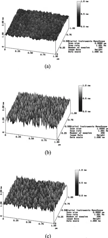
Figure 1a displays the atomic force microscope共AFM兲 surface image of a fresh bare Si wafer. The surface roughness, root mean square共rms兲, is around ⬃0.06 nm. Figure 1b shows the AFM sur-face image of Si wafers after conventional RCA cleaning and wet HF-dipping共Control兲 while Fig. 1c shows the image after the addi-tional new in situ HF vapor cleaning 共HFV兲. The surface of the control sample (rms⬇ 0.15 nm) is rougher than that of the HFV sample (rms⬇ 0.1 nm). This resembles the results reported in Ref. 4, which states that the oxide/Si interface is smoother for the same oxide thickness when grown with in situ native oxide removal.
The poly-Si/Si structures were fabricated to monitor the relative quantity of native oxide for the samples herein. Following conven-zE-mail: [email protected]
Journal of The Electrochemical Society, 149共1兲 G63-G69 共2002兲 0013-4651/2001/149共1兲/G63/7/$7.00 © The Electrochemical Society, Inc.
tional RCA cleaning, the samples were divided into one without a conventional wet HF dip共Native兲, one with a conventional wet HF dip共Control兲, one with an additional in situ HFV, and the poly-Si deposited sequentially without gate oxidation. Figure 2 presents sec-ondary ion mass spectrometry 共SIMS兲 measurements of the depth profiles of interfacial oxygen for the samples. The oxygen peak in-dicates the relative quantity of native oxide. Clearly, wafers pro-cessed through the HF vapor cleaning and poly-Si modules in se-quence without exposure to the ambient have a very low oxygen interface共a native-oxide-free interface兲.
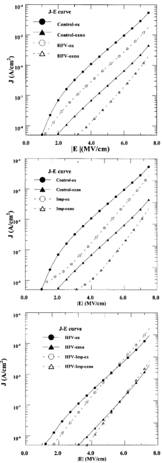
Figure 3a-c shows the leakage current 共J-E兲 characteristics of gate oxides under ⫺Vg injection. HFV treated samples exhibited lower leakage current values than did their counterparts. The exces-sive leakage current in the other samples is attributed to the presence of intrinsic traps that exist before the oxide is stressed. These intrin-sic traps are process-dependent, and thus, are strongly related to the presence of residual native oxide and local thinning in oxide.17,18 After in situ HF vapor cleaning, the native oxide is efficiently re-moved and a uniform gate oxide thickness can be obtained. Further-more, in the low field region, the slope of J-E curve differs signifi-cantly for the control and HFV samples when compared to the dilute dry O2gate oxide, that is, HFV samples exhibit a lower slope than the control sample. Besides, as Fig. 3b and c shows, samples with gate nitrogen implantation exhibit a lower leakage current than do their counterparts. In the low field region, as displayed in Fig. 3c, the slope of the J-E curve is still different for implanted samples and control samples after HFV cleaning. The improvement and the dif-ference of J-E curves are attributed to the incorporation of nitrogen into the gate oxide when nitrogen is implanted in the polysilicon gate.
The subthreshold swing of the HFV-ox共⬃80 mV/decade兲 is bet-ter than that of the control-ox共⬃90 mV/decade兲. Consequently, the interface trap density can be reduced, thus improving the carrier mobility of the deep submicrometer n-MOSFETs by an additional HF vapor cleaning before gate oxidation. Furthermore, the sub-threshold swing of the Imp-ox共⬃74 mV/decade兲 is better than that of the control-ox 共⬃90 mV/decade兲. Meanwhile, the subthreshold swing of the HFV-Imp-ox is also ⬃74 mV/decade. The interface trap density can be reduced and the carrier mobility of deep submi-crometer n-MOSFETs improved by combining in situ HF vapor cleaning and gate nitrogen implantation.
Figure 4a and b illustrates the Qbd characterization of samples under⫺1 mA/cm2injection. The capacitor area is 50⫻ 50 m. The Qbd value is calculated by counting stress time before soft break-down of the gate oxide begins. Qbdis clearly improved by HF vapor cleaning. This improvement is attributed to the removal of native oxide and dramatic reduction of the intrinsic trap17in the gate oxide. Besides, Qbd is also improved by nitrogen implantation. The samples combining HF vapor clean and nitrogen implantation have the best Qbdvalues.
Figure 1.共a兲 The AFM surface image of fresh bare Si wafer. 共b兲 The AFM surface image of Si wafers after conventional RCA clean and wet HF dip 共Control兲 and 共c兲 conventional RCA clean and in situ HFV.
Figure 2. The SIMS depth profile of residual oxygen at the poly-Si/Si
interface.
Journal of The Electrochemical Society, 149共1兲 G63-G69 共2002兲 G64
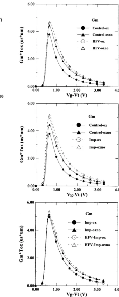
Figure 5a-c presents drain current vs. drain voltage curves of n-MOSFETs with different gate oxide preparations, while Fig. 6a-c depicts the corresponded transconductance characteristics at Vd ⫽ 0.1 V. Notably, both the drain current and transconductance of the HFV samples are higher than those of the control samples. Fur-thermore, the carrier mobility in the channel of MOSFET is well known to be governed by individual contributions from phonons, channel doping impurities, and interface roughness. Coulomb scat-tering is dominated by doping impurities in low-field areas and dominated by interface roughness in high-field areas.4,16,19In a deep submicrometer n-MOSFET, the transverse electric field共that is, the field orthogonal to the gate oxide interface兲 attains values higher than 1 MV/cm, and the energy levels of the channel electrons are strongly quantized even at room temperature, while scattering with surface imperfections degrades electron mobility. Since the typical effective electric field at the threshold is close to or higher than 0.5 MV/cm, the mobility of today’s MOSFET is always surface roughness-limited.19For the control samples, as gate oxide is grown native oxide residues will introduce nonuniform oxide thickness and
Figure 3. The J-E characteristics of gate oxides grown in dilute dry
O2(Tox⫽ 4 nm) and with N2O postoxidation annealing (Tox⫽ 3.9 nm)
under-Vg injection of共a, top兲 control and HF vapor samples, 共b, center兲
control and implanted samples,共c, bottom兲 HF vapor clean and implanted samples.
Figure 4. Qbddistributions of共a, top兲 control and implanted samples 共b,
bottom兲 HF vapor clean and implanted samples under ⫺1 mA/cm2injection.
Figure 5. Drain current curves of共a兲 Control and HF vapor samples, 共b兲
Control and implanted samples,共c兲 HF vapor clean and implanted samples.
Figure 6. The Gmcharacteristics at Vd⫽ 0.1 V of 共a, top兲 Control and HF
vapor samples,共b, center兲 Control and implanted samples, 共c, bottom兲 HF vapor clean and implanted samples.
Journal of The Electrochemical Society, 149共1兲 G63-G69 共2002兲 G66
increase interface roughness, sacrificing the mobility of modern deep submicrometer devices.18Consequently, the drain current and transconductance are both degraded, and thus an additional in situ HF vapor cleaning and transferring of wafers in the closed ambient can reduce native oxide regrowth and possibly enhance surface roughness. This change will significantly improve the performance of the device. Notably, both the drain current and transconductance of the implanted samples are higher than those of the control samples, a feature that is attributed to the incorporation of nitrogen in the implanted samples.7-10
Figure 7 shows the SILC of MOS capacitors under⫺5 mA/cm2 injection共Fowler-Nordheim, F-N, stressing兲. F-N stressing will lead to trap generation, causing reliability problems in the device.20 Ad-ditionally, during F-N stressing, a conductive filament forms locally and is grown in the oxide causing SILC conduction.21,22The SILC is lower for samples with nitrogen implantation. Furthermore, for HF vapor cleaned samples, since the native oxide and the associated intrinsic traps contained in the oxide before stress are efficiently removed smooth interface and uniform oxide can be obtained. The stress induced leakage current of those samples is reduced dramati-cally, and combination of HF vapor cleaning and nitrogen implan-tation significantly reduces the SILC.
Figure 8 illustrates Gmdegradation in 0.35m n-MOSFET de-vices under drain avalanche hot carrier stress at Vds⫽ 3.3 V, Vgs ⫽ 1.15 V. Gmdegradation is significantly improved with the ni-trogen implantation, consistent with previous reports.9,10 Figure 8 also reveals that HF vapor cleaning can improve the hot carrier immunity of n-MOSFET, an improvement that is attributed to the efficient native oxide removal with the subsequent growth of a high quality and reliable ultrathin gate oxide. The combination of HF vapor clean and nitrogen implantation will achieve the best hot car-rier immunity.
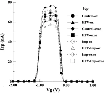
Figure 9 presents the Icp of devices studied herein. The gate length/width of the n-MOSFET used herein was 5/20m, while the measurement frequency was 1 MHz, the amplitude 1.5 V, and source and drain were ground during measurement. The magnitude of the charge pumping current is directly correlated to interface state den-sity (Nit) in the fresh共nonstress devices兲. Meanwhile, the pumping current for the HF vapor cleaned sample is lower than that of the HF dip. Consequently, the interface state density is reduced after HF vapor cleaning, and the interface state density is further reduced by nitrogen implantation. Nitrogen implantation thus suppresses
inter-face generation. This result can be explained by a reduction of highly strained bonds in the oxide films, which can be accomplished owing to the different bonding requirements of segregated nitrogen, as reported by other nitridation techniques.10The existence of native oxide in very thin gate oxide causes integrity degradation because the thickness ratio of the native oxide to net thermal oxide increases as the gate oxide becomes thinner. The thickness of the preoxide in the net thermal oxide must be minimized.23In the case of control-ox, the thickness ratio of native oxide to net thermal oxide signifi-cantly exceeds than that of HFV-ox, as displayed in Fig. 2. This phenomenon degrades the interface of the gate oxide. If nitrogen implantation is applied without the combination of HF vapor clean-ing共Imp-ox兲, the integrity of the gate oxide will still be degraded because of the existence of native oxide in the thin gate oxide. As
Figure 7. The stress induced leakage current 共SILC兲 of MOS capacitors
under⫺5 mA/cm2injection共F-N stressing兲. Figure 8. The G
m degradation in 0.35 m n-MOSFET devices under
channel hot carrier stress; Vds⫽ 3.3 V, Vgs⫽ 1.15 V.
Figure 9. Icpof samples in this experiment.
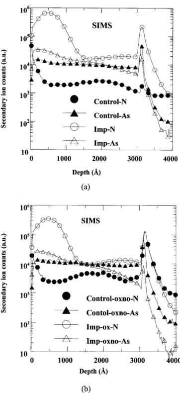
Fig. 9 shows, the pumping current is reduced and reaches its mini-mum after combining nitrogen implantation and HF vapor cleaning. Dopant共As兲 penetration from the polysilicon gate to the sub-strate was also investigated herein. Figure 10a and b shows the SIMS depth profiles of nitrogen and arsenic atoms in the control and implanted samples. The nitrogen atoms were piled up in the poly-silicon bulk and at the gate oxide/poly-silicon substrate interface in im-planted samples. Meanwhile, nitrogen atoms were reported to be able to suppress dopant 共boron兲 penetration from the polysilicon gate to the silicon substrate by the interface and bulk effect.8,12 Interface effects include the modification of dopant segregation into the gate oxide, or a pileup of nitrogen atoms at the poly/oxide
inter-face. An example of a bulk effect is a reduction of dopant共boron兲 diffusivity within the polysilicon bulk.8 Here, nitrogen was im-planted into undoped polysilicon before implantation of the gate electrode dopant 共arsenic, 30 keV, 3 ⫻ 1015 cm⫺2兲. A high tem-perature furnace annealing 共850°C for 30 min兲 was then done to drive the nitrogen共together with the arsenic兲 to the gate oxide in-terface, thus reducing the concentration of nitrogen共and arsenic兲 in the bulk of polysilicon. Figure 10a and b shows that, in the im-planted sample, the arsenic peak nearly coincides with the nitrogen peak in the bulk of polysilicon. Possibly, nitrogen within the poly-silicon bulk is primarily responsible for the suppressing dopant 共ar-senic兲 penetration, thus reducing levels of arsenic released into the gate oxide. Consequently, device performance is improved, as shown in Fig. 5b.
The use of oxynitrides has been proposed as a diffusion barrier to dopant共boron兲 penetration into the channel. However, since nitro-gen incorporation occurs at the bottom gate of the oxide/substrate interface, dopant共boron兲 can still enter and degrade the dielectric at the top polysilicon/gate oxide interface.8 In the case of nitrogen implantation, the nitrogen is introduced into the polysilicon gate and is more effective in suppressing the dopant atom diffusion共herein, arsenic兲 into the gate oxide. This significantly improves the J-E, Id, Gm, Qbd, interface state density, and hot carrier reliability for the oxynitride.
Conclusions
This study demonstrates a high performance and reliable deep submicrometer n-MOSFET with ultrathin gate oxide prepared by combining nitrogen gate electrode implant and native-oxide-free in situ HF vapor preoxidation cleaning. Additional in situ HF vapor cleaning and transferring of wafers in the closed ambient can reduce the regrowth of native oxide and improve the surface roughness. The improved reliability and performance are attributed to the smooth interface and reduced As incorporation in the gate oxide resulting from HF vapor cleaning and nitrogen implantation, respectively. The results presented herein also indicate that the performance and reli-ability, including the leakage current of ultrathin gate oxide, drain current (Id), Gm, charge pumping current (Icp), SILC, Qbd, inter-face state density, and hot carrier reliability of n-MOSFETs are all significantly improved.
Acknowledgments
The authors would like to thank the National Science Council of the Republic of China for financially supporting this research under contract no. NSC89-2215-E009-095.
National Chiao Tung University assisted in meeting the publication costs of this article.
References
1. T. P. Ma, IEEE Trans. Electron Devices, 45, 680共1998兲.
2. C.-M. Yih, S.-M. Cheng, and S. S. Chung, IEEE Trans. Electron Devices, 45, 2343
共1998兲.
3. J. M. Lai, W. H. Chieng, B. C. Lin, A. Chin, and C. Tsai, J. Electrochem. Soc., 146, 2216共1999兲.
4. A. Chin, W. J. Chen, T. Chang, R. H. Kao, B. C. Lin, C. Tsai, and J. C. M. Huang, IEEE Electron Device Lett., 18, 417共1997兲.
5. S. A. Ajuria, B. Maiti, P. J. Tobin, and T. C. Mele, IEEE Electron Device Lett., 17, 282共1996兲.
6. Y. Okada, P. J. Tobin, P. Rushbrook, and W. L. DeHart, IEEE Trans. Electron Devices, 41, 191共1994兲.
7. B. Yu, D.-H. Ju, W.-C. Lee, N. Kelper, T.-J. King, and C.-M. Hu, IEEE Trans. Electron Devices, 45, 1253共1998兲.
8. A. I. Chou, C. Lin, K. Kumar, P. Chowdhury, M. Gardner, M. Gilmer, J. Fulford, and J. C. Lee, in IEEE International Reliability Physics Symposium Proceedings, IRPS, 174共1997兲.
9. T. S. Chao, C. H. Chien, S. K. Chiao, H. C. Lin, M. C. Liaw, L. P. Chen, T. Y. Huang, T. F. Lei, and C. Y. Chang, Digest of Technical Papers of the Symposium on VLSI Technology, 316共1997兲.
10. A. Yasuoka, T. Kuroi, S. Shimizu, M. Shirahata, Y. Okumura, Y. Inoue, M. Inuishi, T. Nishimura, and H. Miyoshi, Jpn. J. Appl. Phys., Part 1, 36, 617共1997兲. 11. T. Kuroi, T. Yamaguchi, M. Shirahata, Y. Okumura, M. Inuishi, and N. Tsubouchi,
Tech. Dig. Int. Electron Devices Meet., 1993, 325. Figure 10. SIMS depth profiles of N and As in control and implanted
samples.
Journal of The Electrochemical Society, 149共1兲 G63-G69 共2002兲 G68
12. J. C. Hu, J. Kuehne, T. Grider, M. Rodder, and I. C. Chen, Digest of Technical Papers of the Symposium on VLSI Technology, 167共1997兲.
13. C. T. Liu, E. J. Lloyd, Y. Ma, M. Du, R. L. Opila, and S. J. Hillenius, Tech. Dig. Int. Electron Devices Meet., 1996, 499.
14. C. T. Liu, Y. Ma, J. Becerro, S. Nakahara, D. J. Eaglesham, and S. J. Hillenius, IEEE Electron Device Lett., 18, 105共1997兲.
15. C. T. Liu, Y. Ma, H. Luftman, and S. J. Hillenius, IEEE Electron Device Lett., 18, 212共1997兲.
16. P. Lange and H. BoneB, M. Hendriks, J. Electrochem. Soc., 146, 2216共1999兲. 17. C. T. Liu, A. Ghetti, Y. Ma, G. Alers, C. P. Chang, K. P. Cheung, J. I. Colonell, W.
Y. C. Lai, C. S. Pai, R. Liu, H. Vaidya, and J. T. Clemens, Tech. Dig. Int. Electron Devices Meet., 1997, 85.
18. H. S. Momose, S.-i. Nakamura, T. Ohguro, T. Yoshitomi, E. Morifuji, T. Morimoto, Y. Katsumata, and H. Iwai, IEEE Trans. Electron Devices, 45, 691共1998兲. 19. G. Mazzoni, A. L. Lacaita, L. M. Perron, and A. Pirovano, IEEE Trans. Electron
Devices, 46, 1423共1999兲.
20. S.-I. Takagi, N. Yasuda, and A. Toriumi, IEEE Trans. Electron Devices, 46, 335
共1999兲.
21. T. P. Chen, S. Li, S. Fung, C. D. Beling, and K. F. Lo, IEEE Trans. Electron Devices, 45, 1972共1998兲.
22. T. P. Chen, S. Li, S. Fung, and K. F. Lo, IEEE Trans. Electron Devices, 45, 1920
共1998兲.
23. K. Makihara, A. Teramoto, K. Nakamura, M. Youn Kwon, M. Morita, and T. Ohmi, Jpn. J. Appl. Phys., Part 1, 32, 1B共1993兲.