第二型能帶結構碲化鋅/硒化錳鋅量子點之光學特性研究
42
0
0
全文
(2) 第二型能帶結構碲化鋅/硒化錳鋅量子點之光學特性研究 Optical characteristics of type-II ZnTe/ZnMnSe quantum dots. 研 究 生:陳筱筑. Student:Hsiao-Chu Chen. 指導教授:周武清教授. Advisor:Prof. Wu-Ching Chou. 國 立 交 通 大 學 電子物理研究所 碩 士 論 文. A Thesis Submitted to Institute of Electrophysics College of Science National Chiao Tung University in partial Fulfillment of the Requirements for the Degree of Master in Electrophysics June 2007 Hsinchu, Taiwan, Republic of China. 中華民國九十六年六月.
(3) 第二型能帶結構碲化鋅/硒化錳鋅量子點之光學特性研究. 研究生:陳筱筑. 指導教授:周武清博士. 國立交通大學電子物理研究所. 中文摘要 本文係利用光激螢光光譜和時間解析光譜量測技術來分析碲化鋅/硒 化錳鋅量子點的光學特性。碲化鋅/硒化錳鋅量子點是以分子束磊晶系統成 長,碲化鋅覆蓋厚度分別為1.8、2.2、2.4、2.7與3.0個原子層。根據反射 式高能電子繞射圖形以及光激螢光譜峰值隨覆蓋層厚度增加而紅移的趨 勢,可以判斷量子點是以Stranski-Kronstonov (S-K) 的模式成長的。隨著雷 射激發的強度增加,我們可以觀測到光激螢光譜峰值能量會有明顯的藍 移,但是,此藍移現象對量子點樣品以及二維結構樣品而言,卻是個別受 到量子點大小分佈以及能帶彎曲效應,不同的兩個物理機制所導致。由時 間解析光譜來分析載子生命期,我們發現載子生命期會隨著碲化鋅覆蓋厚 度的不同而改變,其現象可由能帶彎曲的情形,以及電子電洞波函數的重 疊情形加以說明。進一步量測不同溫度下的時間解析光譜,發現在低溫下 載子會以輻射方式結合,然而當溫度高於50度絕對溫度,載子復合會轉為 非輻射形式。最後,我們發現無外加磁場時,此第二型能帶結構樣品會有 非零圓形極化率產生,主要是因為載子受激發後,受到碲化鋅/硒化錳鋅介 面不均勻電場的影響,進而產生等效內建磁場,造成自旋能帶分裂的現象。. i.
(4) Optical characteristics of type-II ZnTe/ZnMnSe quantum dots. Student:Hsiao-Chu Chen. Advisor:Prof. Wu-Ching Chou. Institute of Electrophysics National Chiao Tung University. Abstract The optical properties of ZnTe/ZnMnSe quantum dots were investigated by photoluminescence (PL) and time-resolved photoluminescence (TRPL) in this thesis. The ZnTe/ZnMnSe quantum dots (QDs) were grown by the molecular beam epitaxy (MBE) and the coverages of ZnTe are 1.8, 2.2, 2.4, 2.7, and 3.0 monolayers (MLs). Stranski-Kronstonov (S-K) growth mode was identified by the reflection high energy electron diffraction patterns and different red-shift slopes with ZnTe coverage for the PL peak energy. In order to verify the type-II band alignment, power-dependent PL was investigated. There is a significant blue-shift of PL peak energy as the excitation power increases. However, the blue-shift of 0D QDs and 2D layer are caused by two different mechanisms. The QD size distribution and band-bending effect result in the blue-shift for 0D QDs and 2D layer, respectively. In order to understand the mechanism of carrier recombination process, the TRPL was also investigated. The coverage dependence of lifetime can be well-explained by band-bending effect and electron-hole wave function overlap. In addition, the temperature-dependent TRPL shows that the carrier ii.
(5) recombination process dominates by radiative channel in low temperature and nonradiative recombination takes over above 50K. Finally, we observed a nonzero circular polarization rate for the type-II structures without external magnetic field. It is attributed to the existence of a built-in magnetic field induced by the motion of carriers under the presence of nonuniform electric field across the interface of ZnTe QDs and ZnMnSe layer. This results in the spin splitting responsible for the nonzero circular polarization rate.. iii.
(6) Acknowledgement 研究所的求學生涯在不知不覺中,即將劃下句點。這兩年在交大的日子,讓我認識 了很多新朋友,不管是學業、研究甚至是待人處世方面,都成長了不少。 這兩年要特別感謝我的指導教授周武清博士,在我從事研究的過程中,提供我足夠 的資源、耐心的教導我、給予我良好的建議,特別是老師協助我解決經濟上的困難,對 我來說這些幫助都是讓我繼續努力下去的動力。還有,要感謝沈志霖教授提供時間解析 光譜量測設備,讓這份論文能有更完整的研究探討;也要感謝實驗室的學長姊們對我的 指導,感謝謝博、楊博、郭博、狗哥、彥丞、京玉、繼組、怡仁、阿邦、龜泰、瑞雯、 阿許、聲嵩、啟仁、維偲、尚樺,教導我實驗上的技術以及分享生活的點滴,特別是謝 博在忙碌中還抽空和我討論,協助我解釋實驗的結果,如果沒有您的幫助,我一定會遇 到更多的挫折;還要感謝實驗室的伙伴阿吉,在最後的關卡一起互相打氣、勉勵,希望 你的努力可以很快看到成果,也祝你減肥成功,恢復帥氣的模樣;還有鏡學、復凱兩位 學弟,希望你們在未來的一年裡,都能順利的完成研究,以及交到女朋友。 另外,我還要感謝我的好友們,皇如、耕宜、子傑、蛋頭、阿杜、美君等等,感謝 你們總是挺我,在我最低潮的時候伸出援手,讓我有勇氣撐過難熬的日子;還有我的男 友明道,謝謝你陪我走過這兩年,照顧我、支持我,是我的精神支柱。 最後,要感謝我的家人,謝謝你們總是忍受我的忙碌,尤其是姊姊,妳總是為我著 想,用最寬容的心體貼我、鼓勵我,因為有妳的加油,才能讓我專心的完成這份論文。. iv.
(7) Index Abstract (Chinese version) ................................................................. i Abstract (English version)................................................................. ii Acknowledgement ............................................................................. iv Index.................................................................................................... v Chapter 1:Introduction................................................................... 1 Chapter 2:Experiment .................................................................... 3 2.1 Sample preparation ............................................................... 3 2.2 Photoluminescence................................................................. 4 2.3 Time-resolved photoluminescence........................................ 4 Chapter 3:Results and Discussion................................................ 12 3.1 Emission properties of ZnTe/ZnMnSe QDs ...................... 12 3.2 Dynamics of carrier recombination.................................... 15 3.3 Polarization at zero magnetic field ..................................... 17 Chapter 4:Conclusions.................................................................. 32 Reference .......................................................................................... 33. v.
(8) Chapter 1:Introduction. The optical properties of excitons confined in semiconductor quantum dots (QDs) have been studied very intensively for recent years. Several QD growth methods have been reported [1-4]. Self-assembled QDs are particularly attractive because of their high structural qualities and excellent optical properties [5-6]. One of the successful applications of self-assembled QD is QD lasers [7]. In addition, the long spin relaxation time, which allows control and manipulation of the electron spin in self-assembled QDs, was discussed [8-9]. The QD systems characterized by the random substitution of a fraction of the original atoms by magnetic atoms are commonly called as diluted magnetic semiconductor QDs (DMS QDs). The DMS QDs have received a great deal of attention because the combination of strong confinement of carriers and sp-d exchange interaction between carriers spin and magnetic ions spin result in special magneto-optical properties. The most common DMS materials are II-Ⅵ compounds (like CdTe, ZnSe, CdSe, etc.), with transition metal ions (like Mn, Fe) substituting their original cations [10-11]. There are also DMS materials based on Ⅳ-Ⅵ [12] and recently Ⅲ-Ⅴ [13] compounds. Most of self-assembled DMS QDs are DMS QDs grown in non-DMS matrix, such as CdMnSe/ZnSe, CdMnTe/ZnTe and so on [14-19]. However, a significant reduction of QD emission efficiency was observed in this system, because there is a relaxation path of carriers into the internal Mn2+ transition [10]. In order to enhance the radiative emission of the QDs, non-DMS QDs embedded in DMS matrix were investigated [20-23]. The samples we studied in this thesis are also non-DMS QDs embedded in DMS matrix. Both types of DMS QDs have potential applications in quantum computation [24] and spin electronic (spintronics) devices [25, 26]. The above mentioned DMS QD systems all have type-I band alignment, which electrons and holes are both confined in QD. In this thesis, we study ZnTe/ZnMnSe DMS QDs with 1.
(9) band alignment of type-II. Holes are confined in the ZnTe QDs, while electrons are localized in ZnMnSe layer. The separation of electrons and holes could result in a longer spin relaxation time [27] than that of type-I QDs. In addition, optical properties of type-II structures are more sensitive to interface electric field caused by carriers accumulation than type-I structures. The special characteristic results in a nonzero circular polarization rate without external magnetic field [28]. In chapter 2, the sample preparations using Veeco Applied EPI 620 MBE system are introduced. In addition, the optical experiment setup, including photoluminescence (PL) and time-resolved PL (TRPL), are presented. In chapter 3, the experimental results about low temperature PL, power-dependent PL, carrier recombination dynamics, and circular polarization PL are discussed. Finally, a brief conclusion is given in chapter 4.. 2.
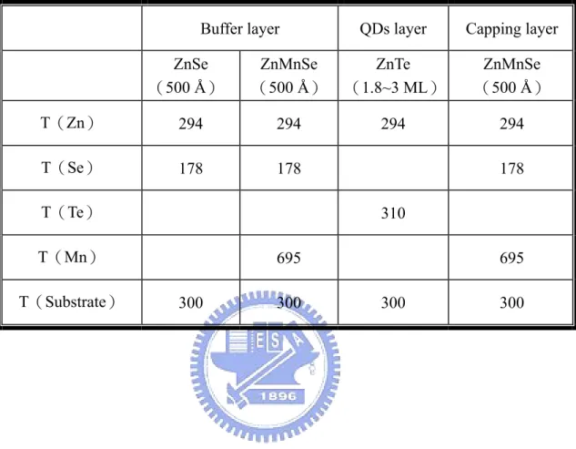
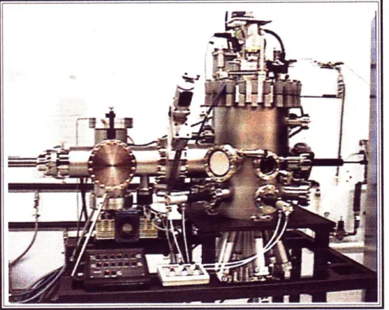
(10) Chapter 2:Experiment. In this chapter, the sample growth of ZnTe/ZnMnSe QDs system and experimental setup used in this thesis were described. The experimental techniques including conventional photoluminescence, polarized photoluminescence and time-resolved photoluminescence are described below.. 2.1 Sample preparation The samples studied in this thesis were grown on GaAs (100) substrates by Veeco Applied EPI620 MBE system shown in Fig. 2-1. The elemental solid source Zn, Mn, Te, and Se were used for the growth of self-assembled ZnTe QDs and ZnMnSe buffers. The growth conditions were listed in Table 2-1. The growth rate for ZnMnSe buffer layer is 0.4 Å/s, whereas the growth rate for the ZnTe QDs is 0.3 Å/s. The effusion cell temperatures of Zn, Mn, Se, and Te are 294, 695, 178, and 310 oC, respectively. Figure 2-2 shows the sample structure of ZnTe/ZnMnSe QDs. Prior to growth procedure, GaAs (100) substrate was etched in a H2O2:NH4OH:H2O (1:5:50) solution for one minute at room temperature, rinsed in flowing de-ionized water about two minutes and dried with high purity-N2. The substrate was adhered to a molybdenum block, and then loaded into a high-vacuum growth chamber. The substrate temperature was then raised to 620~630oC to desorb the oxides. The desorption procedure was monitored by the reflection high energy electron diffraction (RHEED). Then the substrate temperature was decreased to 300 oC for the deposition of ZnSe buffer layer. The ZnSe buffer layer included several MLs grown by migration enhance epitaxy and a thickness of 50 nm grown by conventional epitaxy. Then, a thickness of 50 nm ZnMnSe buffer layer was grown. The average roughness of ZnMnSe buffer layer was approximately 0.5 nm, indicating that the surface of ZnMnSe buffer layer was flat. After the flat ZnMnSe buffer layer was deposited, the growth of the self-assembled 3.
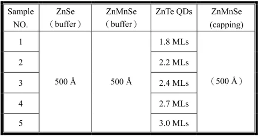
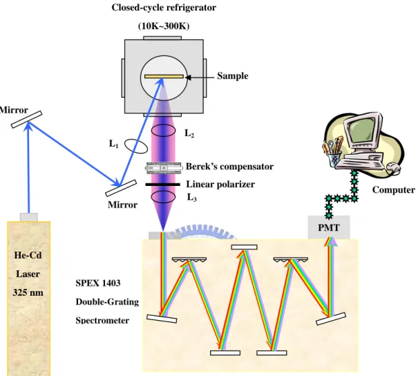
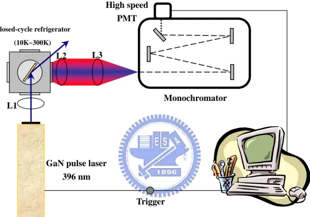
(11) ZnTe QDs started. The growth of ZnTe QDs was turned on for several tens seconds, which corresponds to several mono-layers (MLs). Finally, a ZnMnSe capping layer of about 50 nm was grown to cap the ZnTe dots. The sample list was shown in Table 2-2. The average coverage of ZnTe layers for sample one to five were 1.8, 2.2, 2.4, 2.7 and 3.0 MLs, respectively. The thickness of 1 ML is approximately 0.3 nm.. 2.2 Photoluminescence (PL) The schematic setup of the PL system is shown in Fig. 2-3. The samples were loaded on the cold finger of a closed cycle cryostat. The temperature can be controlled between 10 and 300 K. The 325-nm line of a HeCd laser was used to excite the PL spectra. The incident beam was focused on the sample by a lens (L1). For the polarized PL measurement, a combination of a Berek’s compensator and a linear polarizer was set between lens L2 and L3. The compensator functioned as a quarter wave plate. The linear polarizer can be rotated to measure the right-handed (σ+) or left-handed (σ-) component of the luminescence. Then, lens L3 led the luminescence into the spectrometer. The optical path of circular polarization measurement is carefully confirmed by some standard samples with zero polarization. A SPEX 1403 double-grating spectrometer equipped with a thermoelectrically cooled photo-multiplier tube (R928, Hamamatsu) was used to analyze the PL spectra. The spectrometer was controlled by a computer, which was used to store and plot the collected data.. 2.3 Time-resolved photoluminescence (TRPL) Time-resolved PL was used to study the recombination dynamics of excitons in the ZnTe QDs. The setup of TRPL system was shown in Fig. 2-4. The GaN diode laser (396nm) with a pulse width of 50 ps and a repetition rate of 5 MHz was used as an excitation source. The laser light was focused on the sample by a lens (L1). The combination of lens (L2 and L3) led the luminescence into the spectrometer. The signal was dispersed by a 0.55 m 4.
(12) monochromator and detected by a high-speed photomultiplier tube, followed by a PC plug-in time-correlated counting card. The overall temporal resolution of the time-resolved PL measurement is about 300 ps.. 5.
(13) Table 2-1. Effusion cell temperatures and substrate temperatures for the growth of self-assembled ZnTe/ZnMnSe Quantum Dots. The unit of temperature is ℃. Buffer layer ZnSe (500 Å). QDs layer. Capping layer. ZnMnSe (500 Å). ZnTe (1.8~3 ML). ZnMnSe (500 Å). 294. 294. T(Zn). 294. 294. T(Se). 178. 178. T(Te). 310. T(Mn) T(Substrate). 178. 695 300. 300. 6. 695 300. 300.
(14) Table 2-2. Sample parameters of the ZnTe/ZnMnSe Quantum Dots.. Sample NO.. ZnSe (buffer). ZnMnSe (buffer). ZnTe QDs. 1. 1.8 MLs. 2. 2.2 MLs. 3. 500 Å. 500 Å. 2.4 MLs. 4. 2.7 MLs. 5. 3.0 MLs. 7. ZnMnSe (capping). (500 Å).
(15) Fig. 2-1. Veeco Applied EPI 620 MBE system.. 8.
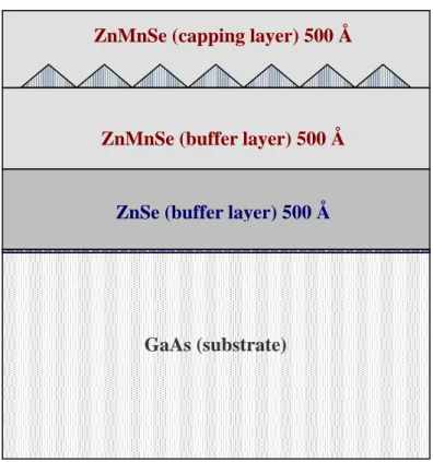
(16) ZnMnSe (capping layer) 500 Å ZnTe QDs layer (1.8~3.0 ML) ZnMnSe (buffer layer) 500 Å. ZnSe (buffer layer) 500 Å. GaAs (substrate). Fig. 2-2. Sample structure of the ZnTe QDs embedded in the ZnMnSe matrix.. 9.
(17) Closed-cycle refrigerator (10K~300K). Sample. Mirror L2 L1 Berek’s compensator. Mirror. Linear polarizer L3. Computer. PMT He-Cd Laser SPEX 1403. 325 nm Double-Grating Spectrometer. Fig. 2-3. Experimental setup for the PL measurements.. 10.
(18) High speed PMT Closed-cycle refrigerator (10K~300K). L2. L3. Monochromator. L1. GaN pulse laser 396 nm Trigger. Fig. 2-4. Experimental setup for the TRPL measurements.. 11.
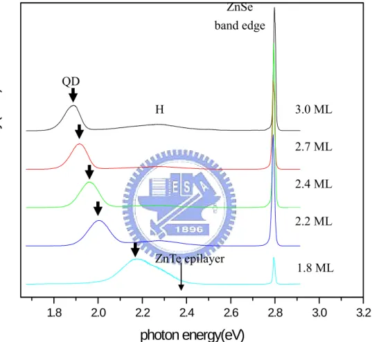
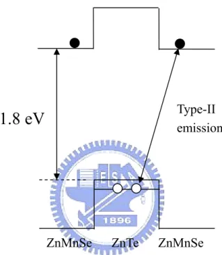
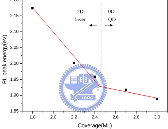
(19) Chapter 3:Results and Discussion. In this chapter, the optical characteristics of ZnTe/ZnMnSe quantum dot (QD) structures were investigated by conventional and time-resolved photoluminescence (PL). Conventional PL was used to detect the ground state transition of the QD samples. To study the type-II band alignments, we also measured the excitation power dependence of spatially indirect transitions in ZnTe/ZnMnSe structures. The difference between two-dimensional (2D) layer structure and zero-dimensional (0D) QD structure is discussed. Time-resolved spectroscopy was used to understand the carrier recombination processes and also verify the dimensional changes of ZnTe/ZnMnSe structures with increasing coverage. Furthermore, circular polarization spectroscopy without an applied magnetic field was utilized to study the spin polarization.. 3.1 Emission properties of ZnTe/ZnMnSe QDs Figure 3-1 shows the PL spectra of ZnTe/ZnMnSe QD structures with different coverage thicknesses of ZnTe layer at low temperature. All of the spectra consist of three emission bands. The sharp emission peak near 2.8 eV is attributed to the near band edge transition of ZnMnSe layer. The other two emission bands observed in the PL spectra from 1.8 to 2.6 eV are associated with the ZnTe layer. The lower-energy emission (labeled by QD in Figure 3-1), which is more sensitive to the change of coverage thickness, is due to the recombination in QD or 2D layer before the QD formation. The peak energies of QD emission bands for 1.8, 2.2, 2.4, 2.7, and 3.0 ML coverage are 2.175, 2.005, 1.963, 1.917, and 1.888eV, respectively. In contrast to type-I semiconductor structures, the energy minima for electrons and holes lie in different layers in type-II structures. In Fig. 3-2, the band alignment of ZnTe/ZnMnSe QD is shown. We assume the band alignment of ZnTe/ZnMnSe QD with low Mn concentration is similar to that of ZnTe/ZnSe QD, which was carefully determined by 12.
(20) the AFM and PL study [29]. This spatially separated electrons and holes will greatly influence optical properties. All of the emission peak energies given above are smaller than that of the band gap energy of ZnTe epilayer. This implies a type-II band alignment for the ZnTe QDs grown in ZnMnSe matrix. The higher-energy PL band (denoted as H in Figure 3-1) near 2.3 eV is much broad and the intensity is smaller than that of the QD PL band. The H emission is ascribed to the emission from the ZnTe/ZnMnSe interface [30]. Figure 3-3 summaries the peak energy shifts of the lower-energy emission for ZnTe/ZnMnSe structures with different coverage thicknesses of ZnTe layer. The red-shift in energy with increasing ZnTe coverage is attributed to the decrease in the quantum confinement of the holes in the ZnTe QDs. Similar to the ZnMnTe /ZnSe QD structure grown in our laboratory [31], the change in red-shift energy can be roughly characterized by two different slopes, as observed in the Figure 3-3. The peak energy decreases promptly with increasing ZnTe coverage when the ZnTe coverage is less than 2.4 ML. However, when the coverage exceeds 2.7 ML, the decrease of peak energy becomes smooth. The critical thickness of the two slopes is between 2.4 and 2.7 ML. For the ZnTe coverage with thickness thinner than the critical thickness, the PL emission origins from the transitions in 2D layer, while 0D QD emission is expected for samples with thicker ZnTe coverage thickness. This result was also confirmed by the study of RHEED patterns. Figure 3-4(a), (b), and (c) show the RHEED patterns of samples with 1.8, 2.4, and 2.7 ML ZnTe coverage, respectively. The streaky RHEED pattern of 1.8 ML results from the two-dimensional layer. As the ZnTe coverage increases to 2.4 ML, the RHEED pattern starts to transfer from streaky to spotty. This indicates a growth transition from a two-dimensional layer growth to a three-dimensional island growth and implies the formation of the ZnTe QDs at ZnTe coverage thickness above 2.4 ML. The excitation power dependence of spatially indirect transitions of ZnTe 2D layer and 0D quantum dot were investigated. In Fig. 3-5, we show the relation between the PL peak 13.
(21) energy and the excitation power of three samples with coverage of 2.2 ML, 2.4 ML and 2.7 ML. When the excitation power was increased, blue-shifts for three samples were observed. The lines fit the blue-shifts of three samples using the power function described by Y=a+bxs. The powers (s) for samples of coverage with 2.2 ML, 2.4ML, and 2.7 ML are 0.32 (dashed line), 0.3 (dot line), and 0.1(solid line), respectively. The cubic root (s=0.33) power dependence of PL peak shift caused by the band-bending effect is characteristic of type-II quantum wells and has been reported theoretically [32, 33]. The band-bending effect is caused by the spatial separation of holes confined in the ZnTe layer and the hole-attracted electrons localized in the nearby ZnMnSe regions. With the increasing excitation power, the strong band-bending effect (red-shift) accompanying with the carrier filling effect (blue-shift) results in a theoretical-predicted blue-shift of PL peak with the 1/3 of the excitation power [32, 33]. It corroborates the previous result that the 2.2 ML and 2.4 ML samples are 2D layer structures. However, in the case of 2.7 ML QD structure, only a few holes are allowed to be confined in each QD. As a result, the band-bending effect does not play important role and the blue-shift of PL peak deviates from the cubic root. The carrier distribution effect is a possible mechanism responsible for the blue-shift of 0D QD sample. At the beginning, the carriers are excited to the barrier by the He-Cd laser of the wavelength with 325 nm and then quickly transfer to the QD. The transfer behavior is a selection effect which decides the carriers to transfer to the lower energy states (larger QDs) first. As the excitation power increases, the carriers will gradually fill in the smaller QDs. This will result in a blue-shift with increasing power intensity. Fig. 3-6(a) shows a simple schematic diagram for the carrier filling distribution of different QD sizes as excitation power increases. The estimated power-dependent blue-shift is shown in Fig. 3-6(b). The power of the estimated blue-shift for QD size filling effect is about 0.11 and is close to the experimental result of QD sample with coverage of 2.7 ML. It indicates the excitation power-dependent PL is greatly affected by the QD size distribution. 14.
(22) 3.2 Dynamics of carrier recombination In order to understand the mechanism of carrier recombination process for this type-II QD system, the TRPL was investigated. The experimental PL decay profiles (open circle) measured for the ZnTe QDs sample with 2.4 ML coverage is shown in Fig. 3-7. The decay time is composed of a faster initial component and a slower tail component. In order to resolve the time constants, all of the experimental data were fitted with two-exponential function described by I (t ) = I1 exp(−t / τ 1 ) + I 2 exp(−t / τ 2 ). (3-1). Where I(t) is the PL intensity at time t, I1 and I 2 are the relative intensity for τ 1 and τ 2 , respectively. τ 1 and τ 2 are lifetimes of two different recombination mechanism. The fit for the experimental data is shown by the solid line. The time constants τ 1 and τ 2 are 3.2 ns and 74.7 ns, respectively. The lifetime of carrier recombination is inverse proportion to the wavefunction overlap of electrons and holes [34]. The observed two-exponential decay can be explained by the spatial separation of charges. After the photoexcitation, a dipole layer is formed between the holes in the ZnTe layer and the electrons attracted from the surrounding ZnMnSe regions. This field-induced band-bending effect makes the electron wavefunction closer to the ZnTe region. The initial faster time constant is attributed to the increasing spatial overlap due to the band-bending effect. When the majority of the carriers have recombined, the wavefunction overlap decreases and the band-bending effect is negligible. This will lead to a slow radiative recombination process and results in a longer decay time. Therefore, the slow decay time is attributed to the decay time of the ground state exciton. Because of the nature of type-II QDs structure of ZnTe/ZnMnSe, holes are confined in the ZnTe layer and electrons are localized in ZnMnSe layer around the dots. Due to the less electron-hole overlap in type-II band structure, the measured lifetimes are much longer than the radiative lifetime of type-I QDs [35-37].. 15.
(23) In Fig. 3-8 we show coverage thickness dependence of the exciton decay times. The exciton decay time increases with increasing coverage and starts to decrease above 2.7 ML. We explain the result by separating the data into two regions: 2D layer and 0D QD. In the 2D layer case, the lifetime increases with the coverage thickness due to the increasing electron and hole separation. However, in the QD case, the recombination coefficient depends crucially on the portion of hole wavefunction confined in QD structure. Figure 3-9 shows the schematic representations for the wavefuntion distribution for different case. For the 2D layer case, the wavefunction of holes is located at the center of 2D layer. When the coverage thickness increases, the portion of hole wavefunction decreases at the edge and causes a less electron-hole wavefunction overlapping shown in Fig. 3-9 (a) to (b). Thus, the decay time of the ground state transition becomes longer with increasing coverage. On the contrary, the wavefunction of holes starts to move in quantum dot as the dot formed as shown in Fig. 3-9 (c). Increasing dot size makes the ground state energy become lower and leads the wavefunction of holes closer to ZnMnSe capping layer shown in Fig. 3-9 (d). Hence, the overlap of electron-hole wavefunction enhances and results in a shorter decay time. Figure 3-10 shows the spectral distribution of decay time of ZnTe/ZnMnSe QDs with coverage thickness of 2.7 ML. As shown in the figure, the exciton decay time depends on the monitored emission energy and is shorter for higher energies. Carriers in the small QDs, whose ground state energy is larger, can transfer to the lower energy state in the adjacent larger QDs [37]. The extra transfer channels will result in a faster decay rate for higher-energy transition. The PL in the lower-energy transition has a longer decay time due to the increase in the number of carriers that relaxed from the smaller QDs. We also examined the temperature effect on the indirect type-II transition in ZnTe/ZnMnSe QD structures. Figure 3-11 shows the temperature dependence of lifetime at peak energy with 2.7 ML coverage. The ground state exciton decay time is almost constant with temperature below 50 K. This is not surprising because the thermal distribution of radiative rate was greatly suppressed in QD structures. The 16.
(24) exciton decay time, however, decreases quickly with increasing temperature above 50 K. It is because nonradiative recombination dominates the transition above 50K.. 3.3 Polarization of zero magnetic field In order to study the spin polarization degree without an applied magnetic field (B), the circular polarization PL was investigated. Figure 3-12 shows the PL spectra with σ + (dash line) and σ − (solid line) circular polarization for the 2.7 ML ZnTe/ZnMnSe QDs without external magnetic field. We can clearly see that the polarization rate ( P ) is nonzero, where P is defined as. P=. Iσ + − Iσ −. (3-2). Iσ + + Iσ −. In this expression, I σ + ( I σ − ) is the integrated PL intensity of σ + ( σ − ) polarization. The calculated value of P is about -7 % in this sample. It’s quite a special phenomenon because the spin orientation of carriers should be randomized before recombination for B=0 [38]. This result implies that some built-in B exists in the type-II structures. The Mn spin alignment is not essential for the built-in B. The results show that the nonzero polarization is less sensitive to thermal energy at least for temperature below 100 K. However, the spin polarization induced by Mn should be greatly suppressed with increasing temperature [39]. We believe that this phenomenon is similar to those found in type-II semiconductor heterostructures [40], where a nonzero spin splitting is possible with a built-in B induced by the motion of carriers under the presence of nonuniform electric field across the interfaces of ZnTe QDs and ZnMnSe layer. The nonuniform strain induced internal magnetic field might be in the minus z-direction because the negative polarization rate changes to positive by an external magnetic field applied to z-direction [30]. The schematic diagram was shown in Fig. 3-13. Because of the built-in magnetic field, the carriers of higher-energy spin state will easily flip to the lower-energy spin state and result in a negative polarization rate as shown in Fig. 3-13(b). 17.
(25) This investigation shows that the carrier recombination process of type-II structures dominated by the interface electric field enormously. It also provides a possibility to manipulate the spin degree by tuning the internal strain for zero applied magnetic field.. 18.
(26) PL Intensity(a.u.). ZnSe band edge. QD 3.0 ML. H. 2.7 ML 2.4 ML 2.2 ML ZnTe epilayer. 1.8. 2.0. 2.2. 2.4. 2.6. 1.8 ML. 2.8. 3.0. 3.2. photon energy(eV) Fig. 3-1. Low temperature PL spectra of ZnTe/ZnMnSe QDs for ZnTe coverages of 3.0, 2.7, 2.4, 2.2, and 1.8 MLs.. 19.
(27) Type-II emission. 1.8 eV. ZnMnSe. ZnTe. ZnMnSe. Fig. 3-2. Schematic diagram of type II band alignment for ZnTe/ZnMnSe QDs.. 20.
(28) 2.20. 2D layer. 2.15. 0D QD. PL peak energy(eV). 2.10. 2.05. 2.00. 1.95. 1.90. 1.85 1.8. 2.0. 2.2. 2.4. 2.6. 2.8. Coverage(ML) Fig. 3-3. Peak energy versus ZnTe coverage.. 21. 3.0.
(29) (a) 1.8 ML. (b) 2.4 ML. (c) 2.7 ML. Fig. 3-4. RHEED pattern of ZnTe QDs with different coverage.. 22.
(30) 2.2 ML 2.4 ML 2.7 ML s=0.30 s=0.32 s=0.10. PL peak energy shift(eV). 0.04. 0.03. 0.02. 0.01. 0.00 0. 2. 4. 6. 8. 10. 12. Power(mW). Fig. 3-5. Excitation power dependence of PL peak energy shifts for samples with coverage of 2.2 ML ,2.4 ML and 2.7 ML.. 23.
(31) dot size distribution carrier filling distribution. Intensity. 140000. 70000. Power. 0 1.8. 2.1. size distribution. estimated data 1.91. Peak energy (eV). 1.90. S=0.11 1.89. 1.88. 1.87. 1.86 0. 2. 4. 6. 8. 10. Power (mW). Fig. 3-7. (a) Schematic diagram of the excitation power dependence of the carrier filling distribution for different QD sizes. (b) The estimated peak energy blue-shifts.. 24.
(32) τ 1 = 3.2(ns). fast ( τ 1 ). PL Intensity(a.u.). τ 2 = 74.7(ns). slow ( τ 2 ). 0. 50. 100. 150. Time(ns). Fig. 3-7. TRPL of ZnTe QDs sample with 2.4 ML monitored at peak energy (1.93 eV). The solid line is fitted by a two-exponential decay function.. 25.
(33) 90. ground state exciton decay time. Decay time(ns). 80. 70. 60. 50. 2-D layer. 0-D QD. 40. 1.8. 2.0. 2.2. 2.4. 2.6. 2.8. 3.0. Coverage(ML). Fig. 3-8. ZnTe coverage dependence of the ground state exciton decay time.. 26.
(34) ZnMnSe. ZnTe ZnMnSe. ZnMnSe. (a) ZnMnSe. ZnTe. ZnMnSe. ZnMnSe. (c). ZnTe. (b) ZnTe. ZnMnSe. ZnMnSe. (d). Fig. 3-9. Schematic representations for the wavefuntion distribution of electron (light shadow) and hole (dark shadow) for (a) thin 2D layer, (b) thicker 2D layer, (c) small 0D QD, and (d) larger 0D QD without considering wetting layer.. 27.
(35) ground state exciton decay time PL. 90. PL Intensity(a.u.). Decay time(ns). 80. 70. 60. 50. 40 1.8. 2.0. Photon energy(eV) Fig. 3-10. Broad band time-resolved PL of ZnTe QDs with 2.7 ML coverage.. 28.
(36) 80. ZnTe/ZnMnSe 2.7 ML ground state decay time. 75. Exciton decay time(ns). 70 65 60 55 50 45 40 0. 20. 40. 60. 80. 100. 120. 140. Temperature(K). Fig. 3-11. Temperature-dependent lifetime at peak energy for QD of 2.7 ML coverage.. 29.
(37) 20000. σσ+. PL Intensity(a.u.). polarization~-7%. 10000. 0. 1.65. 1.70. 1.75. 1.80. 1.85. 1.90. 1.95. 2.00. 2.05. 2.10. photon energy(eV). Fig. 3-12. PL spectra with σ + (dash line) and σ − (solid line) circular polarization for the 2.7 ML ZnTe QDs at external magnetic field B=0.. 30.
(38) ZnMnSe (capping layer) 500 Å ZnTe QDs layer (1.8~3.0 ML) ZnMnSe (buffer layer) 500 Å. Bin ZnSe (buffer layer) 500 Å. Bex. GaAs (substrate). -1/2. +1/2 σ-. σ+. +3/2. -3/2. Fig. 3-13. The schematic diagram of built-in magnetic field in the ZnTe /ZnMnSe structure (a) and spin relaxation process (b).. 31.
(39) Chapter 4:Conclusions. The optical properties of type-II DMS ZnTe/ZnMnSe QDs grown by the molecular beam epitaxy were investigated by conventional PL and TRPL in this study. The type-II emission peak energies of samples with 1.8, 2.2, 2.4, 2.7, and 3.0 ML coverage are 2.175, 2.005, 1.963, 1.917, and 1.888 eV, respectively. S-K growth mode was identified by the RHEED patterns and different red-shift slopes of the PL peak energy with increasing ZnTe coverages. The excitation power dependence of spatially indirect transitions of ZnTe/ZnMnSe QDs shows a significant blue-shift for PL peak energy. The blue-shift of 0D QDs and 2D layer are caused by two different mechanisms. The QD size distribution and band-bending effect result in the blue-shift for 0D QDs and 2D layer, respectively. In addition, the radiative decay time is composed of a faster initial component and a slower tail component. The initial faster time constant is attributed to the increasing spatial overlap due to the band-bending effect and slower decay time is attributed to the recombination time of ground state transition. The exciton decay time of samples with different coverages is well-explained by wave function overlap. In addition, the temperature dependent time-resolved PL shows that the carrier recombination process dominated by radiative channel in low temperature but by nonradiative channel above 50K. Finally, a non-zero circular polarization of PL at the absence of magnetic field is attributed to the accumulation of interface charges confined in adjacent layers. This type-II QD system could be a potential candidate for the spintronics devices.. 32.
(40) Reference [1] L. V. Titova, J. K. Furdyna, M. Dobrowolska, S. Lee, T. Topuria, P. Moeck, and N. D. Browning, Appl. Phys. Lett. 80, 1237 (2002). [2] L. Landin, M.S. Miller, M.E. Pistol, C.E. Pryor, L. Samuelson, Science 280, 262 (1998). [3] G. Bacher, T. Kummell, D. Eisert, A. Forchel, B. Konig, W. Ossau, C. R.Becker, and G. Landwehr, Appl. Phys. Lett. 75, 956 (1999) [4] D. J. Norris, N. Yao, F. T. Charnock, and T. A. Kennedy, Nano. Lett. 1, 3 (2001). [5] P. R. Kratzert, J. Puls, M. Rabe, and F. Henneberger, Appl. Phys. Lett. 79, 2814 (2001). [6] S.H. Xin, P.D. Wang, Aie Yin, C. Kim, M. Dobrowolska, J.L. Merz, J.K. Furdyna, Appl. Phys. Lett. 69, 3884 (1996). [7] S. Makino, T. Miyamoto, T. Kageyama, N. Nishiyama, F. Koyama, K. Iga, J. Cryst. Growth 221, 561 (2000). [8] D. Gammon, E. S. Snow, B. V. Shanabrook, D. S. Katzer, and D. Park, Science 273, 87 (1996). [9] S. Mackowski, T. A. Nguyen, H. E. Jackson, and L. M. Smith, Appl. Phys. Lett. 83, 5524 (2003) [10] C. S. Kim, M. Kim, S. Lee, J. Kossut, J. K. Furdyna, and M. Dobrowolska, J. Cryst. Growth 214, 395 (2000). [11] P. R. Kratzert, J. Puls, M. Rabe, and F. Hennenberger, Appl. Phys. Lett. 79, 2814 (2002). [12] Heremans, J. and Partin, D. L., Phys. Rev. B 37, 6311 (1988). [13] H. Ohno, A. Shen, H. Munekata et al., Appl. Phys. Lett., 69, 363 (1996). [14] S. Mackowski, S. Lee, J. K. Furdyna, M. Dobrowolska, G. Prechtl, W. Heiss, J. Kossut and G. Karczewski, Phys. Stat. Sol. (b) 229, 469 (2002). [15] A. V. Chernenko, P. S. Dorozhkin, V. D. Kulakovskii and A. S. Brichkin, Phys. Rev. B 33.
(41) 72, 045302 (2005). [16] T. Gurung, S. Mackowski, H. E. Jackson, L. M. Smith, W. Heiss, J. Kossut and G. Karczewski, J. Appl. Phys. 96, 7407 (2004) [17] Y. Terai, S. Kuroda, and K. Takita, Appl. Phys. Lett. 76, 2400 (2000). [18] S. Mackowski, H. E. Jackson, L. M. Smith, J. Kossut, G. Karczewski and W. Heiss, Appl. Phys. Lett. 83, 3575 (2003). [19] G. Prechtl, W. Heiss, S. Mackowski, and E. Janik, Appl. Phys. Lett. 78, 2140 (2001). [20] J. Seufert, G. Bacher, M. Scheibner, A. Forchel, S. Lee, M. Dobrowolska and J. K.Furdyna, Phys. Rev. Lett. 88, 027402 (2002). [21] E. Oh, K. J. Yee, S. M. Soh, J. U. Lee, J. C. Woo, H. S. Jeon, D. S. Kim, S. Lee, J. K. Furdyna, H. C. Ri, H. S. Chany and S. H. Park, Appl. Phys. Lett. 83, 4604 (2003). [22] G. Bacher, H. Schomig, M. K. Welsch, S. Zaitsev, V. D. Kulakovskii, A. Forchel, S. Lee, M. Dobrowolska, J. K. Furdyna, B. Konig and W. Ossau, Appl. Phys. Lett. 79, 524 (2001). [23] K. Shibata, K. Takabayashi, I. Souma, J. Shen, K. Yanata, and Y. Oka, Physica E (Amsterdam) 10, 358 (2001). [24] D. Loss, and D. P. DiVincenzo, Phys. Rev. A 57, 120 (1998). [25] P. Recher, E. V. Sukhorukov, and D. Loss, Phys. Rev. Lett. 85, 1962 (2000). [26] K. Chang, K. S. Chan, and F. M. Peeters, Phys. Rev. B 71, 155309 (2005). [27] A. Murayama, T. Asahina, K. Nishibayashi, I. Souma, and Y. Oka, J. Appl. Phys. 100, 084327 (2006). [28] M. C. Kuo, J. S. Hsu, J. L. Shen, K.C. Chiu, W. C. Fan, Y. C. Lin, C. H. Chia, W. C. Chou, M. Yasar, R. Mallory, A. Petrou, and H. Luo, Appl. Phys. Lett. 89, 263111 (2006). [29] C. S. Yang, Y. J. Lai, W. C. Chou, W. K. Chen, M. C. Lee, M. C. Kuo, J. Lee, J. L. Shen, D. J. Jang, and Y. C. Cheng, J. Appl. Phys. 97, 033514 (2005). 34.
(42) [30] C. S. Yang, D. H. Hong, C. Y. Lin, W. C. Chou, C. S. Ro, W. Y. Uen, W. H. Lan, and S. L. Tu, J. Appl. Phys. 83, 2555 (1998). [31] 郭明錦,「第二型能帶結構碲化錳鋅稀磁性半導體量子點」,私立中原大學,博士 論文,民國95年。 [32] C. M. Lin, Y. F. Chen, Appl. Phys. Lett. 85, 2544 (2004). [33] N. N. Ledentsov, J. Bohrer, M. Beer, F. Heinrichsdorff, M. Grundmann, D. Bimberg, S. V. Ivanov, B. Ya Meltser, S. V. Shaposhnikov, I. N. Yassievich, N. N. Falev, P. S. Kopev, and Zh. I. Alferov, Phys. Rev. B 52, 14058 (1995). [34] H. Born, L. Muller-Kirsch, R. Heitz, phys. stat. sol. (b) 228, No.3, R4-R5(2001) [35] T. Y. Lin, D. Y. Lyu, J. Chang, J. L. Shen, and W. C. Chou, Appl. Phys. Lett. 88, 121917 (2006). [36] C. K. Sun, G. Wang, J. E. Browers, B. Brar, H. R. Blank, H. Kroemer, and M. H. Pilkuhn, Appl. Phys. Lett. 68, 1543 (1996). [37] M.E. Lee, Y.H. Chung, C.S. Yang, W.C. Chou, Y.C. Yeh, C.L. Wu, and D.J. Jang, Physica E 26, 422 (2005). [38] S. Lee, M. Dobrowolska, J. K. Furdyna, Phys. Rev. B 72, 075320 (2005). [39] S. Mackowski, T. Gurung, T. A. Nguyen, H. E. Jackson, L. M. Smith, G. Karczewski and J. Kossut, Appl. Phys. Lett. 84, 3337 (2004). [40] G. Lommer, F. Malcher, and U. Rössler, Phys. Rev. Lett. 60, 728 (1988).. 35.
(43)
數據
+7

相關文件
The Secondary Education Curriculum Guide (SECG) is prepared by the Curriculum Development Council (CDC) to advise secondary schools on how to sustain the Learning to
Students are asked to collect information (including materials from books, pamphlet from Environmental Protection Department...etc.) of the possible effects of pollution on our
Wang, Solving pseudomonotone variational inequalities and pseudocon- vex optimization problems using the projection neural network, IEEE Transactions on Neural Networks 17
Hope theory: A member of the positive psychology family. Lopez (Eds.), Handbook of positive
volume suppressed mass: (TeV) 2 /M P ∼ 10 −4 eV → mm range can be experimentally tested for any number of extra dimensions - Light U(1) gauge bosons: no derivative couplings. =>
Define instead the imaginary.. potential, magnetic field, lattice…) Dirac-BdG Hamiltonian:. with small, and matrix
The existence of cosmic-ray particles having such a great energy is of importance to astrophys- ics because such particles (believed to be atomic nuclei) have very great
incapable to extract any quantities from QCD, nor to tackle the most interesting physics, namely, the spontaneously chiral symmetry breaking and the color confinement..
