國立交通大學
顯示科技研究所
碩士論文
紫外光於 PMMA 有機薄膜電晶體
之光響應提升研究
UV-enhanced Photo responsivity on
PMMA-OTFTs
研究生:顏睿志
指導教授:冉曉雯 博士
紫外光於 PMMA 有機薄膜電晶體之光響應提升研究
UV-enhanced Photo responsivity on PMMA-OTFTs
研 究 生:顏睿志 Student:Ruei-Chih Yan
指導教授:冉曉雯 博士 Advisor:Dr. Hsiao-Wen Zan
國 立 交 通 大 學
光電工程學系 顯示科技研究所
碩 士 論 文
A Thesis
Submitted to Department of Photonics Display Institute
College of Electrical Engineering and Computer Science National Chiao Tung University
in partial Fulfillment of the Requirements for the Degree of
Master in
Electro-Optical Engineering June 2007
Hsinchu, Taiwan, Republic of China
紫外光於 PMMA 有機薄膜電晶體之光響應提升研究
研究生:顏睿志 指導教授:冉曉雯 博士
國立交通大學
顯示科技研究所碩士班
摘要
在本研究中,以加熱固化的方式,將可溶性的甲基丙烯酸甲酯製作成有機 薄膜電晶體的閘極介電層。並利用紫外光,對甲基丙烯酸甲酯-閘極介電層進行 改質。根據觀察,經過紫外光改質後的閘極介電層,有機薄膜電晶體的臨界電壓 將會降低、次臨界幅擺增加、而載子的場效飄移率則沒有顯著的變化。在光照射 有機薄膜電晶體的實驗中,以波長為 460 奈米的光線對元件進行照射。經過紫外 光改質後的元件,光照射時會觀察到一個較大的臨界電壓飄移與光響應。若對元 光照特性進行時間相依的分析,則發現紫外光改質後的元件有較短的飽和時間與 較長的回復時間。為找出紫外光改質影響元件特性差異的原由,我們藉著材料分 析與介電層的漏電分析,各自排除紫外光改質後影響有機半導體膜內部結構與介 電層內產生捕捉缺陷,而主導特性差異的可能性。最後,我們推測元件電特性的 差異可能是來自於半導體與介電層間、因紫外光改質而產生介面的捕捉缺陷態所 主導。並以一系列的時間常數特性來加以驗證提出的假設。UV-enhanced Photo responsivity on PMMA-OTFTs
Student:Ruei-Chih Yan Advisor:Dr. Hsiao-Wen Zan
Display Institude
National Chiao Tung University
Abstract
In this study, with the thermal solidification method, the soluble
Polymethylmethacrylate (PMMA) was used as the gat-dielectric of organic thin film
transistors (OTFTs). Furthermore, we treated the PMMA gate-dielectric with the
UV-light treatment. According to our observation, the OTFTs with UV-light
treatment on gate-dielectric, the threshold voltage will be reduced, the subthreshold
swing will be increased, however, no significant change in field-effect mobility was
observed. In the OTFT experiments under light-irradiation, the devices was
irradiated with a ray at a wavelength about 460nm. Among the OTFTs with
UV-light treatment on gate-dielectric, when the light-irradiation was turn on, a larger
threshold voltage shift and phonic responsivity will be found. If we further analyzed
the time-dependent OTFT characteristics after the light-irradiation, the OTFTs with
In order to find out the origin of UV-light treatment on OTFT property variation, we
tried to introduce the material analysis and dielectric-leakage analysis to rule out the
effects of UV-light treatment on organic semiconductor inertial structure and the traps
inside the dielectric film, respectively. Finally, we presumed the OTFT property
variation should be dominated by the interface traps between the organic
semiconductor film and the dielectric film, which may be created by the UV-light
treatment. The proposed assumption is also verified by a serious time-constant
誌謝
兩年時間的飛逝,回首兩年前,懷抱著期望與夢想進入交大。在求學過程中, 遇到了許多困難與考驗,這些考驗使自己在思想或能力上都成長許多。首先要感 謝我的指導教授冉曉雯老師,感謝冉老師帶領我進入 OTFT 的領域,使我有機會 在這塊領域著墨,並從研究當中讓我了解到一個研究者該有的執著與專業。 感謝實驗室的博班學長:國錫學長、政偉學長、士欽學長,在這兩年來的幫 助與鼓勵。尤其是國錫學長,在我這兩年來的研究生涯裡,用心的教導我實驗方 法提供實驗上的想法,並在心情低落時給予我適時的開導,且不辭辛勞地協助我 完成我的碩士論文。也要感謝實驗室的同學:光明、而康、德倫以及同為 OTFT 組的皇維、廷遠、芸嘉、文馨,這兩年來的互相打氣,互相砥礪,一起努力堅持 到最後。有你們的陪伴,讓我在這兩年研究生涯中更為甘甜回味。 最後感謝我的父母,感謝你們一路的陪伴與支持,沒有你們,就不會有今日 的我。Contents
Abstract (Chinese)
Ι
Abstract (English)
II
Acknowledgement
IV
Contents
V
Table Captions
VII
Figure Captions
VIII
Chapter 1. Introduction
1-1 Introduction of Organic Thin Film Transistors (OTFTs) 1 1-2 Spin-on Coated Dielectrics 2 1-3 Application of Organic Transistors to Optical Devices 3
1-4 Motivation 3
1-5 Thesis Organization 4
Chapter 2. Theoretical Background of OTFTs
2-1 Introduction 5 2-2 Transportation Mechanisms of Organic Semiconductor 5 2-3 Photonic excitation on Organic Devices 8 2-4 Parameter Extraction 11 2-4-1 Mobility 11 2-4-2 Threshold voltage 12 2-4-3 Subthreshod swing 12 2-4-4 Responsivity 13
Chapter 3. Experiments
3-1 PMMA Dielectric Fabrication and UV-light Treatment 14 3-2 PMMA-OTFTs Fabrication 14 3-3 Photonic excitation 16
Chapter 4. Result and Discussion
4-1 Electrical Properties of PMMA Dielectric 17 4-1-1 Fabrication of PMMA dielectrics and relative dielectric properties 17 4-1-2 UV treatment on PMMA dielectric 18
4-2 Characteristics of OTFTs with distinct PMMA-dielectrics 19
4-3 Characteristics of light-illumination on PMMA-OTFTs 20
4-4 Time-dependent parameter analysis under and after light-illumination 21
4-5 Material analysis on PMMA-OTFTs 23
4-6 Plansible origin of the enhancement on photo responsivity 25
Chapter 5. Conclusion
5-1 Conclusion 28References
30Tables
34Figures
37Profile
56Table Captions
Table I The comparison of the different polymer OTFTs electrical properties. Table II The comparison of untreated and UV-treated PMMA dielectrics properties. Table III Time dependent analysis on PMMA-OTFT parameter
Figure Captions
Chapter 3
Fig. 3-1 The cross-section of PMMA-OTFT device. Fig. 3-2 The optical image of PMMA-OTFT.
Fig. 3-3 The experimental diagram of probing stage with a light source.
Chapter 4
Fig. 4-1 The SEM images of PMMA films rotated at 2000 to 6000 RPM are shown in Fig. (a), Fig. (b), and Fig. (c), respectively. The thickness values are about 450, 300, 200 nm, respectively.
Fig. 4-2 The capacitance of the Au/PMMA/Pd/Ni MIM structure as a function of the gate voltage at different rotated speed.
Fig. 4-3 The leakage current of the Au/PMMA/Pd/Ni MIM structure as a function of the electric field at different rotated speed.
Fig. 4-4 The summary of the capacitance and leakage current at different rotated speed are shown in Fig. (a) and Fig. (b).
Fig. 4-5 The atomic force microscope (AFM) image of untreated and UV-treated PMMA dielectric film are shown in Fig. (a) and Fig.(b).
Fig. 4-6 The transfer characteristics of OTFT with untreated PMMA dielectric and UV-treated dielectric are shown in Fig. (a) and Fig. (b).
Fig. 4-7 The transfer characteristics and the plot of square root of drain current versus the gate voltage with untreated PMMA dielectric under light-illumination and light-off are shown in Fig. (a) and Fig. (b).
Fig. 4-8 The transfer characteristics and the plot of square root of drain current versus the gate voltage with UV-treated PMMA dielectric under light-illumination and light-off are shown in Fig. (a) and Fig. (b).
Fig. 4-9 Photo responsivity is plotted as a function of gate-voltage of the untreated and UV-treated OTFT (illumination time is 40s~1000s) are shown in Fig. (a) and Fig. (b).
Fig. 4-10 The experimental data and the fitting-curves of threshold voltage shift is plotted as a function of time, when the PMMA-OTFTs are illuminated with light and the light-illumination is turn off are shown in Fig. (a) and Fig. (b).
Fig. 4-11 The X-ray diffraction (XRD) curves of pentacene film on untreated PMMA dielectric and UV-treated PMMA dielectric are shown in Fig. (a) and Fig. (b).
Fig. 4-12 The Raman spectrum of pentacene film on untreated PMMA dielectric and UV-treated PMMA dielectric are shown in Fig. (a), Fig. (b), Fig. (c) and Fig. (d).
Fig. 4-13 The plot of leakage current versus time with untreated PMMA dielectric and UV-treated dielectric are shown in Fig. (a) and Fig. (b).
Fig. 4-14 The band-diagram of UV-treated PMMA OTFT with the process of electron and hole generate and recombine with internal electric field under light-illumination and light-off are shown in Fig. (a), Fig. (b), Fig. (c) and Fig. (d).
Fig. 4-15 Saturation time-constant and recovering time-constant of UV-treated PMMA-OTFTs and untreated PMMA-OTFTs is plotted as a function of gate voltage, respectively. are shown in Fig. (a) and Fig. (b).
Chapter 1
Introduction
1-1 Introduction of Organic Thin Film Transistors (OTFTs)
The utilization of organic or polymer materials as a semiconductors layer is
realized at the 1980s [1,2]. Owning to the low fabrication-cost, large area, flexibility,
the organic thin film transistors (OTFTs) had drawn a lot of interest in the field of
display and flexible electronics. In these years, the OTFTs performance has been
improved and comparable to the hydrogenated amorphous silicon transistors (a-Si:H
TFT) [3]. To fabricate organic transistors on glass or flexible substrates, it is
essential to lower down the thin-film deposition temperature. A suitable gate
dielectric is a major obstacle that must be overcome. Many researchers propose
novel methods to lower down the deposition temperature, such as by using the
sputtering or spin-on process. The silicon dioxide (SiO2) gate-insulator needs to be
deposited at high-temperature in vacuum. This high-temperature process is not
suitable for plastic substrate, which are commonly used for flexible electronics.
Therefore, theOTFTscan be fabricate at low-temperature (<100℃). Amongthe low
temperature process, organic insulators such as poly(4-vinylphenol), poly(methyl
substrate [4,5]. Due to the potential for electronic device applications, such as
various sensors [6,7,8] so how to make a high responsivity sensors is a issue to
improve.
1-2 Spin-on Coated Dielectrics
Inorganic dielectrics such as thermally-grown silicon dioxide (SiO2) or silicon
nitride (SiNx), are the most gate-dielectrics for Si-based electronics. However, for
organic electronics on large-area or flexible devices, the inorganic dielectrics are not
suitable. One concern may be the deposition-temperature, and other may be the
interface properties between the organic/dielectric films. It is also well suggested
that the interaction of π-conjugated pentacene to the gate dielectric surfaces, will
strongly affect the growth and determine the morphology of the organic film [9]. With
the use of organic or polymer dielectrics, the defects and grain boundaries in the
pentacene film will be reduced. As a result, pentacene-OTFTs with polymer or
organic dielectrics show high field-effect mobility in PVP gate-dielectric [10],
polyimide gate-dielectric [11] and PMMA gate-dielectric [12]. As summarized in
Table I. Hence, new dielectrics such as organic or polymeric materials, which can be
spin-coated and dip-coated at low-temperature, will be more suitable to organic
1-3 Applications of Organic Transistors to Optical Devices
In recent years, a number of groups have demonstrated the use of polymer or
organic-based devices as the photo-detectors. These detectors can be classified into
two main groups: the two-terminal photodiode and the three-terminal phototransistor.
Photodiode is a semiconductor device with a P-N junction, but the phototransistor has
higher sensitivity than that in photodiode. Besides, phototransistor has a good on/off
switch properties. In recent years, phototransistors have been realized on organic
transistor. For the applications on optoelectronic, it is important to understand the
effects of light-illumination on device performance, as well as the underlying physics.
1-4 Motivation
Our goal is to fabricate organic and low-temperature OTFTs as the photo sensors.
We also present the UV-treatment on the surface of PMMA film to improve photo
responsivity. Consequently, we try to investigate the effects of UV-light treatment
on PMMA gate-dielectric. Finally, we propose an assumption to discuss what is the
1-5 Thesis Organization
In Chapter 1,we introduce the back-groundof OTFTs, spin-on coated dielectrics,
and motivation of the thesis. In Chapter 2, we introduce the transportation
mechanisms of organic semiconductor, photonic excitation and response on organic
devices, and parameter extraction. In Chapter 3, the fabrication and the structure of
OTFTs are presented. In Chapter 4, electrical properties of PMMA dielectric, effects
of UV-treatment on PMMA dielectric, and effects of light-illumination on
Chapter 2
Theoretical Background of OTFTs
2-1 Introduction
OTFTs are based on the conjugated polymers, oligoacenes, or fused aromatics.
Most of these organic or polymer semiconductors are p-type material. Recently,
many molecular semiconductors, such as pentacene, thiophene oligomers, and
regioregular poly(3-alkyl-thiophene) are proposed. The pentacene (C22H14) is a
promising candidate for future electronic devices and an interesting model system,
due to its superior field effect mobility and environmental stability [13].
2-2 Transportation Mechanisms of Organic Semiconductor
Carrier transportation in the organic semiconductors have been investigated on
the theory and modeling in the past years [14]. Organic conductors are conjugated
materials, where the π-electrons are conducted intra the molecular. Its crystalline is
formed by relatively weak Van der Waals interaction between molecules, where the
molecular-stacking determines the carrier transportation. Hence, the carrier transport
is described by different models than the covalent-bonded semiconductors. In
wide bands and have a very high mobility. But in weak-bonded organic
semiconductors, the high-mobility model is no longer valid.
Recently, two principal types of theoretical model are used to describe the
transport in organic semiconductors : “The band-transport model” and “The hopping
models”. However, band transport may not suit for some disordered organic
semiconductors, in which carrier transport is govern by the hopping between localized
states. Hopping is assisted by phonons and the mobility increases with temperature.
Typically, the mobility is very low, usually much lower than 1cm2/V-sec. The
boundary between “band transport” and “hopping” is divided by materials mobilities
(~1cm2/V-sec) at room-temperature (RT) [15]. Many kinds of polycrystalline
organic semiconductors , such as several members of the acene series including
pentacene, rubrene, have RT mobility over the boundary [16]. Sometimes,
temperature-independent mobility was found in some polycrystalline pentacene
devices [17]. Thus, this observation argued that the simply thermal activated
hopping process governed the whole carrier transport behaviors in high quality
polycrystalline pentacene film, despite that the temperature independent mobility has
been observed in exceptional cases [18].
Organic thin-film transistors (OTFTs) based on conjucated polymers or small
OTFTs is that the material is solvable and can be fabricated that a low-cost. For
instance, the process of inject-printing or screen-printing will also be available
[19,20].
When polymeric or organic materials are used as semiconductor layers in OTFTs,
the surface-energy difference between semiconductor layer and gate-dielectric will be
an important issue [21]. For instance, the surface energy will influence the
crystalline ordering, morphology, and structure drastically [22].
On the other hand, function groups on gate-dielectrics will also play an important
role to the OTFT performance and characteristics. It is reported that the UV
irradiation on polymers will change the functional groups. The UV-light irradiation
will lead to a dissociative excitation of C-C or C-H bonds in the polymer dielectric
layer. It has also been demonstrated that the UV-light irradiation on PMMA films in
air results in the formation of –COH as well as –COOH functional end group [23].
Additionally, it has also been identified that the UV-light irradiation on polymer
dielectric may result in carrier traps at interface [24]. Base on these researches, the
UV-light irradiation on PMMA films should influence the properties of carrier
2-3 Photonic excitation on organic devices
The well-proposed theory of photo-generated-carrier in organic or polymers
semiconductors is the exciton model. Photons with a proper energy, which is larger
than the band-gap, will be absorbed in the semiconductor. As a result, absorbed
photons will create excitons (bound electron-hole pairs). After a very short
meanwhile, these excitons will dissociate into electrons and holes. Some of the
photo-generated holes maybe are trapped that contribute to the large initial negative
threshold voltage, thereby reducing the threshold voltage. The absorption and
luminescence in organic materials can be studied by the spectra. The properties of
absorption and luminescence are explained by molecular orbital. The electronic
structure of organic or polymeric material follows the “Pauli exclusion principle”,
electrons begin to fill up from the lowest energy level will get a lowest energy
electron configuration. When electrons only fill up at highest occupied molecular
orbital (HOMO), this molecular state is at the ground state. When the electron is
excited to anti-bonding orbital state, it is called as the excitation state. Then, the
excited electrons release to lower energy level, e.g. the “triplet excited state”, and
luminance to ground state. This luminance light is named as phosphorescence. On
the other hand, the excited electrons release to “singlet excited-state”, and directly
phosphorescence and fluorescence is about millisecond and nanosecond, respectively.
Several probable processes of photo-generated carrier in organic semiconductor
are summarized as:
1. Directly, band-to-band excitation
2. Exciton formation and subsequent dissociation (electric field, surface, or impurity
induced) into free carrier.
1. Electric field makes the exciton dissociation to electron and hole, electron
move toward positive voltage direction, hole move toward opposite
direction.
2. If the surface have a trap and insulator have impurity, these two trap site
will trap electron and hole.
3. Photo-injection of carriers from the metal source/drain electrodes into the
semiconductor.
4. De-trapping of carriers trapped in localized gap states in the semiconductor
In organic devices, the applied-voltage will build up electric-field, which effects
the diffusion or the drift of photo-generated-carriers. For instant, in an organic
field-effect transistor (OFET), the gate-voltage and the drain-voltage can drive the
carriers. It is also known that in most OFETs, which are p-type and operated in accumulated-mode. The negative gate-voltage (VG < ) and drain-voltage (0 VD< ) 0
will force the photo-generated holes move toward the interface of
semiconductor/gate-dielectric and drain-electrodes, respectively.
The photo-gernerated holes will be collected by the drain-electrodes and result in
a higher drain-current. The excess drain-current is usually defined as the
photo-generated current and described as:
, ,
photo Drain illum Drain dark
I =I −I
,
Drain illum
I is the drain-current under illumination, IDrain dark, is the drain-current in
dark, and the difference between IDrain illum, and IDrain dark, is defined as the
photo-current Iphoto.
Actually, only a portion of incident photons will be converted to the excitons and
contribute to photo-current. To quantify the ratio between the photo-current and the
incident photons, the quantum efficiency (QE:η) is usually used. It can be express
as: 0 / / photo I e P h η ν =
As described, Iphoto is the photo-current, e is the electronic charge, P is the 0
incident light-power, h is the Planck’s constant, and ν is the incident
light-wavelength. In general, quantum efficiency is also described the ratio of
As for the photo-detector, the responsivity ( R ) is used to estimate the detector
performance. The responsivity is deduced from quantum efficiency and can be
expressed as: 0 ( / ) photo photo I I R P P A W L = = ⋅ ⋅
Where P is the normalized incident power on device, A is the light spot-size, W is
device channel width, and L is device channel length. The responsivity is usually
a function of wvalength, and also named as “spectral responsivity” or “radiant
sensivity”.
2-4 Parameter Extraction
In this section, the methods of extraction the mobility, the threshold voltage, the
subthreshod swing, the maximum interface trap density, and the is characterized,
respectively.
2-4-1 Field-effect Mobility (μeff )
Generally, the linear mobility (for VD <VG−Vth) can be extracted from the
transconductance maximum g in the linear region: m
D OX t cons V G D m V L WC V I g D μ = ⎥ ⎦ ⎤ ⎢ ⎣ ⎡ ∂ ∂ = = tan (2.5) > −
of the curve in the squared drain-current versus the gate-voltage diagram: ( ) 2 OX G TH D C V V L W I = μ − (2.6) 2-4-2 Threshold voltage (V ) th
We extract the threshold voltage from equation (2.6), the intersection point of
the squared drain-current versus gate-voltage.
2-4-3 Subthreshod swing (S S. .) and Interface trap-density (N ) it
Subthreshold swing is also important characteristics for device application. Its is
a factor to estimate how rapidly the device switches from the off state to the on state
in the region of exponential current increase. It is defined by:
(
log)
=constant ∂ ∂=
D V D GI
V
S , when VG<VT for p-type.
moverover, the subthreshold swing also represents the interface quality and the defect
density [26], the maximum interface state trap-density can be extracted by:
[ log( ) 1] / i it C S e N kT q q ⋅ = − ⋅
2-4-4 Responsivity (R )
In a photodetector, the ratio of the electrical output to the optical input.
Responsivity is usually expressed in amperes per watt, or volts per watt, of incident
radiant power. The responsivity is deduced from quantum efficiency and can be
expressed as: 0 ( / ) photo photo I I R P P A W L = = ⋅ ⋅
Where P is the normalized incident power on device, A is the light spot-size, W is
device channel width, and L is device channel length. The responsivity is usually
a function of wavelength, and also named as “spectral responsivity” or “radiant
Chapter 3
Experiments
3-1 PMMA-Dielectric Fabrication and UV-light Treatment
A glass substrate was rinsed in the (KG detergent) and de-ionized water in an
ultrasonic system before the device fabrication. Consequently, a 10Å Ni layer and a
200Å Pd layer were deposited as gate electrodes. PMMA [poly(methyl
methacrylate)] we used was obtained from MicroChem Corp (with a molecular
weight of 95000), which was dissolved in anisole at 95 wt %. The PMMA was
then spun onto the gate electrodes at a speed about 4000 to 5000rpm. After spin-on
coating, the PMMA was transferred to a hot-plate and annealed at 90℃ for 30minutes.
The thickness of PMMA was estimated by the cross-section image of the scanning
electron microscopy (SEM) and capacitance measurement, respectively.
After the dielectric fabrication, a portion of PMMA dielectrics were chosen to
expose to the UV-light in ambient atmosphere about 60-90sec. The UV-light we
used was with an output power 40mW and a wavelength around 175-285nm.
3-2 PMMA-OTFTs Fabrication
The devices we used in experiments are the inverted-stacked structure with
Step1. Substrate and gate electrode
As mentioned in PMMA dielectric fabrication, the substrate we used was glass
and the gate electrodes was Pd/Ni (thickness:200Å/10Å) bi-layer, which was
deposited by the thermally-coated vacuum system under the pressure around 3×
10-6
torr.
Step2. Gate dielectric formation
The dielectric we used was thermally-solidified PMMA film and its thickness
was about 300nm-400nm. A portion of the PMMA film was also exposed to the
UV-light about 60-90sec.
Step3. Pentacene film deposition
The pentacene material obtained from Aldrich without any purification was
directly used for the deposition. The deposition of pentacene film is started at a
pressure around 1×10⁻⁶torr. The deposition-rate is controlled at ~0.5Å/sec and the
thickness of pentacene film was about 100nm, monitored by the quartz crystal
oscillator. The pentacene film region is defined through the shadow-mask and the
Step4. Source/Drain deposition
A 100nm Au layer is deposited as the source/drain electrodes on the pentacene
film. Through the shadow-mask, the OTFT channel width and length is defined as
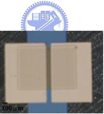
100μm and 1000μm, respsectively. The PMMA-OTFT structure and the optical
image are also shown in Fig.3-2.
In this study, all the experimental data were obtained from the semiconductor
parameter analyzer (HP 4156A) and impedance analyzer (HP 4284) in the dark at
room temperature.
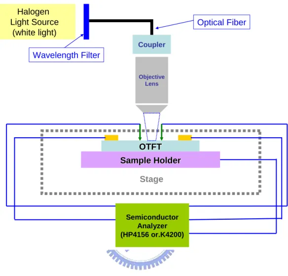
3-3 Photonic excitation
To study the effects of light-illumination on PMMA-OTFTs, we setup a probing
stage with a light-source, which is shown in Fig.3-3. The light-source we used in the
experiment is a 150W halogen lamp, which is filtered at 460nm by a band-pass filter
with a full width half maximum (FWHM) about 10nm. The filtered-light is guided
by an optical fiber and focused by a microscope. The total light power and the spot
diameter on the probing stage was about 1.5-2.7μW and 2.5mm, respectively. The
Chapter 4
Result and Discussion
4-1 Electrical properties of PMMA dielectric
4-1-1 Fabrication of PMMA dielectrics and relative dielectric properties
To fabricate a suitable capacitance for OTFTs, the dielectric thickness, roughness,
and leakage-current are important demands. In this experiment, we try to adjust the
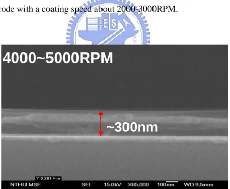
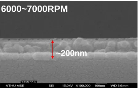
rotational speed of spin-on process to control the dielectric thickness. In Fig. 4-1(a),
(b), (c), we show the scanning electron microscope (SEM) images of PMMA
dielectrics on gate-electrode with different rotational speed. When the rotational
speed is increase from 2000 raid per minute (RPM) to 6000RPM, the PMMA
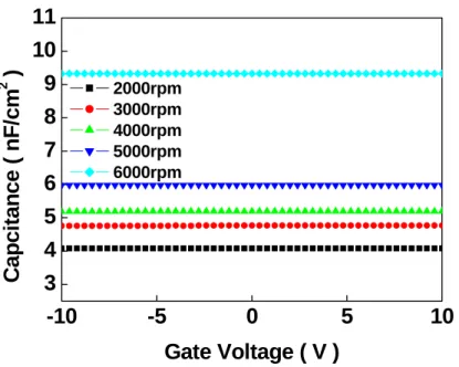
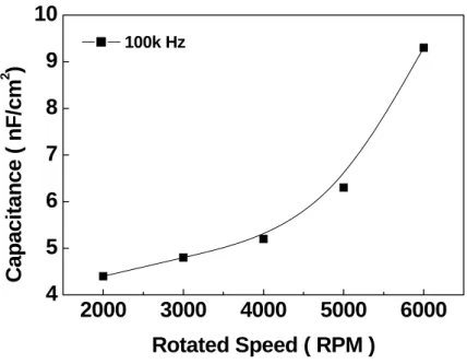
thickness will reduce from 500nm to 250nm. To further obtain the capacitance
values, all the PMMA dielectrics with different thickness are fabricated as the
metal-insulator-metal (MIM) structures for capacitance measurement. The measured
capacitance values from the impedance analyzer (Agilent 4284) indicate that the
capacitance will increase from 4nF/cm2 to 9.3nF/cm2 when the rotational speed
increase from 2000RPM to 6000RPM. The result is agreed with the estimate
dielectric thickness in SEM image and plotted as a capacitance-voltage (C-V) diagram
MIM structure. The leakage-current curves are plotted as a function of gate-voltage
in Fig. 4-3. As we can observe, the dielectric leakage is as low as 3×10⁻⁹ A/cm2
when the rotational speed remain lower than 5000RPM. When the rotational speed
is larger than 5000RPM, the dielectric leakage increases drastically to the level about
10-6 A/cm2. Therefore, if we consider a low-leakage PMMA dielectric with
maximum capacitance in this experiment, the rotational speed about 4000-5000RPM
should be the optimized value. All the C-V and leakage-current measurement are
summarized in Fig. 4-4(a) and (b), respectively.
4-1-2 UV- treatment on PMMA dielectric
We try to use the UV-treatment to change the functional groups on PMMA. In
the reported studies, it indicates that the UV-treatment on PMMA will result in the
formation of −COH as well as −COOH groups [23]. Besides, it is also reported
that the UV-treatment will create charged-sites on the polymer dielectrics and result in
the change of OTFT characteristics. In our experiment, the exposed time of PMMA
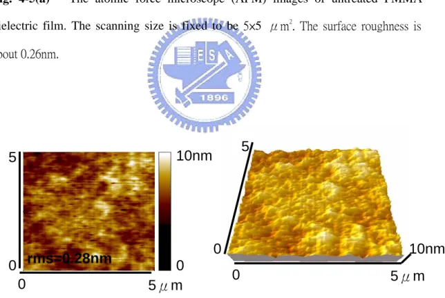
dielectric is about 60-90sec. The AFM images of untreated PMMA and UV-treated
PMMA is shown in Fig. 4-5(a) and (b), respectively. It reveals that the PMMA
roughness is not changed and remands around 0.2-0.3nm as well. Further more, we
II, the capacitance of untreated PMMA and UV-treated PMMA dielectric is
8.4nF/cm2 and 8.6nF/cm2, respectively. The leakage-current density at 1MV/cm is
3.4×10⁻⁹ A/cm2 for untreated PMMA dielectric and 3.6×10⁻⁹ A/cm2 for UV-treated
PMMA dielectric. It is evident that the UV-treatment on PMMA will not change its
surface and dielectric properties significantly.
4-2 Characteristics of OTFTs with distinct PMMA-dielectrics
In Fig. 4-6(a) and (b), we show the transfer characteristics of OTFT with
untreated PMMA dielectric and UV-treated dielectric, respectively. In OTFT with
untreated PMMA dielectric, the device shows a mobility about 0.24cm2/v-sec, a
threshold voltage about -6.8V, and a subthreshold swing about 0.9 V/decade. On the
other hand, the OTFT with UV-treated dielectric show a similar mobility about
0.21cm2/v-sec, a lower threshold voltage about -3.3V, and a larger subthreshold swing
about 1.8 V/decade. It is interesting that with the UV-treatment on dielectric, the
threshold voltage will be reduced and the subthreshold will be increased. But the
mobility almost remains unchanged. Further more, we try to estimate the
trap-density at the pentacene /PMMA interface from the subthreshold swing method.
It is found that the interface trap density is about 7.42x10¹¹ at untreated PMMA
UV-treatment on PMMA dielectric will create additional trap-sites. Besides, from
the change of threshold voltage, it imply that these UV-created sites may act as the
charged sites and influence the carrier concentration in OTFT channel region.
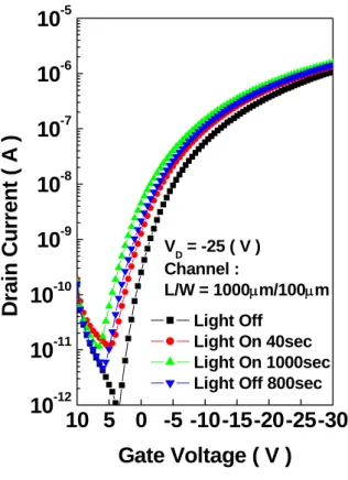
4-3 Characteristics of light-illumination on PMMA-OTFTs
In Fig. 4-7(a) and (b), we show the transfer characteristics of OTFT with
untreated PMMA dielectric under light-illumination. It reveals that turn-on current
increase and the threshold voltage shift toward more positively after the OTFT is
exposed to illumination. With the illumination-time increase up to about 1000 seconds, the threshold voltage shift (ΔVth ) reaches a value about 2V, and the
drain-current will increase from 9.96x10⁻⁷A to 1.39x10⁻⁶A. In Fig. 4-8(a) and (b),
we also show the transfer characteristics of OTFT with UV-treated PMMA dielectric
under light-illumination. Similar to the aforementioned results, the threshold voltage
will shift positively and the drain-current will increase after light-illumination.
However, in OTFT with UV-treated PMMA dielectric, the threshold voltage shift (ΔVth) approaches a larger value about 4V and the drain-current will increased from
1.09x10⁻⁶A to 1.57x10⁻⁶A. We also try to estimate the photo responsivity of the
OTFTs and plot the curves as a function of gate-voltage in Fig. 4-9(a) and 4-9(b).
seconds) of untreated-PMMA OTFT and UV-treated-PMMA OTFT is about 4.5A/W
and 6A/W, respectively. When the illumination time approaches 1000 seconds, the
photo responsivity is about 9A/W (in untreated-PMMA) and 11A/W (in UV-treated
PMMA). It is evident that PMMA-OTFT will show a larger photo responsivity
when the PMMA-dielectric is treated by the UV-light.
4-4 Time-dependent parameter analysis on PMMA-OTFTs under
and after light-illumination
Evidently, the mobility remains almost unchanged otherwise the
light-illumination is turned on and turned off. The subthreshold swing will slightly
increase under illumination and reduce to its original values, which is due to the
extraction method. Some studies indicate it is not significantly affected by the
illumination but an artifact, because the illumination will not change the density of
states in organic film [25]. The threshold voltage in UV-treated PMMA-OTFTs will
shift positively and rapidly about 2.7V and approach a saturated-value about 3.7V
when the illumination time is closed to 1000seconds. However, when the
illumination is turned off, the threshold voltage will return to its original value slowly.
On the other hand, the untreated PMMA-OTFTs show a smaller threshold shift about
1000seconds. To quantify the time-dependent threshold voltage shift (ΔVth), we try
to use the double exponential equation to describe the threshold voltage shift as a
function of time: 1 2 1 2 ( ) (1 ) (1 ) t t th V t V e τ V e τ − − Δ = ⋅ − + ⋅ − under light-illumination ' 1' ' 2' 1 2 ( ) t t th V t V e τ V e τ − − Δ = ⋅ + ⋅ illumination turned-off
Where the V , 1 V , 2 V , and 1' V are the fitting parameters; 2' τ1 and τ2 present the
“saturation time-constant” of threshold shift under light-illumination; ' 1
τ , and ' 2
τ present the “recovering time-constant” of threshold voltage after illumination is
turned off. The experimental data and the fitting-curves are plotted in Fig. 4-10(a)
and Fig.4-10(b) all the correspondent fitting parameters and time-constants are
summarized in Table III. As we can observe, two distinct time-constants can be
sufficient to fit the experimental data very well. One exhibits a rapid but minor
reaction with a shorter time-constant; the other exhibits a slow but major reaction with a longer time-time constant. We compare the “saturation time-constants” of ΔVth
between untreated and UV-treated PMMA-OTFTs under illumination. It is found that two OTFTs show similar shorter time-constants (τ1) around 30-40 seconds, but
show different longer time-constant (τ2 ) about 581 seconds for UV-treated
PMMA-OTFTs and 1001 seconds for untreated PMMA-OTFTs. We conclude that the UV-treated PMMA-OTFTs will show a larger ΔVth and shorter saturation
time-constant than that in untreated PMMA-OTFTs. On the other hand, both OTFTs
exhibit a shorter “recovering time-constants” ( ' 1
τ ) about 50-60 seconds. The longer
“recovering time-constants” ( ' 2
τ ) is about 712 seconds in untreated PMMA-OTFTs.
However, in UV-treated PMMA-OTFTs, the ' 2
τ is prolonged to 3687 seconds. It is
also conclude that the UV-treated PMMA-OTFTs show a smaller ΔVth recovering
and a longer recovering time-constant than that in untreated PMMA-OTFTs.
4-5 Material analysis on PMMA-OTFTs
Since the characteristics and response are much different in untreated and
UV-treated OTFTs, it is important to deduce the effects from UV-treatment. The
dielectric properties are almost the same, so we try to investigate the pentacene film
properties on different PMMA dielectric firstly. In Fig. 4-11(a) and Fig. 4-11(b), we
show the x-ray diffraction (XRD) curves of pentacene film on untreated and
UV-treated PMMA dielectrics. Both pentacene films show the (001) signal with a
peak value about 5.73° (degree) and a FWHM about 0.06° (degree). The higher
order signal of (002) and (003) peak is also observed with a values about 11.46°
(degree) and 17.21° (degree), respectively. According to the XRD analysis, it
implies that the pentacene films on untreated and UV-treated PMMA dielectrics are
pentacene crystal significantly. Consequently, we also try to verify the pentacene film
by the Raman spectrum. With the Raman analysis, the conformational transition
during carrier transport [26]. The pentacene vibration-modes of C−H (around
1155-1179cm-1) and C−C (around 1353-1380cm-1) bindings are plotted in Fig.
4-12(a) and (b) (from pentacene on untreated PMMA dielectric); (c) and (d) (from
pentacene on UV-treated PMMA dielectric). Both pentacene film show the similar
Raman shifts at 1158cm-1, 1179 cm-1, 1153 cm-1, and 1173 cm-1. The result also
reveals that the intermolecular coupling will not be changed even if the pentacene
film is deposited on untreated or UV-treated PMMA dielectric. Finally, we also
show the absorption spectrum of the two pentacene films on different PMMA
dielectrics. Once again, two pentacene film have almost identical absorption
properties. Base on these material analyses, the crystalline, molecular coupling, and
the absorptive properties of pentacene film on these distinct PMMA dielectrics should
be almost identical.
In order to verify the property of dielectric trapping, we try to observe the
time-dependent leakage current on these two PMMA dielectrics. It had been
investigated that when the dielectric trapping appears in the gate-insulator. The
leakage-current will be a function of time and approach to a saturated value when the
time-dependent leakage-current of untreated and UV-treated PMMA, respectively. It
is evident that both leakage-currents are almost kept at a constant level about 2×10⁻⁹
A/cm2 and will not change with time, event if these dielectrics are stress at a reversed
gate bias-stress about -20V. Hence, we conclude that the dielectric trapping is not
significant in these two PMMA dielectrics.
4-6 Plausible origin of the enhancement on photo responsivity
The material analyses have shown that the pentacene film and the dielectric
properties are almost alike in these two PMMA-OTFTs. It is probable the
differences of OTFT transfer characteristic and its photo responsivity are originate
from the interface traps, which are created by the UV-light treatment. These
UV-created interface traps should be act as negative sites, which may withdraw the
electrons but accumulate the holes in pentacen film, near the interface of pentacene
and PMMA dielectrics (UV-treated). Hence, the hole-accumulation will result in an
upward-bended HOMO-band and build up an internal electric field near the interface.
When the PMMA-OTFTs are illuminated, the electron-hole pairs will be generated in
the pentacene film. In UV-treated PMMA-OTFTs with build-in electric field, holes
will be swept toward the PMMA-dielectric and the electrons will be swept toward
come about faster than the case in untreated PMMA-OTFTs. Interestingly, from the
analysis of saturation time-constant, the UV-treated PMMA-OTFTs show a smaller
total saturation time than the untreated PMMA-OTFTs. It reveals that the process of
threshold-voltage shift is faster in the UV-treated PMMA OTFTs. The result is good
agreed with the assumption. Consequently, if the light-irradiation is removed, the
electrons and holes begin to recombine. In the UV-treated PMMA-OTFTs, with a
build–in electric field, the spatial separation between electrons and holes will be
longer than that in untreated PMMA-OTFTs. As a result, the recombination rate will
be reduced and show a prolonged recovering time. Therefore, we deduced from the
recovering time-constant. Significantly, the total recovery time-constant is longer in
UV-treated PMMA OTFTs than that in untreated PMMA OTFTs. Again, the result is
good agreed to the proposed model. The correspondent model can be explained by
the band-diagram and plotted in Fig. 4-14 (a), (b), (c), and (d). Furthermore, to
verify the proposed assumption, we try to extract the saturation time-constant and the
recovering time-constant of photo-generated current, as a function of gate-voltage.
The extraction equation is identical to the time-dependent threshold voltage shift:
1 2 1 2 I ( ) (1 ) (1 ) t t photo t I e I e τ τ − − = ⋅ − + ⋅ − under light-illumination ' 1' ' '2 1 2 I ( ) t t photo t I e I e τ τ − − = ⋅ + ⋅ illumination turned-off
the “saturation time-constant” of threshold shift under light-illumination; ' 1
τ , and ' 2
τ present the “recovering time-constant” of threshold voltage after illumination is
turned off. In Fig. 4-15(a) is the Saturation time-constant as a function of gate voltage. When the gate voltage increase, τ1 is almost the same but τ2 will decrease
in untreated and UV-treated PMMA-OTFTs. In Fig.4-15(b) is Recovering
time-constant as a function of gate voltage. When the gate voltage increase, ' 1
τ is
almost the same but ' 2
τ will increase in untreated and UV-treated PMMA-OTFTs.
Since the higher gate-voltage will produce larger band bending and increase the
internal electric field near the interface of organic semiconductor and gate-dielectric.
Evidently, a larger upward bending will reduce the saturation time-constant and
prolong the recovering time-constant. All the results are agreed with the assumption
of build-in electric field. Base on these experimental results, we may conclude that
the UV-treated PMMA, which may create additional interface traps, should be the
origin of these distinct responses in PMMA-OTFTs. The proposed “build-in electric
Chapter 5
Conclusion
5-1 Conclusion
In this study, we try to fabricate the OTFTs with solution-based PMMA
gate-dielectrics and investigate the effects of UV-light treatment on PMMA
gate-dielectrics. With the UV-light treatment, the threshold voltage and the
subthreshold swing will be significantly altered, but the field-effect mobility remains
almost unchanged. When the light-irradiation on these OTFTs, the devices with
UV-light treatment will show a larger threshold voltage shift and a larger photo
responsivity than those devices without UV-light treatment. In order to investigate
the effect of UV-light treatment on OTFTs characteristics, the material analysis and
the dielectric leakage-current measurement are proceeded. It is found that the
variation of the semiconductor layer and the trapping in the dielectric layer should
not be the dominated factors. By the time-dependent analysis of threshold voltage
shift and photo-generated current, the saturated time and the recovering time show a
strong correlation to the gate-voltage. That implies the electric-field in the organic
semiconductor film will influence the behavior drastically. It is most probably the
PMMA-dielectric and the organic semiconductor, which will result in a build-in
electric-field in the organic semiconductor near the PMMA gate-dielectric. Hence,
the OTFTs with UV-light treatment will show different characteristics, such as a
References
[1] A. Tsumura, K. Koezuka, and T. Ando, “Macromolecular electronic devices: Field-effect transistor with a polythiophene thin film”, Appl. Phys. Lett. vol.49, pp. 1210, (1986).
[2] J. H. Burroughes, C. A. Jones, and R. H. Friend, “Polymer diodes and transistors: new semiconductor device physics”, Nature, vol. 335, pp.137, (1988).
[3] Y. Y. Lin, D. J. Gundlach, S. F. Nelson, and T. N. Jackson, “Pentacene organic thin-film transistors-molecular ordering and mobility”, IEEE Electron Device Lett. vol. 18, pp. 87, (1997).
[4] H. Sirringhaus, R. J. Wilson and R. H. Friend, ” Mobility enhancement in conjugated polymer field-effect transistors through chain alignment in a liquid-crystalline phase”, Appl. Phys. Lett. Vol.77, pp.406, (2000).
[5] W. Y. Chou, and H. L. Cheng, “An Orientation-Controlled Pentacene Film Aligned by Photoaligned Polyimide for Organic Thin-Film Transistor Applications”, Adv. Funct. Mater. , vol. 14, pp. 811, (2004).
[6] Tobat P. I. Saragi, Robert Pudzich, Thomas Fuhrmann-Lieker, and Josef Salbeck, “Ultraviolet-sensitive field-effect transistor utilized amorphous thin films of organic donor/acceptor dyad”, Appl. Phys. Lett., vol. 90, pp. 143514, (2007). [7] Zheng-Tao Zhu, Jeffrey T. Mason, Rüdiger Dieckmann, and George G. Malliaras,
“Humidity sensors based on pentacene thin-film transistors”, Appl. Phys. Lett., vol. 81, pp. 4643, (2002).
[8] Jeong-M. Choi, Jiyoul Lee, D. K. Hwang, Jae Hoon Kim, and Seongil Im, “Comparative study of the photoresponse from tetracene-based and pentacene-based thin-film transistors”, Appl. Phys. Lett. Vol. 88, pp. 043508,
(2006).
[9] De Angelis, F.; Toccoli, T.; Pallaoro, A.; Coppedè, N.; Mariucci, L.; Fortunato, G.; Iannotta, S., “SuMBE based organic thin film transistors”, Synth. Met., vol. 146, pp. 291, (2004).
[10] Hagen Klauk, Marcus Halik, Ute Zschieschang, Günter Schmid, and Wolfgang Radlik, “High-mobility polymer gate dielectric pentacene thin film transistors”, J. Appl. Phys., vol. 92, pp.5259, (2002).
[11] Yusaku Kato, Shingo Iba, Ryohei Teramoto, Tsuyoshi Sekitani, and Takao Someya, ” High mobility of pentacene field-effect transistors with polyimide gate dielectric layers”, Appl. Phys. Lett. , vol.84, pp.3789, (2004).
[12] F. De Angelis, S. Cipolloni, L. Mariucci, and G. Fortunato, “High-field-effect-mobility pentacene thin-film transistors with polymethylmetacrylate buffer layer”, Appl. Phys. Lett., vol. 86, pp. 203505, (2005).
[13] Yanming Sun, Yunqi Liu, and Daoben Zhu, “Advances in organic field-effect transistors”, J. Mater. Chem., vol. 15, pp. 53, (2005).
[14] R. A. Street, D. Knipp, and A. R. Völkel, “Hole transport in polycrystalline pentacene transistors”, Appl. Phys. Lett., vol. 80, pp. 1658, (2002).
[15] G. Horowitz, “Organic field-effect transistors”, Adv. Mater., vol. 10, pp. 365, (1998).
[16] Y.-Y. Lin, D. J. Gundlach, S. F. Nelson, and T. N. Jackson, “Stacked pentacene layer organic thin-film transistors with improved characteristics”, IEEE Electron Device Lett, vol. 18, pp 606, (2000).
[17] Y.-Y. Lin, D. J. Gundlach, S. F. Nelson, and T. N. Jackson, “Stacked pentacene layer organic thin-film transistors with improved characteristics”, IEEE Electron
[18] S. F. Nelson, Y.-Y. Lin, D. J. Gundlach, and T. N. Jackson, “Temperature-independent transport in high-mobility pentacene transistors”, Appl. Phys. Lett., vol. 72, pp. 1854, (1998).
[19] U. Zschieschang, H. Klauk, M. Halik, G. Schmid, C. Dehm, “Flexible Organic Circuits with Printed Gate Electrodes”, Adv. Mater., vol. 15, pp 1147, (2003). [20] J. Z. Wang, J. Gu, F. Zenhausern, and H. Sirringhaus, “Low-cost fabrication
of submicron all polymer field effect transistors”, Appl. Phys. Lett., vol. 88, pp. 133502, (2006).
[21] Sang Yoon Kwonwoo, Kwonwoo Shin, and Chan Eon Park, “The Effect of Gate-Dielectric Surface Energy on Pentacene Morphology and Organic Field-Effect Transistor Characteristics”, Adv. Funct. Mater., vol. 15, pp. 1806, (2005).
[22] Pyo, Kyung Soo; Song, Chung Kun, “The effects of simultaneous treatment of SiO2 gate and Au electrode with octadecyltrichlorosilane and charge transfer molecules on characteristics of pentacene thin film transistors”, Thin Solid Film, vol. 485, pp. 230, (2005).
[23] A. Torikai, M. Ohno, and K. Fueki, “Photodegradation of Poly(methyl Methacrylate) by Monochromatic Light:Quantum Yield, Effect of Wavelengths, and Light Intensity”, J.Appl. polym. Sci., vol 41, pp. 1023, (1990).
[24] Lay-Lay Chua, Jana Zaumseil, Jui-Fen Chang, Eric C.-W. Ou, Peter K.-H. Ho, Henning Sirringhaus, Richard H. Friend, “General observation of n-type field-effect behaviour in organic semiconductors”, Nature., vol 434, pp. 194 (2005).
[25] Hamilton, M.C.; Martin, S.; Kanicki, J., “Thin-film organic polymer phototransistors”, IEEE Trans., vol. 51, pp. 877, (2004).
[26] Horng-Long Cheng, Yu-Shen Mai, Wei-Yang Chou, and Li-Ren Chang,
“Influence of molecular structure and microstructure on device performance of polycrystalline pentacene thin-film transistors”, Appl. Phys. Lett., vol. 90, pp. 171926, (2007).
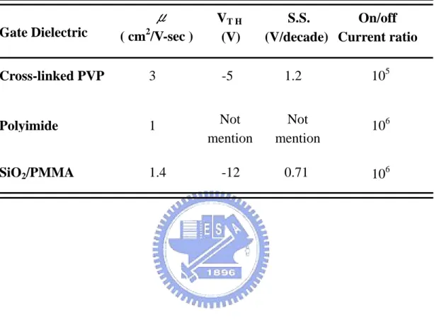
Table I The comparison of the different polymer OTFTs electrical properties Gate Dielectric
μ
( cm2/V-sec ) VT H (V) S.S. (V/decade) Cross-linked PVP 3 -5 1.2 On/off Current ratio 105 Polyimide SiO2/PMMA 1.4 -12 0.71 106 106 1 Not mention Not mentionTable II The comparison of untreated and UV-treated PMMA dielectrics properties
Untreated
UV-treated
Capacitance
(nF/cm
2)
8.43
8.64
Leakage (A/cm
2)
@ 1MV/cm
3.43x10
-93.66x10
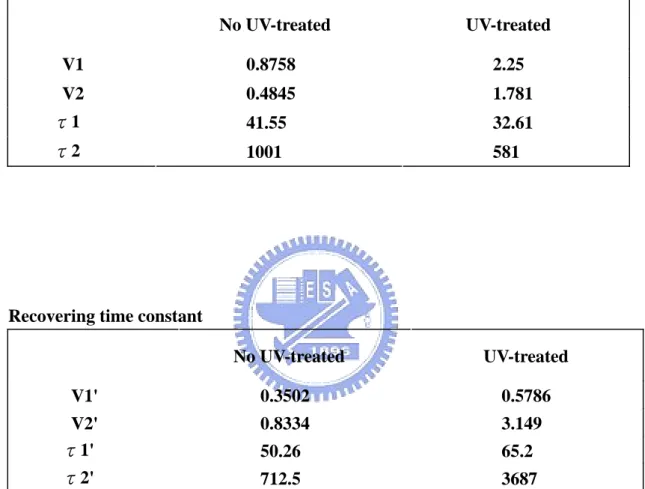
-9Table III Time dependent analysis on PMMA-OTFT parameter
Saturation time constant
No UV-treated UV-treated
V1 0.8758 2.25
V2 0.4845 1.781
τ1 41.55 32.61
τ2 1001 581
Recovering time constant
No UV-treated UV-treated
V1' 0.3502 0.5786
V2' 0.8334 3.149
τ1' 50.26 65.2
Fig. 3-1 The cross-section of PMMA-OTFT device.
Fig. 3-2 The optical image of PMMA-OTFT.
glass
Pd/Ni
PMMA
Pentacene
Au Au
100μm
Fig. 3-3 The experimental diagram of probing stage with a light source.
Sample Holder Sample Holder OTFT OTFT Semiconductor Analyzer (HP4156 or.K4200) Stage Objective Lens Halogen Light Source (white light) Wavelength Filter Coupler Optical Fiber
Fig. 4-1(a) The scanning electron microscope (SEM) image of PMMA-dielectrics on gate-electrode with a coating speed about 2000-3000RPM.
Fig. 4-1(b) The scanning electron microscope (SEM) image of PMMA-dielectrics on gate-electrode with a coating speed about 4000-5000RPM.
4000~5000RPM
~300nm
2000~3000RPM
Fig. 4-1(c) The scanning electron microscope (SEM) image of PMMA-dielectrics on gate-electrode with a coating speed about 6000-7000RPM.
6000~7000RPM
Fig. 4-2 Capacitance-voltage (C-V) measurement of PMMA-dielectrics with different rotated speed.
Fig. 4-3 The leakage-current density versus the electri- field (J-E) plot of different PMMA dielectrics, which are fabricated with different rotated speed.
-10 -5 0 5 10 3 4 5 6 7 8 9 10 11 C a p c it an ce ( nF /c m 2 ) Gate Voltage ( V ) 2000rpm 3000rpm 4000rpm 5000rpm 6000rpm 0.0 0.2 0.4 0.6 0.8 1.0 10-12 10-11 10-10 10-9 10-8 10-7 10-6 Leakage Cur rent ( A /cm 2 ) Electric Field ( MV/cm2 ) 2000rpm 3000rpm 4000rpm 5000rpm 6000rpm
Fig. 4-4(a) Capacitance value of PMMA-dielectric is plotted as a function of rotated-speed and measured at a frequency of 100kHz.
Fig. 4-4(b) Leakage-current of PMMA-dielectric is plotted as a function of rotated-speed and measured at different vertical electric field: 0.4MV/cm, 0.7 MV/cm, and 1MV/cm, respectively. 2000 3000 4000 5000 6000 4 5 6 7 8 9 10 Capac it a nc e ( nF/ c m 2 ) Rotated Speed ( RPM ) 100k Hz 2000 3000 4000 5000 6000 10-9 10-8 10-7 10-6 Leakage Cur rent ( A /cm 2 ) Spin Speed ( RPM ) @0.4MV/cm @0.7MV/cm @1MV/cm
Fig. 4-5(a) The atomic force microscope (AFM) images of untreated PMMA dielectric film. The scanning size is fixed to be 5×5 μm2. The surface roughness is about 0.26nm.
Fig. 4-5(b) The atomic force microscope (AFM) image of UV-treated PMMA dielectric film. The scanning size is fixed to be 5×5 μm2. The surface roughness is
5
0 10nm
5μm
0
0
0 0
5
5μm
10nm
0
0 0
0
0
5
5
5μm
5μm
10nm
10nm
rms=0.26nm
rms=0.28nm
Fig. 4-6(a) Transfer characteristics of OTFT with untreated PMMA dielectric.
10
0
-10
-20
-30
-40
10
-1310
-1210
-1110
-1010
-910
-810
-710
-610
-50.0
0.5
1.0
1.5
2.0
2.5
3.0
3.5
Channel : L/W = 100μm/1000μmDr
ai
n Cur
re
nt
(
A
)
Gate Voltage ( V )
VD = -5 ( V ) VD = -25 ( V )( Dr
ai
n Cur
re
nt
)
1/ 2( m
A
)
1/210
0
-10
-20
-30
-40
10
-1210
-1110
-1010
-910
-810
-710
-610
-50.0
0.5
1.0
1.5
2.0
2.5
3.0
3.5
Channel : L/W = 100μm/1000μmDr
ai
n Cur
re
nt
(
A
)
Gate Voltage ( V )
VD = -5 ( V ) V D = -25 ( V )( Dr
ai
n Cur
re
nt
)
1/ 2( m
A
)
1/2Fig. 4-7(a) The semi-log diagram of transfer characteristics of light-illumination on PMMA-OTFTs (untreated PMMA dielectric).
Fig.4-7(b) The linear diagram of transfer characteristics of light-illumination on
10 5 0 -5 -10-15-20-25-30 10-13 10-12 10-11 10-10 10-9 10-8 10-7 10-6 10-5 V D = -25 ( V ) Channel : L/W = 1000μm/100μm Dr a in Cur re nt ( A ) Gate Voltage ( V ) Light Off Light On 40sec Light On 1000sec Light Off 800sec
10 5 0 -5 -10-15-20-25-30 0.0 0.2 0.4 0.6 0.8 1.0 1.2 1.4 ( Dr ai n Cur rent ) 1/ 2 ( m A ) 1/ 2 Gate Voltage ( V ) Light Off Light On 40sec Light On 1000sec Light Off 800sec
Fig.4-8(a) The semi-log diagram of transfer characteristics of light-illumination on PMMA-OTFTs (UV-treated PMMA dielectric).
Fig. 4-8(b) The linear diagram of transfer characteristics of light-illumination on
10 5 0 -5 -10-15-20-25-30 0.0 0.2 0.4 0.6 0.8 1.0 1.2 1.4 ( Dr ai n Cur rent ) 1/ 2 ( m A ) 1/ 2 Gate Voltage ( V ) Light Off Light On 40sec Light On 1000sec Light Off 800sec
10 5 0 -5 -10-15-20-25-30 10-12 10-11 10-10 10-9 10-8 10-7 10-6 10-5 VD = -25 ( V ) Channel : L/W = 1000μm/100μm Dr a in Cur re nt ( A ) Gate Voltage ( V ) Light Off Light On 40sec Light On 1000sec Light Off 800sec
Fig. 4-9(a) Photo responsivity is plotted as a function of gate-voltage of the untreated OTFT (illumination time is 40s to1000s).
Fig. 4-9(b) Photo responsivity is plotted as a function of gate-voltage of the 0 -5 -10 -15 -20 -25 -30 0 2 4 6 8 10 12 UV-exposed PMMA Illumination Power : 45μW/cm2 R e s p o n s iv ity ( A /W ) Gate Voltage ( V ) 0 -5 -10 -15 -20 -25 -30 0 2 4 6 8 10 12
None UV-exposed PMMA Illumination Power : 45μW/cm2 R e s ponsi v it y ( A /W ) Gate Voltage ( V )
Fig. 4-10(a) The experimental data and the fitting-curves of threshold voltage shift is plotted as a function of time, when the PMMA-OTFTs are illuminated with light.
Fig. 4-10(b) The experimental data and the fitting-curves of threshold voltage shift
0 200 400 600 800 10001200 0 1 2 3 4 Δ V th ( V ) Time ( Sec ) No UV Rising UV Rising Fitting Line 12000 1400 1600 1800 2000 1 2 3 4 Δ V th ( V ) Time ( Sec ) No UV Decay UV Decay Fitting Line
Fig. 4-11(a) The X-ray diffraction (XRD) curves of pentacene film on untreated PMMA dielectric.
Fig. 4-11(b) The X-ray diffraction (XRD) curves of pentacene film on UV-treated PMMA dielectric. 5 10 15 20 5 10 15 20 ( 003 ) 17.210, FWHM:0.0730 ( 002 ) 11.460, FWHM:0.0640 ( 001 ) 5.730, FWHM:0.0620 2θ ( Degree ) XRD data None-UV Pentacene X R D In te n s ity ( a .u . ) 2θ ( Degree ) Fitting Line 5 10 15 20 5 10 15 20 ( 003 ) 17.2350, FWHM:0.0790 ( 002 ) 11.470, FWHM:0.0670 ( 001 ) 5.7350, FWHM:0.061450 2θ ( Degree ) XRD data
UV
X R D In te n s ity ( a .u . ) 2θ ( Degree ) Fitting LineFig. 4-12(a) The Raman spectrum (1140-1200cm-1) of pentacene film on untreated PMMA dielectric.
Fig. 4-12(b) The Raman spectrum (1320-1400cm-1) of pentacene film on untreated PMMA dielectric. 1140 1160 1180 1200 0 100 200 300 400 500 600 1140 1160 1180 1200 0 100 200 300 400 500 600 1140 1160 1180 1200 0 100 200 300 400 500 600 1140 1160 1180 1200 0 100 200 300 400 500 600 1140 1160 1180 1200 0 100 200 300 400 500 600 1140 1160 1180 1200 0 100 200 300 400 500 600 1140 1160 1180 1200 0 100 200 300 400 500 600 In te n s ity ( a .u . ) Raman Shift ( cm-1 ) Origin Raman Shift ( cm-1 ) SUM P1 P2 P3 P4 P5
Pentacene on none-UV PMMA
1320 1340 1360 1380 1400 0 100 200 300 400 500 600 700 800 1320 1340 1360 1380 1400 0 100 200 300 400 500 600 700 800 Pentacene on none-UV-PMMA Raman Shift ( cm-1 ) Data In te n s ity ( a .u . ) Raman Shift ( cm-1 ) D E F G
Fig. 4-12(c) The Raman spectrum (1140-1200cm-1) of pentacene film on UV-treated PMMA dielectric.
Fig. 4-12(d) The Raman spectrum (1320-1400cm-1) of pentacene film on UV-treated PMMA dielectric.
1140 1160 1180 1200 0 100 200 300 400 1140 1160 1180 1200 0 100 200 300 400 1140 1160 1180 1200 0 100 200 300 400 1140 1160 1180 1200 0 100 200 300 400 1140 1160 1180 1200 0 100 200 300 400 1140 1160 1180 1200 0 100 200 300 400 1140 1160 1180 1200 0 100 200 300 400 In te n s ity ( a .u . ) Raman Shift ( cm-1 ) Origin Raman Shift ( cm-1 ) SUM P1 P2 P3 P4 P5 Pentacene on UV PMMA 1320 1340 1360 1380 1400 0 100 200 300 400 500 600 1320 1340 1360 1380 1400 0 100 200 300 400 500 600 Pentacene on UV-PMMA Raman Shift ( cm-1 ) Data In te n s ity ( a .u . ) Raman Shift ( cm-1 ) D E F G
Fig. 4-13(a) The leakage-current of untreated PMMA dielectric is plotted as a function of time.
Fig. 4-13(b) The leakage-current of UV-treated PMMA dielectric is plotted as a function of time. 0 50 100 150 200 250 300 1.0x10⁻⁹ 2.0x10⁻⁹ 3.0x10⁻⁹ 4.0x10⁻⁹ Leakag e C u rren t ( A /cm 2 ) Time ( Sec ) 1st measurement 2nd measurement
After stress (20V 10mins)
0 50 100 150 200 250 300 1.0x10⁻⁹ 2.0x10⁻⁹ 3.0x10⁻⁹ 4.0x10⁻⁹ Leakag e C u rren t ( A /cm 2 ) Time ( Sec ) 1st measurement 2nd measurement