立體超緊耦合結構之研究與其在寬頻耦合器與帶通濾波器的應用
64
0
0
全文
(2) 立體超緊耦合結構之研究與其在寬頻耦合器與 帶通濾波器的應用 Three-Dimensional Extremely Tight Coupling Structures and Their Application on Broadband Coupler and Bandpass Filter 研究生:陳慧諄. Student: Hui-Chun Chen. 指導教授:張志揚 博士. Advisor: Dr. Chi-Yang Chang. 國立交通大學 電信工程學系 博士論文 A Dissertation Submitted to Institute of Communication Engineering College of Electrical and Computer Engineering National Chiao Tung University in Partial Fulfillment of the Requirements for the Degree of Doctor of Philosophy in Communication Engineering Hsinchu, Taiwan 2008 年 1 月.
(3) 立體超緊耦合結構之研究與其在寬頻耦合 器與帶通濾波器的應用 學生:陳慧諄. 指導教授:張志揚. 博士. 國立交通大學 電信工程學系 摘要 本論文主要在研究立體超緊耦合結構,以及其在寬頻耦合器與 帶通濾器上的應用。其中所提的二種新型立體超緊耦合結構是一 種在兩旁有介質方塊的垂直基板平面電路結構。運用所提此二種 耦合結構,我們可以解決實現超寬頻多節串接式混成器所面臨的 超緊耦合量、奇偶模模態速度不等與不連續接面等挑戰。在適當 的設計之下,我們可以實現一個效能極佳的超寬頻混成器。經由 進一步的變化,我們提出並且分析另外二種濾波器結構分別是垂 直基板平面電路步階阻抗諧振器與懸置基板帶線步階阻抗諧振 器。此二種諧振器所構成的帶通濾波器結構可以實現濾波器具有 寬的通帶頻寬(大於二比一)、好而且寬的上止帶表現但是只須要 使用一般的印刷電路板製程技術。對於所提結構有詳細的特性敘 訴與分析,並且介紹系統化的設計流程以及其在實例上的驗證。. I.
(4) Three-Dimensional Extremely Tight Coupling Structures and Their Application on Broadband Coupler and Bandpass filter Student: Hui-Chun Chen. Advisor: Dr. Chi-Yang Chang. Department of Communication Engineering National Chiao Tung University Abstract This dissertation presents the research and applications of three-dimensional extremely tight coupling structures. Two of them are the modified vertically installed planar structures with dielectric block at both side of vertical substrate. With these two newly proposed structures, we have overcome the three main challenges in realization of ultra-broadband multi-section quadrate hybrid. The challenges are to obtain an extremely tight coupling value, to compensate the unequal even- and odd-mode modal phase velocitys, and to minimize the discontinuous effect at junctions. Thanks to the proposed structures a five-section ultra-broadband quadrate hybrid with excellent performance is realized. Extending the application of tight coupling structures to broadband filters, two stepped impedance resonator (SIR) structures are proposed. The proposed SIR structures are the vertically installed planar stepped impedance resonator (VIPSIR) and the suspended substrate stripline stepped impedance resonator (SSSSIR). These two filter structures can realize bandpass filters with broad passband of larger than 1:2, good and wide upper stopband performance. More importantly, conventional PCB process can be applied to mass produce II.
(5) both filters. The analysis procedures and the characteristics of the proposed structures are described in detail. Moreover, systematical design procedures are given and proved to be valid with several experimental examples in this dissertation.. III.
(6) 謝誌. 首先要感謝張志揚教授在這六年多辛勤與耐心的指導,每當我 陷入研究的困境時都能適時的激勵、啟發與指正,帶我走出迷惘, 也使得本論文可以完成。另外也感謝口試委員鍾世忠教授、林育 德教授、郭仁財教授、邱煥凱副教授與湯敬文副教授對於本論文 研究所給予的指正與意見。 這裡也要感謝微波實驗室的學長、弟、妹們多年的照顧。特別 是正中、士鳴、竟谷與鈞翔在此其間所給與的意見與鼓勵。最後 在此感謝我的家人、妻子、同事在此期間對我的支持與鼓勵。. 慧諄 2008 年一月於台灣新竹 IV.
(7) Contents Abstract (Chinese)……………………………………………………………………………I Abstract……………………………………………………………………………………….II Acknowledgement………………………………………………………………………….III Contents…………………………………………………………………………………….IV List of Tables………………………….………………………………………………………VI List of Figures………………………………………………………………………………VII 1. Intorduction……………………………………………………………………………1 1.1 Coupled structures……………………………………………………………………2 1.2 Motivation…………………………………………………………………………..5 1.3 Chapter outline………………………………………………………………………9. 2. Analysis and Characteristic of Proposed Structure......................................................10 2.1 Analysis and characteristic of proposed modified VIP coupled lines……………10 2.2 Structures of proposed VIPSIR and SSSSIR………………………………………14 2.3 Analysis and characteristic of proposed filter structure…………………………..16 2.4 Characteristics of filter structure A…………………………...……………..16 2.5 Characteristics of filter structure B…………………………………………20. 3. Analysis, Design and Realization of Ultra-Broadband Multi-Section Quadrature Hybrid……………………..……………………………………………………………..25 3.1 Literature survey………………………………………………………………….25 3.2 Theory and design procedures………………………………………………………26 V.
(8) 3.3 Ultra-broadband multi-section quadrature hybrid using modified VIP coupler.........31 4. Analysis, Design and Realization of Broadband Bandpass Filters with Wide Upper Stopband Using Parallel-coupled VIPSIRs and SSSIRs...............................................34 4.1 Literature survey………………………………………………………………...….34 4.2 Filter design procedures…………………………………………………………….36 4.3 Simulation and measurement………………………………………………………..38 4.4 Simulation and measurement using VIPSIR………………………………….38 4.5 Simulation and measurement using SSSSIR………………………………..43. 5. Conclusions……………………………………………………………………………..45. Reference…………………………………………………………………………………….47. VI.
(9) List of Tables Table 3.1 Design parameters and physical dimensions of experimental coupler…………….31 Table 4.1 Specifications and dimensions of the experimental filters of structure A………….38 Table 4.2 Specifications and dimensions of the experimental filters of Filter structure B…...43. VII.
(10) List of Figures Fig. 1.1 Edged-coupled microstrip lines (a) cross-sectional view (b) top view…….………….3 Fig. 1.2 Enhanced edge-coupled structures of (a)-(b) re-entrant coupled lines and (c)-(d) Lange coupler. ……………………………………………………………………....4 Fig. 1.3 Broadside coupled transmission: (a) Broadside coupled suspended microstrip lines. (b) Offset broadside coupled suspended microstrip lines………………………………4 Fig. 1.4 Cross-sectional view of a conventional VIP coupling structure…………………….5 Fig. 1.5 Three-dimensional view of proposed modified VIP structure coupling structures (a) type I with dielectric overlays for moderate coupling, and (b) type II with dielectric overlays and finite-extent ground plan for extremely tight coupling………………..7 Fig. 1.6 The proposed filter resonator structures. (a) Structure A use the vertically installed planar stepped impedance resonator, and (b) structure B adopts the suspended substrate stripline stepped impedance resonator (SSSSIR)………………………….8 Fig. 2.1 Cross-sectional views of (a) type I, and (b) type II of the modified VIP couplers, where H sub =0.508mm, W VIP =0.2032mm, H VIP =3.048mm, W DR =5.08mm, Wgnd=0.381mm, HDR=1.524mm, and εr1=εr2=εr3=3.38…………………………..…11 Fig. 2.2 Even- and odd-mode characteristic impedances versus VIP metal height (Hmetal) of the type I VIP coupler with (a) G=0.4572mm, and (b) G=0.7112mm……….…….12 Fig. 2.3 (a) even- and odd-mode characteristic impedances, and (b) effective dielectric constants versus Ggnd and Hmetal of the type II VIP coupler……………………….13 Fig. 2.4 The proposed filter structures. (a) Structure A where the vertically installed planar stepped-impedance resonators are used, and (b) structure B where the modified stripline stepped-impedance resonators are used…………...………………………14 Fig. 2.5 Equivalent circuit for structure A and B in Fig. 2.4, where P-P’ is the symmetrical plane.……………………………………………………………………………..15 VIII.
(11) Fig. 2.6 Cross-sectional views of filter structure A. (a) vertically installed planar-coupled line, and (b) high impedance uncoupled line, where Hsub=0.508mm, HVIP=0.2032mm, WHZ=0.254mm, WVIP=3.048mm, and єr1=єr2=3.38 are chosen in this paper…….…17 Fig. 2.7 (a) Even-mode and (b) Odd-mode characteristic impedances versus strip width (WLZ) on the vertical substrate with various patch width (W) on the main substrate, where H s u b =0.508mm, H V I P =0.2032mm, W H Z =0.254mm, W V I P =3.048mm, and єr1 =єr2=3.38………………………………………………………………………18 Fig. 2.8 (a) Even-mode and (b) Odd-mode effective dielectric constants versus strip width (WLZ) on the vertical substrate with various patch width (W) on the main substrate, where Hsub =0.508mm, HVIP=0.2032mm, W HZ=0.254mm, WVIP=3.048mm, and є r1 =є r2 =3.38……………………………………………………………..………19 Fig. 2.9 Effective dielectric constant and characteristic impedance versus the distance (DHZ) between high impedance line and the main substrate where the strip width WHZ on the vertical substrate is fixed to be 0.254mm, Hsub=0.508mm, HVIP=0.2032mm, WVIP=3.048mm, and єr1=єr2=3.38…………………………………………………20 Fig. 2.10 Cross-sectional views of the filter structure B. (a) broadside-coupled line, and (b) high impedance uncoupled line, where H 1 =0.508mm, H 2 =0.2032mm, WHZ=0.2032mm, єr1=єr2=3.38, and P-P’ is the symmetrical plane…………………21 Fig. 2.11 (a) Even-mode and (b) Odd-mode characteristic impedances versus ground plane aperture size (Ggnd ) with various broadside coupled-line width (W), where H1=0.508mm, H2=0.2032mm, WHZ=0.2032mm, and єr1=єr2=3.38...................…….22 Fig. 2.12 (a) Even-mode and (b) Odd-mode effective dielectric constants versus ground plane aperture size (Ggnd) with various broadside coupled-line widths (W), where H1=0.508mm, H2=0.2032mm, WHZ=0.2032mm, and єr1=єr2=3.38…………….23 Fig. 2.13 Effective dielectric constant and characteristic impedance versus the ground plane aperture size (Ggnd), where H1=0.508mm, H2=0.2032mm, WHZ=0.2032mm, and IX.
(12) єr1=єr2=3.38……………………………………….………………………………24 Fig. 3.1 Schematic circuit representation of a single-section coupler………………………..26 Fig. 3.2 Schematic circuit expression of coupler with (a) even mode excitation and (b) odd mode excitation…….…………………………………………………………….27 Fig. 3.3 A N-section cascaded symmetrical quadrature hybrid……………………………..29 Fig. 3.4 Photograph of the fabricated five-section 3dB directional coupler………………….31 Fig. 3.5 Simulated responses of the proposed hybrid………………………………………32 Fig. 3.6 Measured responses of the proposed hybrid………………………………………..32 Fig. 3.7 Measured and simulate amplitude and phase errors of the proposed hybrid………..33 Fig. 4.1 Simulated and measured responses of filter A…………………………………….39 Fig. 4.2 Simulated and measured responses of filter B……………………………………40 Fig. 4.3 A sketch drawing for filter D. A high impedance microstrip line is used to connect two VIP substrates. The numbers on the mail substrate indicate the section number in Table 4.1.……………..………………………………………………………….40 Fig. 4.4 Simulated and measured responses for filter C…………………………………….41 Fig. 4.5 Simulated and measured responses for filter D…………………………………….42 Fig. 4.6 Photographs of proposed (a) filter A and (b) filter B……………………………….42 Fig. 4.7 Simulated and measured responses of filter A………………………………………44 Fig. 4.8 Simulated and measured responses of filter B……………………………………….44 Fig. 4.9 Photographs of fabricated (a) filter E and (b) filter F………………………………..44. X.
(13) Chapter 1 Introduction In microwave systems, many passive circuits such as impedance transformers, filters, couplers, dc blocks, baluns, and resonators are constructed by distributed type coupled and uncoupled transmission lines. Coaxial lines, waveguides, strip lines, microstrip lines, and many other types of planar transmission lines can be used to realize the mentioned circuits. In the past few decades, microstrip coupled lines are widely used and have been deeply studied due to their low cost, suitablility for circuit integration, and ease of fabrication. However, it is still a challenge to design and implement some key components by microstrip line. For instance, an ultra-broadband multi-section 3dB quadrature hybrid, and a broadband coupled-line filter are both not easy to implement by microstrip line. However, these broadband circuits become more and more important in the modern broadband wireless communication system. For the multi-section 3-dB hybrid, an extremely tight coupled line with coupling of -0.8dB is required, but is hard to realize by the PCB etching technology. Although a broadside stripline coupling structure or a Lange type interdigital coupler configuration can realize relatively tight coupling (the Lange coupler can realize coupler only to about -3dB), the broadside coupling structure needs a complex mechanical housing whereas the Lange coupler requires a high dielectric constant substrate and some bounding wires. They are both costly and not suitable for commercial high-volume production. In this dissertation we propose several three-dimensional coupling structures which are not only easy to realize extremely tight coupled lines by low dielectric constant substrates but also suitable for conventional printed circuit board (PCB) fabrication processes. Furthermore, the proposed tight coupling structures can also implement broadband coupled-line filters. Detailed analysis 1.
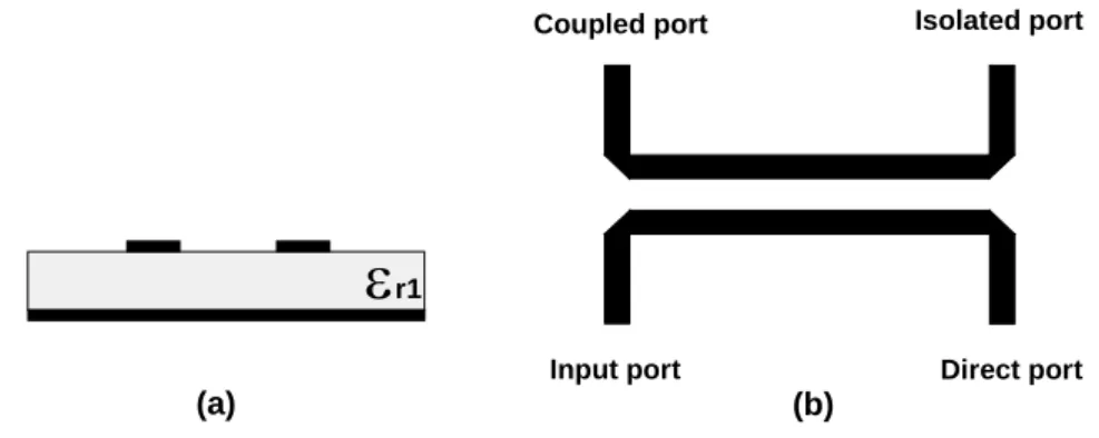
(14) of each proposed configuration is presented in chapter 2. In this chapter, we will summarize various types of existing coupled-line structure, describe research motivation, discuss proposed structures, and give an outline of this dissertation.. 1.1 Coupled Structures When two unshielded transmission lines are placed close to each other, a portion of the power presented on the first line will couple to the second line. The closer the lines are placed, the stronger the coupling takes place. The coupled power on the second line is not only a function of the physical dimensions of the structure but also a function of operation frequency and the propagation mode. Moreover, coupled-line structures can be of any forms and using different types of transmission lines, depending on the demanded application and performance. According to the coupling strength, it can be briefly divided into loosely (<-20dB), moderate (<-8dB), tight (>-3dB), and extremely tight (>-1dB) couplings. Various types of coupling structures with different types of transmissions have different inherent coupling strength which is suitable for different applications of circuits. It is summarized in the following section. In general microwave circuits such as multi-section coupler, and bandpass filters are constructed by various coupled lines with different coupling strength. Also, as the operation bandwidth of coupler becomes wider the coupling strength between different coupled sections will also change accordingly. In some cases, the abrupt change between two sections causes strong discontinuities which should also be considered to achieve wanted circuit performances. Several distinct types of coupled line have been studied. According to the coupling mechanism, they could be categorized in three distinct coupling structures which are edge-coupled, enhanced edge-coupled, and broadside-coupled. These will be discussed in detail in the followings. The most commonly used coupled-line structures is edge-coupled structure as shown in Fig. 1.1 [1] in which the electromagnetic filed interact between coupled lines are only take place on the inner edge of transmission lines. Therefore, the closer of the coupled lines the stronger the coupling strength we can get. Usually, microstrip coupled lines, and microstrip-like lines such as inverted microstrip lines, suspendend microstrip lines, and coplanar waveguide can easily implement these kinds of edge-coupled structures. However, these coupled lines are only suitable for loosely to moderate coupling strength due to practical spacing limitation between two lines in PCB etching process. Edge-coupled structures in microstrip line configuration are planar type, easy to integrate with other circuits, suitable for low cost PCB implementation, and having well developed design formulations. Therefore, it is widely used in many RF and microwave circuits such as loose coupler, narrow band bandpass filters, and DC blocks. However, as the required coupling getting tighter, it becomes 2.
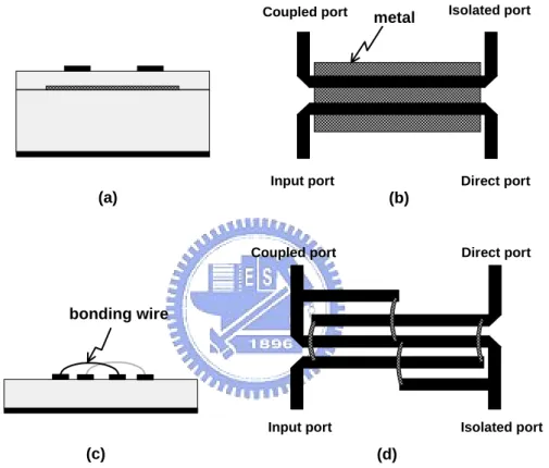
(15) more difficult in practical implementations. Moreover, due to the propagation wave is qusi-TEM mode in microstrip structure, the odd mode phase velocity is faster than the even mode. The unequal modal phase velocity causes poor directivity which degrades some circuit performances. Isolated port. Coupled port. εr1 Input port. (a). Direct port. (b). Fig. 1.1 Edged-coupled microstrip lines (a) cross-sectional view (b) top view.. To overcome the described problems, some coupling structures were proposed which can be categorized as enhanced edge-coupled structures. Fig. 2(a) and (b) show the re-entrant structure [2], Fig. 2(c) and (d) depict the interdigital Lange coupler [3]. Those are two of the most commonly used enhanced edge-coupled structures. Enhanced edge-coupled structures maintain the coupling mechanism of edge-coupled lines and keep the advantages of planar type structure. More importantly, the coupling strength is improved significantly compared to conventional edge-coupled lines. The re-entrant design can largely reduce the odd-mode impedance by introducing the third metal and still keeps the high even-mode impedance. Besides, by properly adjusting the width of the third metal and thickness and dielectric constant of the substrate, the unequal modal phase velocities can be compensated. The Lange coupler combines interdigital arranged strip pairs with air bridges or wire bonding which can increase the odd-mode capacitance. However, these kinds of enhanced edge-coupled structures can realize tight coupling only by use of substrate with related high dielectric constant which is expensive and rarely used in volume production. Further more, extra wire bounding process in the Lange coupler induce parasitic inductance which need tuning back and forth during implementation. Another popular coupled structure usually been adapted to broadband circuit is broadside coupling structures [4]. Fig. 1.3 shows its cross sectional view. In Fig.3, usually three layers of substrates are used. However, if the top layer and bottom layer are air, the structure is so-called suspended substrate broadside coupler. In broadside coupling structure, the odd-mode capacitance involves almost entire overlapping areas. Therefore, increasing the overlapping areas, we can easily achieve a very tight coupling. Unfortunately, the modal phase velocity is usually quite different in suspend substrate broadside coupler. To overcome this, the stripline structure where the three layers of substrate are with the same dielectric 3.
(16) constant is usually adopted. Although broadside coupling in strip line structure can realize an ideal coupler with wide coupling range, these stripline structures usually require special mechanical housing to support it which is complex and need precisely assembly procedures. Moreover, the well known drawback of a conventional stripline is that it is much more difficult to integrate with passive and active components than its microstrip counterpart is. A detail history of research on microwave directional couplers including various types of coupling structures and an extensive reference list is given by Cohn and Levy [5].. Coupled port. Isolated port. metal. Input port. (a). Direct port. (b). Coupled port. Direct port. bonding wire. Input port. (c). Isolated port. (d). Fig. 1.2 Enhanced edge-coupled structures of (a)-(b) re-entrant coupled lines and (c)-(d) Lange coupler.. Air. Air. εr1. εr1 Air. Air. (a). (b). Fig. 1.3 Broadside coupled transmission: (a) Broadside coupled suspended microstrip lines. (b) Offset broadside coupled suspended microstrip lines. 4.
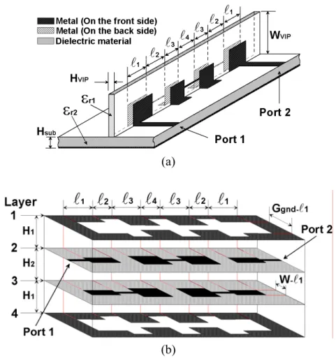
(17) 1.2 Motivation Microstrip lines have been widely used in microwave circuits due to its high level integration of both active and passive components. In several applications such as balanced amplifiers, balanced mixers, etc, a tight coupling of 3dB or more is required. However, the parallel coupled microstrip line is difficult to fulfill the demand of tight coupling strength due to the limitation photo-etching technology. This limitation is also a main challenge to realize a microstrip broadband parallel-coupled filter. The vertically installed planar (VIP) coupled line as shown in Fig. 1.4 was first proposed by Awai [6]. The VIP circuit consists of a broadside coupled line which is vertically soldered with the microstrip line on the main substrate. This VIP coupled line structure can easily achieve a coupling tighter than 3dB. In the mean time, it encounters a serious unequal modal phase velocities. It is the reason why there is no multi-section cascade quadrature hybrid being reported with the conventional VIP coupled lines up to the time of this study. Quadrature hybrid is one of the key elements in many microwave circuits such as balanced amplifier, balanced mixer, phase shifter, power divider, and beam-forming network for array antennas and for direction-finding antennas. Nowadays, ultra-broadband performance with low cost PCB process is demanded in many applications. It is well known that the most common way to realize a 3dB quadrature coupler with multi-octave bandwidth is to cascade of several quarter-wave coupled line sections. However, there are three challenges in practical realization as described in the following. First, the central section of the ultra-broad band multi-section quadrature hybrid (3dB) usually requires an extremely tight coupling (greater than -1dB) and still maintain the same modal phase velocity. For example, in a 5 sections 3 dB quadrature coupler with +/- 0.5dB pass band ripple, the coupling strength in the central section is -0.8dB. From our study, the conventional VIP coupled line structure shown in Fig. 1.4 is difficult to realize such kind of extremely tight coupling (-0.8dB) using low cost PCB substrate material which dielectric constant is usually low (3.3 to 4.4 typically).. WVIP. εr1 HVIP HLz W Hsub. εr2. Fig. 1.4 Cross-sectional view of a conventional VIP coupling structure. 5.
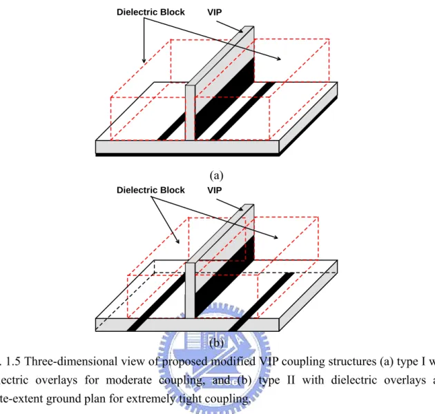
(18) Second, although the unequal phase velocities can be compensated by carefully choosing the vertical substrate [7], it is not suitable for the coupling as tight as -0.8dB. Our investigation shows that the unequal even- and odd-mode modal propagation constants slightly degrade the performances of isolation and return loss of a single section 3dB quadrature coupler. However, the unequal modal phase velocities become a disaster on the performances of a multi-section 3dB quadrature coupler. The degradation of the performances includes the equal-ripple coupling, the isolation, and the return loss over its bandwidth. Hence, the modification on the conventional VIP structure is required to overcome the problem. Finally, when the coupled sections are cascaded, the inner sections of coupled lines always require tighter coupling strength than the outer sections. Therefore, the even- and odd-mode impedances of each section are quite different from those of the adjacent ones. Consequently, the line width of each section abruptly changes at the junction which results in a large discontinuity effect and shows coupling error and directivity degradation. Therefore, to figure out a suitable physical structure of each coupling section that maintains the coupling value but minimizes the discontinuity effect between junctions is very important. In short, the most challenging works to realize a multi-section quadrature hybrid are achieving of an extremely tightly coupled center section, equalizing of modal phase velocities, and minimizing of the discontinuity effect between each section. In the past, only strip line circuits can solve all of these three problems. However, the conventional stripline circuits encounter the drawbacks described previously. In this dissertation two newly proposed VIP coupling structures are presented to realize a microstrip multi-section 3dB quadrature hybrid. The proposed structures are suitable for conventional PCB processes. Shown in Fig. 1.5(a) and (b) are the three-dimensional views of two proposed VIP coupling structures which can achieve the mentioned demands. We call the structure in Fig. 1.5(a) the type I and Fig. 1.5(b) the type II VIP coupling structure. The dielectric blocks at both sides of the VIP coupler, which use similar material as the main and VIP substrate. These dielectric blocks are effective to increase the even-mode effective dielectric constant. As a result, the modal phase velocities could be equalized. In the proposed type I VIP coupling structure, there are four metal strips that two of them are on the VIP substrate and the other two are on the main substrate. The strips on the VIP substrate and the strips on the main substrate are connected at two ends and at the center of the coupler. This structure can implement a coupler with coupling from moderate to tight coupling. The type I VIP coupling structure is impossible to achieve coupling value as tight as -0.8dB even when W equals to 0. To implement the extremely tight-coupled center section for multi-section cascade quadrature hybrid, the type II of modified VIP coupler is proposed as shown in Fig. 5(b). In this Figure, the ground plane in the main substrate changes to two metal strips. Utilizing this finite-extent ground plane (in this case only two ground strips) structure, the VIP coupler can achieve a coupling of tighter than -0.8 dB. Again, a similar dielectric block as the type I is used to compensate the modal phase velocities. 6.
(19) Dielectric Block. VIP. Dielectric Block. VIP. (a). (b) Fig. 1.5 Three-dimensional view of proposed modified VIP coupling structures (a) type I with dielectric overlays for moderate coupling, and (b) type II with dielectric overlays and finite-extent ground plan for extremely tight coupling.. Due to both proposed structures are three-dimensional, various combination of physical dimensions can achieve the same electrical parameters (Z0e, Z0o) for each coupling section. This property provides an extra degree of freedom to overcome the discontinuity effect that occurred at the junctions of two coupling sections. Except the application in the ultra broadband quadrature hybrid, the broadband filter, usually with a bandwidth of broader than an octave, is another attractive application of the extremely tight coupling structure. Many microwave communication systems, for example the UWB system, require very wide bandwidth to handle numerous data simultaneously. Broadband bandpass filters are always on demand for such wideband systems to prevent noise coming into the systems and to minimize spur signals pouring out from defined spectrum. There are many ways to implement broadband bandpass filters. Each kind of broadband bandpass filter has its own advantages and disadvantages. The benefits and drawbacks of each design will be discussed in more detail in chapter 4. Among these filters, the coupled line filter is one of the most popular methods to implement this kind of filters. The coupled line filters such as parallel coupled filters, interdigital filters, and comb-line filters usually 7.
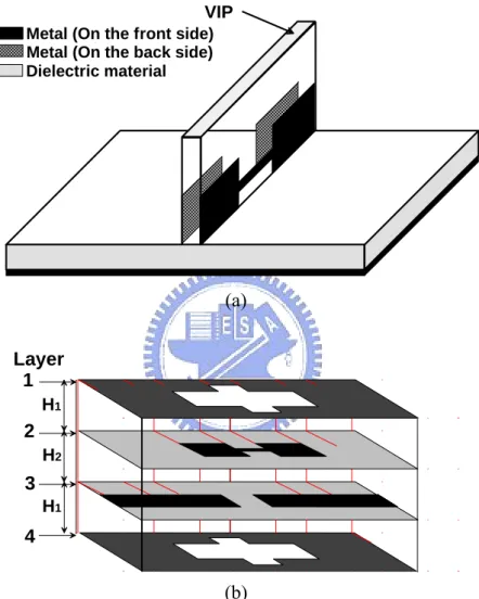
(20) encounter poor upper stopband problem. The stepped impedance resonator (SIR) [8] technique will be adopted in this dissertation to solve the upper stopband problem. However, due to the requirements of large high to low impedance ratio and broad bandwidth of the filter, the extremely tight coupling structures are required. In this dissertation, two newly proposed broadband SIR filter structures as shown in Fig. 1.6(a) and (b) are introduced.. VIP Metal (On the front side) Metal (On the back side) Dielectric material. (a) Layer 1 H1. 2 H2. 3 H1. 4. (b) Fig. 1.6 The proposed filter resonator structures. (a) Structure A use the vertically installed planar stepped impedance resonator (VIPSIR), and (b) structure B adopts the suspended substrate stripline stepped impedance resonator (SSSSIR).. Fig. 1.6(a) shows the structure that we call it structure A. In structure A, the vertically installed planar stepped impedance resonators (VIPSIRs) are adopted. In Fig. 1.6(a), the extremely tightly coupled low impedance line section is a vertically installed planar coupler while the very high impedance uncoupled-line section is also implemented on the vertical substrate. The conventional VIP coupling structure shown in Fig. 1.4 has the advantages of simple physical structure, small size, capable of using normal PCB process, and easy to 8.
(21) achieve tight coupling. However, due to the unequal modal phase velocities, only a few applications such as single section 3dB quadrature coupler [6, 7] and filter [9] have been reported using conventional VIP structure. These two applications are both not sensitive to unequal modal phase velocities. However, the filter structure in [9] using VIP uniform impedance resonator (UIR) is a comb-line-like filter structure. The UIR filter usually has poor upper stopband performance. Besides, the comb-line-like structure in [9] is difficult to realize a filter with the order higher than two due to the complex and strong cross coupling effects between different VIP substrates. The proposed VIPSIR filter solves all of the mentioned problems. Although the VIP structure is a three dimensional structure, it can be assembled by a properly designed soldering fixture. As far as we know, the VIP structure has already been used in many mass-produced commercial PCB circuits as a dual band printed inverted-F antenna. Fig. 1.6(b) depicts the structure B which uses a suspended substrate stripline stepped impedance resonator (SSSSIR). Similar to the structure A, SSSSIR filter also has a tightlycoupled low-impedance coupled-line section and a very high impedance uncoupled-line section. These are implemented in a proposed modified stripline structure where their ground plane has a designed opening. We call it suspended substrate stripline (SSS). For the coupled-line section, both filter structures can realize a very high even-mode impedance (Z0e), and an extremely low odd-mode impedance (Z0o). For the uncoupled-line section, both structures can implement a very high impedance transmission line. Although Fig. 1.6(a) and (b) show a filter with only one resonator, it can be extended to a filter of any order.. 1.3 Chapter Outline. In this section a brief outline of this dissertation will be given as following. Chapter 1 gives a brief introduction which introduces coupler in different aspect. Chapter 2 describes the proposed two modified VIP coupled line which is suitable for multi-octave equal-ripple 3dB quadrature hybrid in detail. In the same chapter, another two structures that are suitable for implementing broadband bandpass filters with wide upper stopband are also presented. In chapter 3, we introduce the design example of multi-octave equal-ripple quadrature hybrid using proposed modified VIP coupled lines. Several design examples of broadband filters with very wide upper stopband clearance using VIPSIRs and SSSSIRs are presented in chapter 4. The finally conclusion are given in chapter 5.. 9.
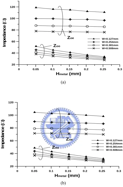
(22) Chapter 2 Analysis and Characteristic of Proposed Structure Practical realization of cascaded multi-section quadrature hybrid with multi-octave bandwidth has three challenges. Those are (1) difficult to implement extremely tight coupling, (2) compensate the un-equal modal phase velocities and (3) overcome the junction effects that occur when cascading several coupled sections. Two proposed modified VIP coupled structures as shown in Fig. 1.5 (a) (b) can solve all three challenges. Detail analysis of each structure is presented in section 2.1. In section 2.2, the analysis and characteristics of VIPSIR and SSSSIR which is suitable for implement a broadband filter are described.. 2.1 Analysis and Characteristic of Proposed Modified VIP Coupled Lines The cross-sectional views of proposed modified VIP coupling structures are shown in Fig. 2.1. In order to compensate the unequal modal phase velocities, which is the most challenging work for implementing a VIP coupler, two dielectric blocks are placed at both sides of the VIP coupler. Due to the odd-mode filed is bounded within the VIP substrate; the odd-mode modal phase velocity is lower than the even mode. By using the dielectric block with similar material as the main and VIP substrate, more even mode field will pass through the dielectric block. Thus, we can slow down the even-mode phase velocity to equalize it with odd-mode phase velocity. In Fig. 2.1(a), there are four metal strips that two of them are on the VIP substrate and the other two are on the main substrate. The strips on the VIP substrate and the strips on the main substrate are connected at two ends and at the center of the coupler. This structure can implement a coupler with coupling from moderate to tight coupling. The even- and odd-mode characteristic impedances with respect to the VIP metal height (Hmetal) 10.
(23) and the width of the strips on the main substrate (W) are extracted by EM simulation tool HFSS. Fig. 2.2(a)-(b) depicts the extracted even- and odd-mode characteristic data of proposed type I structure, in which the gap width between two strips on the main substrate (G) is 0.4572mm (18mils) and 0.7112mm (28mils) respectively. Observing these curves depicted in Fig. 2.2, the even-mode impedance is mainly decided by the width of the strips on the main substrate (W) while the odd-mode characteristic impedance is mostly controlled by the VIP metal height (Hmetal). The gap G provides another degree of freedom to choose the total width of the coupler so that the layout of the junction between adjacent sections could have minimal discontinuity.. (a). (b) Fig. 2.1 Cross-sectional views of (a) type I, and (b) type II of the modified VIP couplers, where Hsub=0.508mm, WVIP=0.2032mm, HVIP=3.048mm, WDR=5.08mm, Wgnd=0.381mm, HDR=1.524mm, and εr1=εr2=εr3=3.38.. 11.
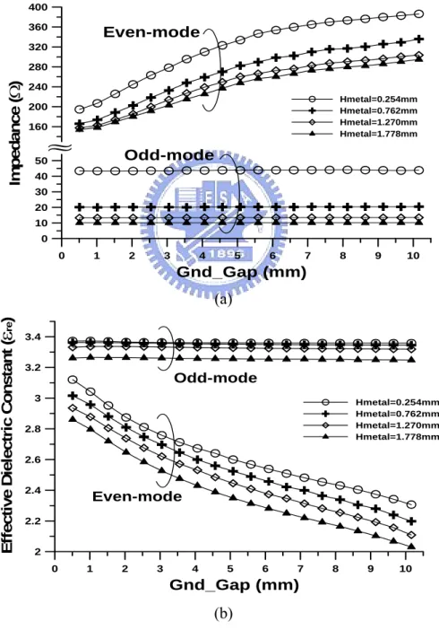
(24) Impedance (Ω). 120. 100. 80. Zoe. W=0.127mm W=0.254mm W=0.381mm W=0.508mm. 60. Zoo 40. 20 0. 0.05. 0.1. 0.15. 0.2. 0.25. 0.3. Hmetal (mm). (a). 120. Impedance (Ω). 100. 80. Zoe. 60. W=0.127mm W=0.254mm W=0.381mm W=0.508mm. Zoo 40. 20 0. 0.05. 0.1. 0.15. 0.2. 0.25. 0.3. Hmetal (mm). (b) Fig. 2.2 Even- and odd-mode characteristic impedances versus VIP metal height (Hmetal) of the type I VIP coupler with (a) G=0.4572mm, and (b) G=0.7112mm.. The type I of modified VIP coupler can not achieve coupling value as tight as -0.8dB even when W equals to 0. To implement the extremely tight-coupled center section, the type II modified VIP coupler is proposed. Fig. 2.1(b) shows the cross-sectional view of type II VIP coupler. In this Figure, the ground plane in the main substrate changes to two metal strips. Utilizing this finite-extent ground plane (in this case only two ground strips) structure, the 12.
(25) VIP coupler can achieve a coupling of tighter than -0.8 dB. Again, two similar dielectric blocks as those of type I structure are used to compensate the modal phase velocities. The even- and odd-mode characteristic impedances versus various VIP metal heights (Hmetal) and ground strip spacing (Ggnd) are shown in Fig. 2.3(a). Similarly, Ggnd and Hmetal separately control the even- and odd-mode characteristic impedances (Z0e, Z0o). Here the width of the ground plan strips (Wgnd) is chosen to be 15 mils for simplifying the design. Depicted in Fig. 2.3(b) are the even- and odd-mode effective dielectric constants versus different Hmetal and Ggnd. With the help of dielectric blocks, the differences between even- and odd-mode effective dielectric constant can be minimized. 400 360. Even-mode. 320. Impedance (Ω). 280 240 Hmetal=0.254mm Hmetal=0.762mm Hmetal=1.270mm Hmetal=1.778mm. 200 160. 50. ∼ ∼. Odd-mode. 40 30 20 10 0 0. 1. 2. 3. 4. 5. 6. 7. 8. 9. 10. Gnd_Gap (mm) Effective Dielectric Constant (εre). (a) 3.4 3.2. Odd-mode. 3. Hmetal=0.254mm Hmetal=0.762mm Hmetal=1.270mm Hmetal=1.778mm. 2.8 2.6 2.4. Even-mode. 2.2 2 0. 1. 2. 3. 4. 5. 6. 7. 8. 9. 10. Gnd_Gap (mm). (b) Fig. 2.3 (a) even- and odd-mode characteristic impedances, and (b) effective dielectric constants versus Ggnd and Hmetal of the type II VIP coupler. 13.
(26) 2.2 Structure of Proposed VIPSIR and SSSSIR The proposed two filter structures are depicted in Fig. 2.4. Fig. 2.4(a) shows the structure A where the vertically installed planar stepped-impedance resonators (VIPSIRs) are adopted. In Fig. 2.4(a), the extremely tightly coupled low impedance line section is a vertically installed planar coupler while the very high impedance uncoupled-line section is also implemented on the vertical substrate. Fig. 2.4(b) depicts the structure B which uses suspended substrate stripline stepped-impedance resonators (SSSSIRs) with a similar tightly-coupled, low-impedance coupled-line section and very high impedance uncoupled-line section. For the coupled-line section, both filter structures can realize a very high even-mode impedance (Z0e), and an extremely low odd-mode impedance (Z0o). For the uncoupled-line section, both structures can implement a very high impedance transmission line. Although Fig. 2.4(a) and (b) show only a three-order filter, it can be extended to a filter of any order.. (a). (b) Fig. 2.4 The proposed filters structures. (a) Structure A where the vertically installed planar stepped impedance resonators are used, and (b) structure B where the modified stripline stepped impedance resonators are used. 14.
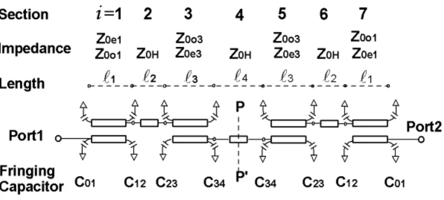
(27) The bandpass filter using VIP structure was first introduced by Zhao and Awai [9] where uniform impedance resonators (UIR) were used. The UIR filter causes a poor upper stopband performance. Besides, the comb-line-like filter structure in [9] is difficult to realize a filter with order higher than two due to difficulties of assembling two closely separated vertical substrates and the strong cross-coupling effects between nonadjacent vertical strips. The proposed structure A uses a single vertical substrate to implement a filter of any order and needs no backside pattern or via holes on the main substrate. Therefore, a PCB with high-density, double-sided components is allowed. Moreover, the conventional low cost, low dielectric constant substrates could be used for both vertical substrate and main substrate. Although the structure A is a three-dimensional structure and is once considered hard to implement, a properly designed soldering fixture can assemble it. The conventional stripline or suspended stripline, which needs a complicated mechanical housing to support, is costly and difficult to assemble. Although, the cross sectional view of the proposed structure B looks somewhat like a suspended stripline structure, the proposed structure B using suspended substrate stripline with ground apertures on top and bottom plans, shows following advantage. In the suspended stripline a precisely fabricated mechanical housing is important because the even-mode impedance of the tight coupled-lines and the impedance values of high impedance lines are very sensitive to the distance between strips and the walls of the metal housing surround them. However, the fabrication and assembly tolerance of such kind of metal housing is large which leads to a poor repeatability. In contrast, the proposed filter structure B requires no metal enclosure and can be easily realized by standard low-cost multi-layer PCB fabrication process which provides almost identical result from board to board. With apertures on the top and bottom ground plane, structure B can realize a coupled line with extremely high even-mode impedance (Z0e) and low odd-mode impedance (Z0o) as well as an uncoupled line with very high impedance.. Fig. 2.5 Equivalent circuit for structure A and B in Fig. 2.4, where P-P’ is the symmetrical plane. 15.
(28) The equivalent circuit of the proposed filter using structure A or B is shown in Fig. 2.5. The circuit parameters in the equivalent circuit will be extracted and be transformed into a series of design charts corresponding to structure A and B, respectively. Therefore, the proposed filters can be designed by a circuit simulator with good accuracy following these design charts without using of time consuming EM simulator. In chapter 4, the proposed design procedures have been examined with several examples where the measured results confirm very well with the simulated ones.. 2.3 Analysis and Characteristic of Proposed Filter Structure 2.3.1 Characteristics of Filter structure A Fig. 2.4(a) illustrates the configuration of proposed filter structure A where a main substrate and a vertical substrate are installed as shown. The stepped impedance resonators (SIRs) are patterned on the front and backside of the vertical substrate in a parallel-coupled manner such that the equivalent circuit in Fig. 2.5 could characterize the filter. In Fig. 2.5, the coupled-line sections represent the vertically installed planar (VIP) coupled lines; the uncoupled transmission lines represent the high impedance lines on the vertical substrate, and the capacitors represent the open-end and step-junction fringing capacitance. Each of them is discussed in detail as following. First, the cross-sectional physical parameters of a VIP coupled line and a high impedance line are shown in Fig. 2.6(a) and (b), respectively. The parameters used in the design charts are similar to Fig. 2.6 unless otherwise specified in each figure. In order to characterize the properties of the coupled-line section of filter structure A, a 3D EM simulator, HFSS, is applied to extract the even- and odd-mode characteristic impedances (Z0e, Z0o) and the corresponding effective dielectric constants (єree, єreo). Fig. 2.7 depicts the modal characteristic impedances versus the strip width (WLZ) on the vertical substrate with various patch widths (W) on the main substrate. The corresponding modal effective dielectric constants (єree, єreo) are shown in Fig. 2.8. The modal characteristic impedances varying with respect to W and WLZ can be summarized as follows. Increasing the patch width (W) on the main substrate would mainly decrease the even-mode impedance and increasing the strip width (WLZ) on the vertical substrate would mainly decrease the odd-mode impedance. The even-mode effective dielectric constant decreases as the patch width (W) and the strip width (WLZ) reduce. On the other hand, the odd-mode effective dielectric constants approach to a constant as increasing the strip width (WLZ). With the help of the design curves in Figs. 2.7 and 2.8, the physical dimensions of a vertically installed planar-coupled line corresponding to a specified Z0e and Z0o could be obtained easily. Second, the high-impedance, uncoupled line on the vertical substrate as shown in Fig. 16.
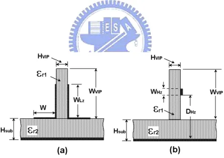
(29) 2.6(b) leads to a high impedance ratio (R=Z0H / Z0L) of a stepped impedance resonator (SIR). Higher impedance of the uncoupled line implies broader upper stopband clearance of the filter structure A. The characteristic of uncoupled line on the vertical substrate is depicted in Fig. 2.9, which shows the characteristic impedances and effective dielectric constants of the high impedance line versus distance (DHZ) between high-impedance line and the main substrate. It is clear that increasing the distance (DHZ) would increase the characteristic impedance of the high impedance line. Although decreasing the metal width (WHZ) of the high impedance line will also slightly affect the line impedance, it is not the main factor to control the line impedance. Therefore, the line width (WHZ) is fixed to be 0.254mm (10mils) in our design in order to tradeoff between higher characteristic impedance and good PCB etching accuracy. Last, the open-end and step-junction fringing capacitance increase according to the strip width (WLZ) on the vertical substrate. The accurate capacitance value can be extracted from EM simulated results. As a result, the capacitance approaches to a limiting value of 0.03pF as the strip width (WLZ) on the vertical substrate greater than 0.762mm (30mils). Fortunately, the strip width (WLZ) on the vertical substrate is always greater than 0.762mm (30mils) in our filter examples so that the fringe capacitance could be set as 0.03pF.. Fig. 2.6 Cross-sectional views of filter structure A. (a) vertically installed planar-coupled line, and (b) high impedance uncoupled line, where Hsub=0.508mm, HVIP=0.2032mm, WHZ=0.254mm, WVIP=3.048mm, and єr1=єr2=3.38 are chosen in this paper.. 17.
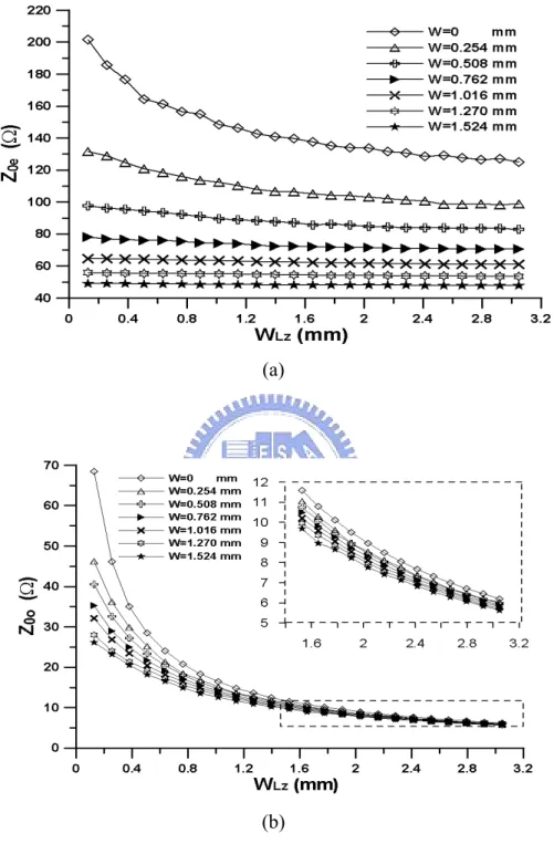
(30) (a). (b). Fig. 2.7 (a) Even-mode and (b) Odd-mode characteristic impedances versus strip width (WLZ) on the vertical substrate with various patch width (W) on the main substrate, where Hsub=0.508mm, HVIP=0.2032mm, WHZ=0.254mm, WVIP=3.048mm, and єr1=єr2=3.38.. 18.
(31) (a). (b). Fig. 2.8 (a) Even-mode and (b) Odd-mode effective dielectric constants versus strip width (WLZ) on the vertical substrate with various patch width (W) on the main substrate, where Hsub=0.508mm, HVIP=0.2032mm, WHZ=0.254mm, WVIP=3.048mm, and єr1=єr2=3.38.. 19.
(32) Fig. 2.9 Effective dielectric constant and characteristic impedance versus the distance (DHZ) between high impedance line and the main substrate where the strip width WHZ on the vertical substrate is fixed to be 0.254mm, Hsub=0.508mm, HVIP=0.2032mm, WVIP=3.048mm, and єr1=єr2=3.38.. 2.3.2 Characteristics of Filter Structure B The proposed filter structure B is realized by the conventional multi-layer PCB fabrication process. There are totally four layers of conductor. The top (first) and bottom (fourth) layers are ground conductors and the second and third layers are the broadside-coupled, stepped impedance resonators. The broadside-coupled lines form the strong coupling sections and high impedance uncoupled lines provide the high impedance ratio of the SIR. Therefore, the same equivalent circuit as shown in Fig. 2.10 could also be applied to the filter structure B. The cross sectional view of broadside-coupled line and the high impedance uncoupled line are depicted in Fig. 2.10(a) and (b), respectively. Structure B has the benefit of easy fabrication. However, comparing to structure A, structure B can not use its aperture region of both upper and bottom side of the substrate to place circuit components. Using the EM simulator, HFSS, the similar design curves of Z0e, Z0o and єree, єreo corresponding to various ground aperture size (Ggnd) and coupled-line widths (W) can be extracted as shown in Fig. 2.11-2.12. Due to the odd-mode EM field being bounded within the coupling strip, the Z0o is mainly controlled by W and is almost independent of the value of 20.
(33) Ggnd. On the other hand, if Ggnd is greater than W, the Z0e increases as the Ggnd increases. These characteristics make it simple to obtain the required values of Z0e/Z0o by only adjusting W and Ggnd. Fig. 2.13 illustrates the effective dielectric constant and characteristic impedance of the high impedance line as a function of ground aperture size (Ggnd). Here, the line width WHZ is fixed to be 0.2032mm (8 mils) in our design in order to tradeoff between higher characteristic impedance and good PCB etching accuracy. The values of fringing capacitors of structure B are larger and more complicated than structure A. Therefore, effort should be paid to extract their values more accurately. The extraction of fringing capacitance values can be done easily by computer optimization where the fringing capacitors correlate the scattering parameters of the circuit model and the results from EM simulation. In our proposed filter structure B, the step-junction capacitance could be considered to be the same as the open-end capacitance due to the large abrupt change on the junction width. The fringing capacitors of each section could be extracted separately, thus, the efforts of EM simulation and circuit extraction could be reduced.. Fig. 2.10 Cross-sectional views of the filter structure B. (a) broadside-coupled line, and (b) high impedance uncoupled line, where H1=0.508mm, H2=0.2032mm, WHZ=0.2032mm, єr1=єr2=3.38, and P-P’ is the symmetrical plane. Due to symmetry only half of the structures are shown.. 21.
(34) (a). (b). Fig. 2.11 (a) Even-mode and (b) Odd-mode characteristic impedances versus ground plane aperture size (Ggnd) with various broadside coupled-line width (W), where H1=0.508mm, H2=0.2032mm, WHZ=0.2032mm, and єr1=єr2=3.38.. 22.
(35) (a). (b). Fig. 2.12 (a) Even-mode and (b) Odd-mode effective dielectric constants versus ground plane aperture size (Ggnd) with various broadside coupled-line widths (W), where H1=0.508mm, H2=0.2032mm, WHZ=0.2032mm, and єr1=єr2=3.38.. 23.
(36) Fig. 2.13 Effective dielectric constant and characteristic impedance of uncoupled line versus the ground plane aperture size (Ggnd), where H1=0.508mm, H2=0.2032mm, WHZ=0.2032mm, and єr1=єr2=3.38.. 24.
(37) Chapter 3 Analysis, Design and Realization of Ultra-Broadband Multi-Section Quadrature Hybrid 3.1 Literature Survey A single-section VIP quadrature hybrid using PCB process has been demonstrated in [6, 7] but none of the multi-section quadrature hybrids using PCB process has been reported. The most difficult issues to realize a multi-section quadrature hybrid are achieving the extremely tight-coupled center section, equalizing the modal phase velocities, and minimizing the discontinuity effect between each section. In the past, only strip line circuit can solve all these three problems. Unfortunately, unlike microstrip circuit, the stripline circuit needs a complex metal housing. For microstrip implementation, Lange [3] coupler using high dielectric constant substrate can achieve tight coupling of about -3dB but it is not suitable for PCB process (due to PCB’s low dielectric constant substrate) and could not achieve required -0.8dB of coupling. Besides, multi-section quadrature hybrid using Lange coupler and parallel-coupled lines encounters serious discontinuity problem at the junction between each section. VIP coupler in [7] solves the problem of PCB realization of tight coupled lines but their modal phase velocities are not compensated. And according to our analysis, the structure in [7] can not realize a coupler with coupling as tight as -0.8dB. Many studies [10-14] have been conducted to compensate the modal phase velocities of a coupler. However, none of them is suitable for VIP coupler. In this chapter, we adopt two modified VIP couplers as discussed in chapter 1 to overcome the realization challenges of a 5-section ultra-broadband quadrature hybrid. The two outer sections use conventional microstrip parallel-coupled lines and the three inner sections comprise two types of modified VIP couplers where one of them provides extra layout flexibility for minimizing the discontinuity between each section. 25.
(38) Moreover, special dielectric blocks are proposed to equalize the modal phase velocities of the proposed modified VIP couplers which have been discussed in chapter 2.. 3.2 Theory and Design Procedures The schematic circuit representation of a single-section coupler is shown in Fig. 3.1 where the port 1 is the input port, port 2 is the through port, port 3 is the coupled port and port 4 is the isolated port. Because the network is symmetrical about the plan P-P’, the even- and odd-mode analysis could be adopted. The 4-ports network shown in Fig. 3.1 could be analyzed easily by decomposed into even- and odd-mode excitation as shown in Fig. 3.2(a) and (b), respectively. In Fig. 3.2(a) and (b), the Z0e and Z0o are the characteristic impedances and θe and θo are the transmission phases of the even and odd mode, respectively.. θe,θo. Z0. 3. 4. Z0e , Z0o. P. Z0. P'. + Z0. 2V -. 2. 1. Z0. Fig. 3.1 Schematic circuit representation of a single-section coupler.. θe. Z0. + V -. Z0e. 3 P. M-wall. 4. Z0. P'. + V -. Z0. Z0e. 1. (a) 26. 2. Z0.
(39) θo. Z0. + V -. Z0o. 3 P. E-wall. 4. Z0. P'. V +. Z0. Z0o. 1. 2. Z0. (b) Fig. 3.2 Schematic circuit expression of coupler with (a) even mode excitation and (b) odd mode excitation.. Using these equivalent circuits, the ABCD matrices of the even- and odd-mode excitation can be expressed as ⎡ Ae ⎢C ⎣ e. Be ⎤ ⎡ cos θ e = De ⎥⎦ ⎢⎣ jY0 e sin θ e. jZ 0 e sin θ e ⎤ cos θ e ⎥⎦. (3.1). Bo ⎤ ⎡ cos θ o = Do ⎥⎦ ⎢⎣ jY0 o sin θ o. jZ 0 o sin θ o ⎤ cos θ o ⎥⎦. (3.2). And ⎡ Ao ⎢C ⎣ o. And, the corresponding even- and odd-mode scattering matrices can be obtained. ⎡S. [ Se ] = ⎢ S11e ⎣. 21e. ⎡S. [ So ] = ⎢ S11o ⎣. 21o. S 21e ⎤ S 22 e ⎥⎦. (3.3). S 21o ⎤ S 22 o ⎥⎦. (3.4). Where,. S11e = S22 e =. S11o = S22 o =. j ( ZZ00e − ZZ00e ) sin θ e. (3.5). 2 cos θ e + j ( ZZ00e + ZZ00e ) sin θ e j ( ZZ00o − ZZ00o ) sin θ o. (3.6). 2 cos θ o + j ( ZZ00o + ZZ00o ) sin θ o. 27.
(40) S 21e = S 21o =. 2 2 cos θ e + j (. Z0 e Z0. 2 cos θ o + j (. Z0 o Z0. (3.7). + ZZ00e ) sin θ e. 2. (3.8). + ZZ00o ) sin θ o. and Z0 is the port impedance of the coupler. Finally, after composition of these modal parameters, the various elements in the 4-port scattering matrix are given as follows:. S11 =. S11e + S11o , S12 = S21 , S13 = S31 , S14 = S41 2. S 21 =. S21e + S21o S + S22 o , S 22 = 22 e , S 23 = S41 2 2. S 24 =. S22 e − S22 o S −S , S31 = 11e 11o , S32 = S41 , S33 = S11 , S34 = S21 2 2. S 41 =. S21e − S21o , S42 = S24 , S 43 = S21 , S 44 = S22 2. (3.9). Following conditions should be satisfied for perfect port match and isolation. S11e = − S11o , S 22 e = − S22 o , and S 21e = S 21o Comparing (3.5) and (3.6), the conditions S11e = − S11o and S22 e = − S22 o are satisfied for arbitrary transmission phase θ (assuming θ=θe=θo) as long as Z0e Z0 = Z 0 Z 0o or. Z 0 e Z 0 o = Z 02. (3.10). The equation (3.10) is also satisfied the condition ( S 21e = S 21o ) under the condition θ=θe=θo. Therefore, (3.10) gives the necessary condition for TEM backward-wave directional coupler. When the propagation wave is non TEM wave (θe≠θo), only Z0e=Z0o can satisfied the matching condition at all ports. However, there is no meaning for a coupler to set Z0e=Z0o. In other words, theoretically, only TEM mode propagation structure can realize a matched coupler. However, in practical application for a single-section coupler even the phase different between even- and odd-mode is over 30% the return loss is still in acceptable value of 15dB. From (3.9) and (3.10) assuming (θ=θe=θo), we obtain Z0 S 21 = (3.11) 2 Z 0 cos θ + j ( Z 0 e + Z 0 o ) sin θ ( Z 0e − Z 0o ) S31 = (3.12) ( Z 0 e + Z 0 o ) − j 2 Z 0 e Z 0 o cot θ 28.
(41) From equation (3.11) and (3.12) we know that the coupling (S31) and the through (S21) of the coupler are both a function of θ. And when the θ = π2 , the coupling could be simplified as. K=. Z0e − Z0o Z0e + Z0o. (3.13). In equation (3.13) K is called the coupling factor which defines as the coupling at the central frequency of a coupler. Therefore, the maximal coupling between port 1 and 3 (or port 2 and 4) occurs when θ = π2 and the maximal coupling values are given by S31 = S13 = S 24 = S 42 = K. Further, when θ = π2. S21 = S12 = S34 = S 43 = 1 − K. Thus, the scattering matrix of a backward-wave coupler with quarter-wave length can be represented as follows:. ⎡ ⎢ ⎢− j [S ] = ⎢ ⎢ ⎢ ⎢⎣. − j 1− K 2. K. 1− K 2. 0. 0. K. 0. 0. 0. K. − j 1− K 2. 0. ⎤ ⎥ ⎥ K ⎥ 2 − j 1− K ⎥ ⎥ ⎥⎦ 0 0. (3.14). Although the above described theory is only valid for a single-section direction coupler, it is the basic building block of a multi-section directional coupler. Each section of multi-section directional coupler is a single-section direction coupler with designed coupling factor so that a good single-section directional coupler is the most important part to build a multi-section directional coupler.. Fig. 3.3 A N-section cascaded symmetrical quadrature hybrid.. 29.
(42) In order to obtain a near-constant coupling over a wider frequency range, a multi-section coupler structure is the most commonly used method. The multi-section coupler cascades several sections of coupler with various coupling factors. Each section is quarter wave length long at center frequency. By properly choosing the even- and odd-mode impedances of each section, the multi-section coupler could have a Chebyshev or Butterworth type of response over a broad bandwidth. The multi-section coupler could be either symmetrical or asymmetrical. Shown in Fig. 3.3 is a symmetrical multi-section coupler. For a 900 quadrature coupler, the circuit should be symmetric. An N-section directional coupler contains N different single-section coupler in a cascaded manner. Each single section is denoted by the even- and odd-mode characteristic impedances. As shown in Fig.2.2b, the i-th section in symmetrical coupler will be identical to the (N+1-i)th section. The signal goes out from the through port is 900 out of phase to that of the coupled port (∠S31=∠S21+90 degree). This phase relationship is independent of frequency. Because of this property, the 3-dB symmetrical directional couplers are widely used in several microwave circuits such balanced amplifier, balanced mixer, phase shifter, power divider, and beam-forming network for array antennas and for direction-finding antennas. The asymmetrical multi-section coupler does not have the mentioned phase property as symmetrical one and is not as popular as symmetrical multi-section coupler. Here, only the symmetrical multi-section coupler will be discussed. An analytical design expression of a multi-section directional coupler is very cumbersome even the order is small. However, synthesis of multi-section symmetrical TEM coupler using insertion loss method has been presented by Cristal and Young [15]. Moreover, the design tables for equal-ripple and maximally flat responses of multi-section symmetrical coupler up to nine sections are generated in [15]. Therefore, the design procedures of multi-section cascaded coupler are described as follow. 1). 2). 3) 4). According to the specification for desired coupler, utilize the design table to obtain the required number of sections and the even- and odd-mode characteristic impedances of each section. Here, a 5-section symmetrical 3dB quadrature hybrid is chosen as an example. Usually, the outmost sections (section 1 and 5) are the most loosely coupled sections. The conventional parallel-coupled microstrip lines are suitable for these sections. For this kind of coupled lines, commercial circuit simulators such as ADS, or Microwave Office can get the physical dimensions easily. Use Fig. 2.3 (a) and (b) to obtain the physical dimensions of the central section (section 3) which is the most critical one. Last, to design the inner sections (section 2 and 4), designers should properly choose the width and distance of the strips on the main substrate by the aid of Fig. 2.2 (a) and (b) to minimize the discontinuities between sections (especially between the outmost sections). 30.
(43) 5). Finally, the whole multi-section quadrature hybrid performances are verified by 3-D EM simulator HFSS.. 3.3 Ultra-Broadband Multi-Section Quadrature Hybrid Using Modified VIP Coupler In this section, a quadratrue hybrid with a passband ripple of +/- 0.5dB and frequency range of 1-9GHz is demonstrated. According to the design table listed in [9], five sections are needed to fulfill such specifications and the corresponding even- and odd-mode characteristic impedances of each section are detailed in table 3.1.. Table 3.1 Design parameters and physical dimensions of experimental coupler Coupler Specifications Freq 1-9GHz. C (dB) 3dB. Ripple +/-0.5dB. Dimension (mm) Section Z0e. Z0o. W. G Hmetal Ggnd. L. I=1,5 58.8 42.5. 1.1 0.38 NA. NA. 9.0. I=2,4 78.5 31.8. 0.4. 0.6 0.16. NA. 8.0. 233 10.7 NA NA 1.5. 6.6. 8.5. I=3. Based on the above design procedures, the proposed 5-section hybrid is fabricated. The detail physical dimensions of each section are also shown in Table 3.1. The photograph of the proposed 5-section hybrid is shown in Fig. 3.4. The main substrate, VIP substrate and dielectric blocks are all Rogers RO4003 with dielectric constant of 3.38 and thickness of 0.508mm (20mils), 0.2032mm (8mils) and 1.524mm (60 mils) respectively.. Fig. 3.4 Photograph of the fabricated five-section 3dB directional coupler. 31.
(44) Depicted in Fig. 3.5 and 3.6 are the simulated and the measured results that a perfect match could be observed. The simulated and measured amplitude and phase errors are shown in Fig. 3.7. The measured amplitude and phase balances between port 2 (coupled port) and port 3 (through port) are described as following. The amplitude imbalance is less than +/-0.65dB and phase difference is keeping within 900 +/-50 over the designed frequency of 1-9GHz.. Fig. 3.5 Simulated responses of the proposed hybrid.. Fig. 3.6 Measured responses of the proposed hybrid. 32.
(45) Fig. 3.7 Measured and simulate amplitude and phase errors of the proposed hybrid.. 33.
(46) Chapter 4 Analysis, Design and Realization of Broadband Bandpass Filters with Wide Upper Stopband Using Parallel-Coupled VIPSIRs and SSSSIRs 4.1 Literature Survey High performance wideband RF/microwave bandpass filters which need both broad passband and wide upper stopband are highly desirable for next generation broadband wireless communication systems. In the mean time, the conventional multi-layer printed circuit board (PCB) filter which uses low-cost FR4 or PTFE substrate (dielectric constant usually lower than 4.47) with a standard PCB process and requires no metal enclosure is also essential for cost reduction and mass productivity. Considering the low cost PCB filters, although excellent performance has been achieved in conventional RF/microwave filters [1] such as parallel-coupled-line filters, interdigital filters, and comb-line filters, their fractional bandwidth can hardly exceed 50% due to the limitation on realizing tightly coupled lines especially the first and last coupling stages of the broadband filters. Recently, several works have solved the challenge of achieving wide bandwidth with several distinctive approaches such as a dual-mode ring resonator with tuning stubs [16-18], adding a third line in the parallel coupled line to obtain the tight coupling [19], distributed highpass filters with shunt short-circuit stubs [20], cascaded broadside-coupled structure [21], cascade or composite of low pass filters and highpass filters [22-25], and adoption of a multiple-mode resonator [26-29]. Most of the mentioned works can achieve a 34.
(47) filter with bandwidth more than an octave and some of them can be implemented by conventional PCB. However, none of them deal with the presence of spurious passbands which normally occur at 2f0, 3f0 or even 4f0. The presence of these spurious passbands causes poor upper stopband clearance or poor selectivity performance. A well-known method to eliminate the spurious passband is to compensate the modal phase constant near the spurious passband frequency. Many published works based on this theory have been carried out by meandering the coupled line [30], adding compensation capacitors [31-32], and applying wiggly-coupled structures [33]. However, compensation of the modal phase constant over a wide frequency range is so difficult that only a specific harmonic passband, 2f0 for example, can be eliminated [30-32] or it is only valid for narrow band filter [33]. Another spurious passband eliminating method to use transmission zeros at spurious passband frequencies is also effective for narrowband filters but not for broadband filters. Because the spurious passband of a broadband filter is also wideband, a notch-like transmission zero can not suppress such a wideband spurious response. Broadband bandpass filters can also be designed using S-plane highpass or bandpass prototype under Richards transformation [34, 35]. In [34], applying the S-plan highpass prototype can implement a bandpass filter with very broad passband but its upper stopband is not separately controlled. In [35], two broadband bandpass filters with wide stopband clearance have been derived from S-plane bandpass prototypes with specific transmission zero locations using Richards transformation. The implementation of these filters is costly and the assembling process is complicated because a precisely fabricated mechanical enclosure to support the stripline is essential and an extra bounding equipment to construct the series lump capacitors is demanded. As the filter bandwidth gets wider, the spurious passband becomes wide accordingly such that the space of the upper stopband is then squeezed. Therefore, pushing the spurious passband as far as possible from the main passband is essential especially for a broadband filter. A stepped impedance resonator (SIR) [8] has the property of moving the first spurious resonance away from twice of the fundamental resonant frequency. Several researches [36-38] have demonstrated very good performance of stopband clearance by pushing the spurious passband away from main passband. However, none of the proposed structures are applicable to a broadband filter due to their weak coupling strength. In order to push the first spurious resonance as far as possible, the impedance ratio R (R=Z0H/Z0L) of a stepped impedance resonator should be as high as possible where Z0H and Z0L are the characteristic impedance of high impedance and low impedance line sections, respectively. As the impedance ratio increases, the resonator length decreases. As a result, to achieve enough coupling for a broadband filter becomes more difficult. Therefore, special structures should be developed to solve mentioned problems. To the best of the author’s knowledge, no published works have been reported to realize a broadband filter using stepped impedance resonator with very high impedance ratio. 35.
數據
+7
相關文件
According to the regulations, the employer needs to provide either a mobile or landline phone number at which the employer (or a contact person) can be reached.. If
在撰寫網頁應用程式 HTML 的語法當中,以下何者錯誤?(A)<a>是用來製作超連結的標記(Tag) (B)HREF 是一個在<a>與</a>中指定其他
接收器: 目前敲擊回音法所採用的接收 器為一種寬頻的位移接收器 其與物體表
another direction of world volume appears and resulting theory becomes (1+5)D Moreover, in this case, we can read the string coupling from the gauge field and this enables us to
An adaptation layer is used to support specific primitives as required by a particular signaling application. The standard SS7 applications (e.g., ISUP) do not realize that
After the graph is constructed, we can realize that for all
Finally, making the equivalent circuits and filter prototypes matched, six step impedance filters could be designed, and simulated each filter with Series IV and Sonnet program
This thesis studies how to improve the alignment accuracy between LD and ball lens, in order to improve the coupling efficiency of a TOSA device.. We use
