3 4 5 6 7 8 9 10 11
Low Band
3 4 5 6 7 8 9 10 11
High Band
GHz GHz
A CMOS Current Reused Low-Noise Amplifier
for Ultra-Wideband Wireless Receiver
Zhe-Yang Huang1, Che-Cheng Huang2, Yeh-Tai Hung3 and Meng-Ping Chen4
1 Institute of Communication Engineering, National Chiao Tung University, Hsin-Chu, Taiwan 2 NOVATEK, Hsin-Chu, Taiwan
3 Dept. of Electrical and Control Engineering, National Chiao Tung University, Hsin-Chu, Taiwan 4 Institute of Electronics Engineering, National Tsing Hua University, Hsin-Chu, Taiwan
Abstract - A current reused low-noise amplifier (LNA) with gain compensated to extend the bandwidth which is designed for ultra-wideband (UWB) wireless receiver. The design consists of two cascode common-source amplifier and an output buffer which is implemented in 0.18um RF CMOS process. The LNA gives 13.1dB gain; 9.1GHz 3dB bandwidth (3.1-12.2GHz) while consuming 13.9mW through a 1.8V supply. Over the 3.1GHz - 10.6GHz frequency band, a minimum noise figure of 2.7dB and input return loss lower than -8.7dB have been achieved.
Index Term – RFIC, Ultra-Wideband, UWB, Gain Compensated, Current Reused, LNA and Low-Noise Amplifier.
I. INTRODUCTION
Since the approval of the ultra-wideband (UWB) radio technology for low power wireless communication application in February, 2002, [1] UWB systems has become an increasingly popular technology which is capable of transmitting data over a wide spectrum of frequency with very low power and high data rate. Although the IEEE UWB standard (IEEE 802.15.3a [2]) has not been completely defined, two major proposed solutions, MB-OFDM and DS-UWB, are all allowed to transmit in a band between 3.1GHz-10.6GHz and 3.1GHz-9.6GHz. The band definition of MB-OFDM is illustrated in Fig.1 (a) which extended from 3176MHz to 10552MHz and the band definition of DS-UWB are from 3100MHz to 4900MHz and 6000MHz to 9700MHz. The bandwidth of MB-OFDM is containing 1, Group-3, Group-4 and Group-5. Group-2 is not considered in current UWB system which caused by the U-NII band and WLAN (IEEE 802.11a). The bandwidth of DS-UWB is with Low-Band and High-Band which is in Fig.1 (b).
Fig.1 (a) Band Groups of MB-OFDM
Fig.1 (b) Low Band and High Band of DS-UWB
In RF wireless receiver, LNA is one of the most critical building blocks caused by the noise figure is dominated in 1st stage of the receiver that is illustrated in Fig. 2. For
LNA design, there are many trade-off between different specifications. For example, the power gain affects noise figure, the die area affect cost, and the power consumption affects the battery life. This paper is focused on the design and implementation of the UWB specifications; the low–noise amplifier for ultra-wideband receiver is implemented in a 0.18um Standard RF CMOS Process. PA LNA M ixer M ixer PLL DAC ADC DSP
Fig.2 UWB Transceiver Architecture of MB-OFDM
II. DESIGN OF ULTRA-WIDEBAND LNA
A. Wideband Amplifier Design
A simple figure of the wideband amplifier which contains input matching network, main amplifier and output buffer and that is shown as Figure 3. The specification of ultra-wideband system is defined as 3.1GHz-10.6GHz, therefore a very wide bandwidth input matching network is necessary in the UWB LNA. For measurement consideration, the output impedance is always designed for 50 ohms in the output buffer. The design considerations of low-noise amplifier are mainly in input return loss, power gain, and noise figure (NF), linearity (P1dB, IIP3) and power consumption, but there are some trade-off between these important characteristics. 1 Buffer Matching Network RF_IN RF_OUT Av1 Av2
Fig.3 Wideband Amplifier Design
B. Wideband Input Impedance Matching
Wideband input impedance matching is a critical design challenge in ultra-wideband system. Some excellent wideband input impedance matching solutions are proposed in [3]. The wideband input impedance matching network including the conventional source-degeneration input matching and an inductor shunted in input RF path which is shown in Fig. 4; both of the circuits contribute one resonated frequency fr1 and fr2 to
extend the bandwidth of the input matching. Equation (1) is the total equivalent input impedance Zin, where Lg, Ls, Lm are gate inductor, source inductor and matching inductor, Cgs1 is the parasitic capacitor in MOS transistor and ω is the unity gain frequency of the transistor. T
RF_IN M1 Ls Lg Lm Cdc VBias Zin
Fig. 4 Input Impedance Matching Network
2 1 1 2 1
(
1 1) 1
m g gs T m s gs m in g gs T s gs m gss L L C
s L L C
L
Z
s L C
s
L C
L C
ω
ω
+
+
=
+
+
+
(1)C. Cascoded Amplifier with LC-Tank Load
The most popular topology of low-noise amplifier is cascode amplifier with LC tank, as illustrated in Fig. 5(a), which eliminates the Miller effect on input transistor to achieve high-frequency performance. The load with LC-tank is mostly used in narrow-band systems due to its excellent frequency-selective characteristics that are shown as Figure 5(b). And the voltage gain AL1 of this low-noise amplifier is expressed in equation (1), where gm1 is the transconductance of the MOSFET, ro1, ro2 are the output impedance of the transistors, and inductor L, capacitor C are the load of the LC-tank.
RF_IN L C RF_OUT Mn1 Mn2 (a) (b)
Fig. 5 Cascode LNA with LC-tank (a) and Power Gain (b)
2 1 2 L1 1 2 2 1 2 2 1 2
A
m o o m m o o m o osg r r L
g
s g r r LC sL g r r
≈ −
⋅
+
+
(2)D. Cascade Amplifier with LC-Tank Load
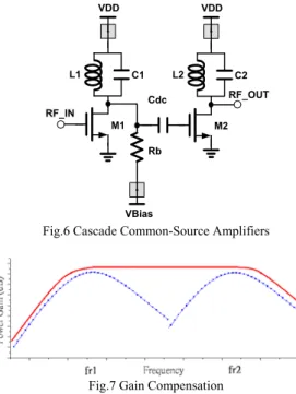
Therefore, two stages of LC-tank resonated amplifiers could achieve higher power gain and wider bandwidth; as shown in Fig.6. The first stage amplifier with LC-tank resonated loading is providing the power gain of lower frequency, and the second stage amplifier is providing the power gain of the higher frequency, which are the blue dash lines in Fig. 7; the resonated center frequency are fr1 and fr2. And final power gain of
the low-noise amplifier is the red solid line in Fig. 7 which is the result of two stage amplifiers in gain compensated; the wide bandwidth is produced.
M1 Rb VBias VDD M2 VDD L1 C1 L2 C2 Cdc RF_IN RF_OUT
Fig.6 Cascade Common-Source Amplifiers
Fig.7 Gain Compensation
E. Proposed UWB Low-Noise Amplifier
The proposed UWB low-noise amplifier is shown in figure 8 which consists of the input matching network that is implemented by the Butterworth Filter [3] where are Lm, Lg, LS and Cgs1; the main amplifier is containing
M1, M2, L1, and L2; the output buffer is the M3; the Cdc
are DC blocking capacitors and Cac is AC ground capacitor. The first stage amplifier M1 contributes the
lower frequency power gain; the RF signal ends at Cac
capacitor, but also travels to Cdc path. Then the second
stage amplifier M2 contributes the higher frequency
power gain. The DC current flows through transistors M1
and M2; therefore, the DC current is saved and the power
dissipation is also saved. The inductor Lsp is a series
peaking inductor, and the power gain in frequency response is extended which is shown in Fig.9; the input return loss is also influenced by this series peaking inductor which dues to the bad isolation of the common-source amplifier that is also shown in Fig. 10. The inductor also reduces the gate noise in higher frequency from the MOSFET M2; the comparison is also available
RF_IN Idc RF_OUT M1 M3 Ls Lg Lm Cdc Cdc VDD VBias VDD VDD M2 L1 Cac Cdc Lsp L2
Fig. 8 Proposed UWB Low-Noise Amplifier
Fig. 9 Power Gain w/o and w/i Series Peaking
Fig. 10 Input Return Loss w/o and w/i Series Peaking
Fig. 11 Noise Figure w/o and w/i Series Peaking
III. SIMULATION RESULTS
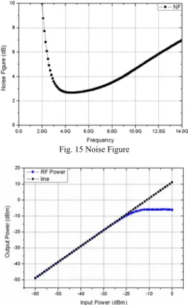
The simulation results of the proposed UWB LNA using Agilent ADS 2006A simulator are given in Figure 12 to Figure 17. In Figure 12 that can be seen the input return loss (S11) are lower than -8.7dB between 3.1GHz to 10.6GHz. In Figure 12, that can be seen that the output return loss (S22) are lower than -10.9dB between 3.1GHz to 10.6GHz, respectively. The power gain whose peak value is 13.1dB at 9.5GHz and which is shown in Figure 14. In Fig. 15, it can be seen that the noise figure is below 4.9dB between 3.1GHz to 10.6GHz and the minimum noise figure are 2.7dB at 4.3GHz through 1.8V supply voltage. The input-referred 1dB compression point (IP1dB) is -19dBm at 7.0GHz which is in Fig. 16. In figure 17, the Third-Order Input Intercept Point (IIP3) at 6336MHz and 6346MHz is -9dBm. The power consumption is 13.9mW through 1.8V supply voltage which neglects the power of output buffer.
Fig. 12 Input Return Loss (S11)
Fig. 13 Output Return Loss (S22)
Fig. 15 Noise Figure
Fig. 16 Input-Referred 1dB Compression Point (P1dB)
Fig. 17 Third-Order Input Intercept Point (IIP3)
IV. CONCLUSIONS
A CMOS UWB LNA is designed with current reused technic for ultra-wideband wireless system; the bandwidth extended from 3.1GHz to 10.6GHz. The simulation results show that the proposed LNA gives 13.1dB power gain for 3.1-10.6GHz, 9.1GHz 3dB bandwidth (3.1-12.2GHz) while consuming 13.9mW through 1.8V power supply.Over the 3.1GHz - 10.6GHz frequency band, a minimum noise figure of 2.7dB have been achieved.
Table.1 Performance Conclusions S11 (dB) < -8.7 S22 (dB) < -10.9 S21 (dB) 10.0 ~ 13.1 S21 Max. (dB) 13.1 Working Bandwidth (GHz) 3.1 ~ 10.6 3dB Bandwidth (GHz) 3.1 ~ 12.2 NF (dB) 2.7 ~ 4.9 NFmin (dB) 2.7 IP1dB (dBm) -19 IIP3 (dBm) [10MHz] -9 Power Consumption (mW) 13.9 ACKNOWLEDGMENT
The authors would like to thank the chip implementation center (CIC) for technical support.
REFERENCES
[1] FCC, "Final Rule of the Federal Communications Commission, 47 CFR Part 15,Sec. 503", Federal Register, vol. 67,no. 95,May 2002.
[2] http://www.ieee802.org/15/pub/TG3a.html
[3] Andrea Bevilacqua, and Ali M. Niknejad, "An Ultrawideband CMOS Low-Noise Amplifier for 3.1-10.6-GHz Wireless Receivers",IEEE JOURNAL OF SOLID-STATE CIRCUITS, Vol. 39, No. 12, pp.2259-2268, Dec 2004.
[4] Chang-Wan Kim, Min-Suk Kang, Phan Tuan Anh, Hoon-Tae Kim, and Sang-Gug Lee, "An Ultra-Wideband CMOS Low Noise Amplifier for 3-5GHz UWB System", IEEE JOURNAL OF
SOLID-STATE CIRCUITS, Vol. 40, No. 2,pp.544-547, Feb. 2005.
[5] Chang, C.-P.; Chuang, H.-R., "0.18 um 3-6 GHz CMOS broadband LNA for UWB radio", Electronics Letters, Volume 41, Issue 12, June 2005 Page(s):33 - 34.
[6] Chih-Fan Liao; Shen-Iuan Liu, "A broadband noise-canceling CMOS LNA for 3.1-10.6-GHz UWB receiver", Custom Integrated
Circuits Conference, 2005. Proceedings of the IEEE 2005, 18-21
Sept. 2005 Page(s):161 - 164.
[7] Zhe-Yang Huang, Che-Cheng Huang, Chun-Chieh Chen and Chung-Chih Hung, “1V CMOS Low-Noise Amplifier with Inductive Resonated for 3.1-10.6GHz UWB Wireless Receiver”,
Proceedings of 2007 IEEE International SOC Conference,
pp.15-18.
Table.2 Comparison of the Proposed UWB LNA with Other Reported Wideband LNA
Paper Circuit Topology Technology S11(dB) S22(dB) S21(dB) BW(GHz) Gmax(dB) NF(dB) NFmin(dB) Pdiss(mW)
[4] resistive feedback 0.18um CMOS < -9 < -10 6.8-9.8 2.0-4.6 9.8 2.3-5.2 2.3 12.6
[5] 3-stages comm.-source 0.18um CMOS <-12.2 < -10.1 13.5-15.8 3.0-6.0 15.76 4.7-6.7 4.7 59.4
[6] 3-stages shunt-peaked 0.18um CMOS < -7 < -12 6.7-9.7 1.2-11.9 9.7 4.5-5.1 4.5 20.0
[7] 2-stages comm.-source 0.18um CMOS < -8.7 < -9.2 9.0-12.0 3.0-11.0 12.0 4.2-7.6 4.2 7.3 This Work Current reused 0.18um CMOS < -8.7 < -10.9 10.0-13.1 3.1-12.2 13.1 2.7-4.9 2.7 13.9