Dark current and trailing-edge suppression in ultrafast photoconductive switches and
terahertz spiral antennas fabricated on multienergy arsenic-ion-implanted GaAs
Tze-An Liu, Gong-Ru Lin, Yen-Chi Lee, Shing-Chung Wang, Masahiko Tani, Hsiao-Hua Wu, and Ci-Ling Pan
Citation: Journal of Applied Physics 98, 013711 (2005); doi: 10.1063/1.1953867 View online: http://dx.doi.org/10.1063/1.1953867
View Table of Contents: http://scitation.aip.org/content/aip/journal/jap/98/1?ver=pdfcov Published by the AIP Publishing
Articles you may be interested in
Terahertz photomixing in high energy oxygen- and nitrogen-ion-implanted GaAs Appl. Phys. Lett. 91, 031107 (2007); 10.1063/1.2753738
Terahertz emission properties of arsenic and oxygen ion-implanted GaAs based photoconductive pulsed sources J. Vac. Sci. Technol. A 24, 774 (2006); 10.1116/1.2183284
Generation of continuous-wave terahertz radiation using a two-mode titanium sapphire laser containing an intracavity Fabry–Perot etalon
J. Appl. Phys. 97, 103108 (2005); 10.1063/1.1904724
Fe-implanted InGaAs photoconductive terahertz detectors triggered by 1.56 m femtosecond optical pulses Appl. Phys. Lett. 86, 163504 (2005); 10.1063/1.1901817
THz radiation emission properties of multienergy arsenic-ion-implanted GaAs and semi-insulating GaAs based photoconductive antennas
J. Appl. Phys. 93, 2996 (2003); 10.1063/1.1541105
Dark current and trailing-edge suppression in ultrafast photoconductive
switches and terahertz spiral antennas fabricated on multienergy
arsenic-ion-implanted GaAs
Tze-An Liu, Gong-Ru Lin,a兲Yen-Chi Lee, and Shing-Chung Wang
Department of Photonics and Institute of Electro-Optical Engineering, National Chiao Tung University, 1001 Ta Hsueh Road, Hsinchu 30010, Taiwan, Republic of China
Masahiko Tani
Institute of Laser Engineering, Osaka University, 2-1 Yamadaoka, Suita, Osaka 565-0871, Japan
Hsiao-Hua Wu
Department of Physics, Tunghai University, Taichung, Taiwan 407, Republic of China
Ci-Ling Panb兲
Department of Photonics and Institute of Electro-Optical Engineering, National Chiao Tung University, 1001 Ta Hsueh Road, Hsinchu 30010, Taiwan, Republic of China
共Received 17 November 2004; accepted 20 May 2005; published online 13 July 2005兲
We report ultrafast共⬃2.7 ps, instrument limited兲 switching responses of a multienergy-implanted GaAs: As+ photoconductive switches 共PCSs兲 with suppressed trailing edge and reduced dark
current. This material is highly resistive with dark current as low as 0.94A at a bias of 40 V. The carrier mobility of the former is⬃590 cm2/ V s, resulting in a small-signal optical responsivity of
⬃2 mA/W. Pumped at 100 mW and biased at 80 V, the multienergy-implanted GaAs:As+ PCS
exhibits peak response共0.35 V兲 comparable to the best result of single-energy-implanted ones. The improvement on photoconductive response is crucial for the generation of shorter terahertz emission pulses from spiral antennas fabricated on multienergy-implanted GaAs: As+ 共0.8 ps兲 than
single-energy-implanted GaAs 共1.2 ps兲, with the central frequency blueshifted to 0.2 THz 共from 0.15 THz兲 and the spectral bandwidth broadened to 0.18 THz 共from 0.11 THz兲. © 2005 American
Institute of Physics.关DOI: 10.1063/1.1953867兴
I. INTRODUCTION
Photoconductive switches共PCSs兲 with ultrashort photo-excited carrier lifetime, good optical responsivity, high breakdown field, and low dark current are essential for fab-rication of optically triggered terahertz antennas.1,2To meet these demands, various classes of carrier-lifetime-shortened semiconductors synthesized by impurity doping, radiation damage, chemical-vapor deposition, and molecular-beam epitaxy 共MBE兲 have been explored. In particular, a nonsto-ichiometric GaAs film grown by MBE at low substrate tem-peratures共referred here after as LT-GaAs兲 with subpicosec-ond carrier lifetime was extensively used.3,4 The absolute epitaxial growth temperature as well as the properties of LT-GaAs, however, is difficult to control due partly to lack of a reliable temperature monitoring instrument at such a low temperature 共⬃200 °C兲 in high vacuum. As a result, the characteristics of LT-GaAs layers could vary even though the other growth parameters remain unchanged. Ion implantation has recently emerged as the most cost-effective method for preparation of substrate material for ultrafast PCS.5 Carrier lifetimes as short as 0.2 ps have been reported for proton-bombarded GaAs, oxygen-implanted silicon on sapphire, and arsenic-ion-implanted GaAs 共GaAs:As+兲.6,7
GaAs: As+,
which exhibits structural properties almost identical to
LT-GaAs, exhibits a precisely and reproducibly controlled ar-senic excess density in the implantation layer. After appro-priate annealing, the highly resistive electrical and ultrafast optoelectronic properties of both GaAs: As+ and LT-GaAs
have made them the best candidates for PCS fabrication. The subpicosecond carrier lifetimes and picosecond photocon-ductive responses of GaAs: As+ and LT-GaAs PCS were comparable.8–10 Recently, the GaAs: As+ has also been
em-ployed to fabricate optically controlled antennas for terahertz-wave generation and reception.11,12 However, the reduction of the persistent falling-tail response and the satu-rating response at high biased voltages of the PCS made on either LT-GaAs or GaAs: As+substrate is still the important
issues to be solved. The long photoexcited carrier decay in these materials can be entirely eliminated using either buff-ered layer epitaxy or high ion-dose implantation.13 On the other hand, we expect that a more uniform implantation pro-file in the PCS through a multienergy or multidosage recipe would also be helpful in suppression of the trailing edge of the terahertz pulse shape and enable a faster emission re-sponse of the GaAs: As+PCS-based terahertz antenna. Other
potential advantages include the improved breakdown char-acteristics of GaAs: As+, which could result in higher
emis-sion efficiency of the antenna under a larger bias field.10 In this work, we report on trailing-edge suppression and dark-current reduction properties of a multienergy-implanted and furnace-annealed GaAs: As+PCS and terahertz antenna. The a兲Electronic mail: [email protected]
b兲Electronic mail: [email protected]
0021-8979/2005/98共1兲/013711/4/$22.50 98, 013711-1 © 2005 American Institute of Physics [This article is copyrighted as indicated in the article. Reuse of AIP content is subject to the terms at: http://scitation.aip.org/termsconditions. Downloaded to ] IP:
improvement on photoconductive response is crucial for the generation of shorter terahertz emission pulses from spiral antennas fabricated on multienergy-implanted GaAs: As+
共0.8 ps兲 than single-energy-implanted GaAs 共1.2 ps兲, with the central frequency blueshifted to 0.2 THz 共from 0.15 THz兲 and the spectral bandwidth broadened to 0.18 THz 共from 0.11 THz兲.
II. EXPERIMENT
The single-energy-implanted and multienergy-implanted GaAs: As+samples were prepared by first bombarding semi-insulating共SI兲 GaAs substrates with 200 KeV for the former and 50-, 100-, and 200-keV arsenic ions共As+兲 for the latter, all at a dose of 1016ions/ cm2. The samples were then furnace-annealing ex-situ at Ta= 600 ° C for 30 min. The
choice of this annealing condition was based on good crys-tallinity, excellent dark resistivity, and ultrafast carrier life-times as determined by structural, electrical, and optical characterizations of the samples. The coplanar stripline 共CPS兲 electrodes with 20-m width and gap were fabricated on single- and multienergy-implanted GaAs: As+ substrates.
These devices were then characterized by an external electro-optic sampling共EOS兲 system with a homemade 60-m-thick
X-cut LiTaO3 crystal as the electro-optic probe. The experi-mental setup of the EOS system was reported elsewhere.9,10 It exhibits temporal and spatial resolutions of about 1 ps and 5 m, respectively.
III. RESULTS AND DISCUSSIONS
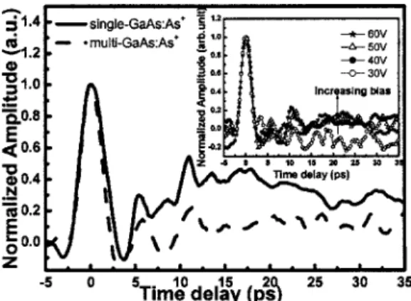
The full-width-at-half-maximum共FWHM兲 responses of the single- and multienergy-implanted GaAs: As+PCS
anten-nas are determined to be 3 and 2.7 ps, respectively共see Fig. 1兲. These correspond to 3-dB fast Fourier-transformed band-widths of greater than 150 GHz. The bias dependence of the photoconductive responses of the multienergy-implanted GaAs: As+PCS is shown in the inset of Fig. 1. The switching
speeds of both devices are similar, it is, however, worth not-ing that the trailnot-ing edges of the photoconductive responses of the multienergy-implanted GaAs: As+ PCS are greatly suppressed. In multienergy-implanted GaAs: As+ PCS with
60 V bias, the amplitude of the falling part is reduced to ⬍15% of the peak response as compared to that of the single-energy-implanted GaAs: As+ device 共which still re-mains as high as nearly 50%兲. The fall time 共1/e兲 of the single-energy-implanted GaAs: As+ PCS slightly increases from 1.3 to 2.3 ps as the bias voltage increases from 25 to 60 V. By contrast, no apparent bias dependence of the falling time response was observed 共⬃1.5 ps兲 for the multienergy-implanted GaAs: As+PCS共see the upper part of
Fig. 2兲. The longer falling time of the single-energy-implanted GaAs: As+is attributed to the insufficient trapping of photoexcited carriers coming from bulk SI GaAs under high pumping density.8 At higher bias, more photoexcited carriers in bulk SI GaAs with longer lifetime will also be collected, which inevitably increase the total response time of the single-energy-implanted GaAs: As+PCS. In contrast,
the multienergy-implanted GaAs: As+ has higher absorption
coefficient and trapping center density, which not only helps limiting the penetration depth of photons but also enhances the trapping of photoexcited carriers from bulk SI GaAs. With the multienergy recipe, the necessity of an electric-buffer layer between the arsenic-rich layer and bulk GaAs is relaxed. The uniformity of arsenic antisite defects distributed in multienergy-implanted GaAs: As+is believed to contribute
to the unchanged carrier trapping time as compared to single-energy-implanted GaAs: As+.
The dark current of a multienergy-implanted GaAs: As+
PCS antenna is relatively low as compared to those of single-energy-implanted and SI GaAs samples 共see lower part of Fig. 2兲. The multienergy-implanted GaAs:As+ PCS was
found to be highly resistive with ultralow dark current of 0.94A at a bias of 40 V. This is about one-half that of the single-energy-implanted GaAs: As+PCS. At still lower bias,
the dark current can be further reduced to 30 nA, which is far smaller than that of a PCS fabricated on a SI GaAs substrate. The multienergy-implanted GaAs: As+ exhibits
uni-formly distributed As precipitates and higher defect concen-trations at a cost of degradation in carrier mobility as well as optical responsivity. As shown in Figs. 3共a兲 and 3共b兲, the optical responsivity of a multienergy-implanted GaAs: As+ PCS at low pumping power is not as high as that of the single-energy-implanted GaAs: As+ sample. Owing to the lower density and the larger effective mass of free carriers in
FIG. 1. Normalized photoconductive response and of single-共solid line兲 and multi-共dashed line兲 energy-implanted GaAs:As+PCSs at a bias voltage of
60 V as measured by the EOS technique. The inset shows the normalized photoconductive response of multienergy-implanted GaAs: As+PCS at
dif-ferent bias voltages.
FIG. 2. Bias-dependent falling time共upper part兲 and dark current 共lower part兲 of single- 共circle dot兲 and multi- 共square dot兲 energy-implanted GaAs: As+PCSs.
013711-2 Liu et al. J. Appl. Phys. 98, 013711共2005兲
multienergy-implanted GaAs: As+, a much higher saturation
power can be expected for the multienergy-implanted GaAs: As+PCS. In Fig. 3共c兲, we have plotted the peak
am-plitude of photoconductive responses of multi- and single-energy-implanted GaAs: As+PCSs as a function of bias
volt-age. Clearly, that of the multienergy-implanted GaAs: As+
PCS exhibits a slower rising trend than the single-energy-implanted sample. Its magnitude, however, is eventually comparable to that of the single-energy-implanted device at a forward bias of ⬎100 V. The optical responsivity of a multienergy-implanted GaAs: As+ PCS at exciting power of
100 mW is 2 mA/ W, which is slightly lower than that of a single-energy-implanted GaAs: As+ PCS共5 mA/W兲.
None-theless, these responsivities are better than ever reported for the LT-GaAs-based sample 共1 mA/W兲.8At higher pumping powers 共⬎100 mW兲, the photoconductive response of the single-energy-implanted sample at lower biases saturates 共see Fig. 3兲. This can be explained by the intervalley carrier transfer共scattering of carriers from the ⌫ to L valley in the conduction band兲. In contrast, the response of a multienergy-implanted GaAs: As+ PCS does not saturate until much
higher bias共⬃90 V兲. The saturation fields are determined to be 25 and ⬎45 kV/cm for single- and multienergy-implanted GaAs: As+ samples, respectively. From these
re-sults, effective carrier mobilities for single- and multienergy-implanted GaAs: As+ are estimated to be 1480 and
590 cm2/ V s, respectively, according to the following
equation:14 I = ec P共1 − R兲 h Vbias d2 , 共1兲
where is the quantum efficiency, is the excitation effi-ciency, P is the average laser power, R is the reflectance coefficient, Vbiasis the bias voltage, his the photon energy
of the laser, and d is the width of the photoconductive gap. The smaller carrier mobility in multienergy-implanted GaAs: As+infers that the effective mass of electrons in these materials could be much larger, since it is inversely propor-tional to the carrier mobility共⬀e/ m兲.15,16The carrier trap-ping somewhat degrades the optical responsivity and
effec-tive carrier mobility of GaAs: As+, however, it greatly improves the switching response.
To evaluate the terahertz emitting properties of these ma-terials, planar photoconductive log-spiral antennas with metal-semiconductor-metal 共MSM兲 interdigitated electrodes were patterned on the single- and multienergy-implanted GaAs: As+ substrates. The finger width, area, and outer
di-ameter of the 1.5-turn GaAs: As+ PCS antennas are 5m,
35⫻35m2, and 300m, respectively. Biased at 10 V and
excited with 10 mW average power from a femtosecond mode-locked Ti:sapphire laser, the normalized terahertz ra-diation wave forms and frequency spectra detected using a LT-GaAs-based dipole antenna receiver6with probe power of 2.5 mW are shown in Figs. 4共a兲 and 4共b兲. The measured terahertz emission pulse widths of multi- and single-energy-implanted GaAs: As+ antennas are 0.8 and 1.2 ps,
respec-tively. The central frequencies 共and spectral linewidths兲 of multi-energy-implanted GaAs: As+ and
single-energy-implanted GaAs: As+are 0.2 THz共0.18 THz兲 and 0.15 THz
共0.11 THz兲, respectively. As a reference, those of a S.I. GaAs antenna were 0.14 THz 共0.1 THz兲. The single-energy-implanted GaAs: As+ antenna has a similar emission
re-sponse to the SI GaAs one except a slightly shrunken falling tail of the terahertz pulse shape. The trapping of photoexcited carriers from bulk SI GaAs becomes more pronounced after multienergy implantation. Notably, the shorter emission time of the multienergy-implanted GaAs: As+ antenna relies strongly on its fast photoconductive response. This extends the Fourier-transformed spectrum of the multienergy-implanted GaAs: As+antenna to a higher-frequency region.
IV. CONCLUSION
In conclusion, we report ultrafast 共⬃2.7 ps, instrument limited兲 switching responses of a multienergy-implanted GaAs: As+ photoconductive switches 共PCSs兲 with
sup-pressed trailing edge and reduced dark current. This material is highly resistive with dark current as low as 0.94A at a bias of 40 V, which is one-half that of single-energy-implanted GaAs: As+. The carrier mobility of the former is,
however, reduced to ⬃590 cm2/ V s, resulting in a small-signal optical responsivity of ⬃2 mA/W as compared to ⬃5 mA/W of the latter. Nonetheless, the
multienergy-FIG. 3. Optical responsivity of共a兲 single- and 共b兲 multienergy-implanted GaAs: As+ PCS at pumping powers of 30 共triangular兲, 70 共circle兲, and
100 mW共square兲. 共c兲 Peak amplitude of the transient photoconductive re-sponse from single-共circle dot兲 and multi- 共square dot兲 energy-implanted GaAs: As+PCSs at different bias voltages.
FIG. 4. The normalized terahertz radiation共a兲 wave forms and 共b兲 power spectra from SI GaAs共circle dot兲, single- 共dashed line兲 and multi- 共solid line兲 dose GaAs:As+PCS-based spiral antennas.
implanted GaAs: As+PCS pumped at 100 mW and biased at
80 V exhibits peak response共0.35 V兲 comparable to the best result of single-energy-implanted ones. This is attributed to the higher breakdown threshold of the multienergy-implanted GaAs: As+ PCS. The improvement on
photocon-ductive response is crucial for the generation of shorter tera-hertz emission pulses from spiral antennas fabricated on multienergy-implanted GaAs: As+ 共0.8 ps兲 than
single-energy-implanted GaAs共1.2 ps兲, with the central frequency blueshifted to 0.2 THz 共from 0.15 THz兲 and the spectral bandwidth broadened to 0.18 THz 共from 0.11 THz兲. The strong optical absorption and carrier trapping in the multidose-implanted GaAs: As+ layer is essential for the
shrinkage of the falling tail due to the effective suppression of residual carriers excited in bulk GaAs.
ACKNOWLEDGMENTS
This work was supported in part by the National Science Council of Taiwan under variant Grants and the Pursuit of Academic Excellence Program of the Ministry of Education of the ROC.
1N. M. Froberg, B. B. Hu, X. C. Zhang, and D. H. Auston, IEEE J.
Quan-tum Electron. 28, 2291共1992兲.
2E. R. Brown, K. A. McIntosh, F. W. Smith, K. B. Nichols, M. J. Manfra,
C. L. Dennis, and J. P. Mattia, Appl. Phys. Lett. 64, 3311共1994兲.
3A. C. Warren, N. Katzenellenbogen, D. Grischkowsky, J. M. Woodal, M.
R. Melloch, and N. Otsuka, Appl. Phys. Lett. 58, 1512共1991兲.
4S. Gupta, M. Y. Frankel, J. A. Valdmanis, J. F. Whitaker, F. W. Smith, and
A. R. Calawa, Appl. Phys. Lett. 59, 3276共1991兲.
5A. Claverie, F. Namavar, and Z. Liliental-Weber, Appl. Phys. Lett. 62,
1271共1993兲.
6F. Ganikhanov, G.-R. Lin, W. C. Chen, C. S. Chang, and C.-L. Pan, Appl.
Phys. Lett. 67, 3465共1995兲.
7A. Krotkus, S. Marcinkevicius, J. Janski, M. Kaminska, H. H. Tan, and C.
Jagadish, Appl. Phys. Lett. 66, 3304共1995兲.
8H. H. Wang, P. Grenier, J. F. Whitaker, H. Fujioka, J. Jasinski, and Z.
Lilienthal-Weber, IEEE J. Sel. Top. Quantum Electron. 2, 630共1996兲.
9G.-R. Lin and C.-L. Pan, Appl. Phys. Lett. 71, 2901共1997兲.
10G.-R. Lin, W. C. Chen, S. C. Chao, C. S. Chang, K. H. Wu, T. M. Hsu, W.
C. Lee, and C. L. Pan, IEEE J. Quantum Electron. 34, 1740共1998兲.
11T. A. Liu, M. Tani, and C.-L. Pan, J. Appl. Phys. 93, 2996共2003兲. 12T. A. Liu, M. Tani, M. Nakajima, M. Hangyo, and C.-L. Pan, Appl. Phys.
Lett. 83, 1322共2003兲.
13M. Lambsdroff, J. Kuhl, J. Rosenzweig, A. Axmann, and J. Schneider,
Appl. Phys. Lett. 58, 1881共1991兲.
14M. Tani, K. Sakai, and H. Mimura, Jpn. J. Appl. Phys., Part 2 36, L1175
共1997兲.
15S. Yngvesson, Microwave Semiconductor Devices 共Kluwer Academic,
Massachusetts, 1991兲, p. 9.
16A. Raymond, J. L. Robert, and C. Bernard, J. Phys. C 12, 2289共1979兲.
013711-4 Liu et al. J. Appl. Phys. 98, 013711共2005兲