Bandpass Filter of Serial Configuration With Two
Finite Transmission Zeros Using LTCC Technology
Chun-Fu Chang and Shyh-Jong Chung, Member, IEEE
Abstract—This study proposes a second-order bandpass filter of serial configuration. The filter schema incorporates a grounding capacitor, connecting the two conventional parallel LC resonators with the ground, to provide two finite transmission zeros. The impedance matrix and graphical solutions describe proposed filter’s operation principle. To demonstrate the proposed filter schema, two bandpass filters, with center frequencies of 2.44 and 4.8 GHz, were designed and implemented using low-temperature co-fired ceramic multilayer technology. The measured results were found to agree well with the simulation results. The 2.44-GHz fab-ricated bandpass filter was found to possess low in-band insertion loss and high out-band suppression, making it suitable in wireless local area networks, Bluetooth, and RF home links.
Index Terms—Bandpass filter, Bluetooth, finite transmission zeros, low-temperature co-fired ceramic (LTCC), RF home link, wireless local area network (WLAN).
I. INTRODUCTION
T
HE SWIFT development of mobile communication has made size and weight reduction, low cost, and high performance essential for RF products. To make a compact design of RF passive components, such as filters, baluns, matching circuits, and even antennas, can be implemented on a multilayer stack-up substrate. Other RF active compo-nents and baseband/digital circuitry can also be embedded on the same substrate to enhance product integration. This “system-on-package” concept of integrating many or all elec-tronic components of a functional system or a subsystem into one product has attracted considerable attention re-cently [1]–[4]. The increase in the design degree of freedom has resulted in small high-performance embedded passive components. The low-temperature co-fired ceramic (LTCC) technology is a very widely used multiplayer technology for designing miniaturized RF passive components, owing to its three-dimensional (3-D) integration capabilities, process tolerance, and low dielectric loss.The bandpass filter is one of the most important passive com-ponents in RF circuitry, attracting significant interest in 3-D miniaturized design [5]–[12]. A good bandpass filter has low passband insertion loss and provides large suppression in the rejection area including the image signal and in-band signal har-monics. High suppression in rejection area can be provided by generating transmission zeros at the rejection frequencies. A
Manuscript received September 3, 2004; revised November 30, 2004 and De-cember 31, 2004. This work was supported in part by the National Science Council, R.O.C., under Contract NSC 93-2752-E009-002-PAE.
The authors are with the Department of Communication Engineering, National Chiao Tung University, Hsinchu, Taiwan 30050, R.O.C. (e-mail: [email protected]).
Digital Object Identifier 10.1109/TMTT.2005.850414
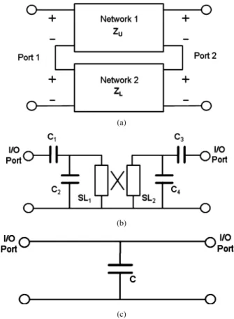
Fig. 1. Schema of the proposed bandpass filter with a grounding capacitorC forming a feedback path to produce two finite transmission zeros.
common approach to producing finite transmission zeros is to form a feedback path by adding a coupling capacitor between I/O ports [5], [8].
This study presents a bandpass filter of serial configuration with two finite transmission zeros, and demonstrates the filter using LTCC technology. The proposed filter is based on a con-ventional filter architecture with transmission zeros at dc and in-finite frequency, and incorporates a capacitor between the tra-ditional filter and ground, as shown in Fig. 1. The grounding ca-pacitor provides a feedback path to the common bandpass filter and, as explained below, generate two finite transmission zeros at different sides of the passband. Section II describes the pro-posed filter’s operation and validates its configuration function using the filter network’s impedance matrix [13] together with graphical solutions [5], [6]. Section III presents the 3-D layout of two LTCC bandpass filters with the proposed schema. The filters were designed and simulated using a full-wave electro-magnetic (EM) simulator. Section IV shows the measurement results of the two fabricated LTCC filters. The experimental and simulation results were found to agree. Finally, Section V briefly draws conclusions about this study.
II. THEORY
The proposed filter schema in Fig. 1 can be regarded as two two-port networks connected in series with the upper and lower parts shown in Fig. 2(a). The upper network (Network 1) can be a conventional bandpass filter with an infinite transmission zero, such as a bandpass filter with an equal-ripple or maximally flat response [13]. The filter schema chosen for this study is illus-trated in Fig. 2(b). The lower network (Network 2) is simply a shunt capacitor , as illustrated in Fig. 2(c). In the upper net-work, and the stripline section form a resonator, as do and the stripline . The two resonators can generate two poles supporting the filter’s passband. The coupled striplines
(b)
(c)
Fig. 2. (a) Representation of the proposed filter with two serially connected two-port networks. (b) The upper network (Network 1) without the grounding capacitor. (c) The lower network (Network 2) of a shunt grounding capacitorC.
and couple the major portion of signal energy be-tween the I/O ports close to the center frequency. Capacitors and act as inverters matching the resonators to the external impedance [13] and as dc-decoupling capacitors to block the dc signal at the front or back stage of the filter. As demonstrated below, this upper network behaves as a bandpass filter without finite transmission zeros if the grounding capacitor is omitted. The impedance matrix of the proposed filter configuration in Fig. 2(a) can easily be derived as the sum of the upper and lower network ) matrices, i.e.,
(1) These impedance matrices assumed the filter to be lossless and, thus, are purely imaginary, i.e., , where denotes the corresponding reactance matrix. Notably, for the simple lower network shown in Fig. 2(c), the elements of the impedance matrix are the same and can be derived as
(2) Network theory relates the scattering parameter (i.e., the transmission coefficient) of the filter to the impedance matrix elements by the following formula [13]:
(3) where represents the characteristic impedance of the I/O ports, set to 50 in this study. The finite transmission zeros of the filter are located at the frequency where
pacitor circuits and the inductor circuit, the matrix and, thus, the -matrix of the upper network can then be de-rived as follows:
(6) Finally, substituting (6) into (5) generates a fourth-order poly-nomial equation of as follows:
(7) whose two positive roots are the frequencies of the finite trans-mission zeros.
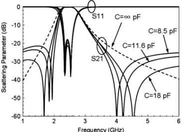
The characteristic (5) for transmission zeros can also be solved graphically. Fig. 3 depicts the left-hand side (solid line) and right-hand side (dashed lines) of (5) as frequency functions. The mutual reactance function of the upper network in Fig. 2(b) was calculated with the circuit simulator Microwave Office,1using a symmetrical geometry with pF
and pF. The striplines and had identical dimensions, 3.1 mm 0.1 mm (length width), with a narrow spacing of 0.1 mm to ensure sufficient mutual in-ductance. Fig. 3 compares five reactance curves for the lower network with the grounding capacitance varying from 8.5 to 18 pF. The filter’s transmission zeros, which obey relationship (5), correspond to the intersection points between the solid line and dashed lines. Clearly each grounding capacitance has two intersection points, i.e., two finite transmission zeros. Addi-tionally, the locations of the two transmission zeros expand outward as the grounding capacitance increases. The desired transmission zeros can be obtained for the bandpass filter by selecting appropriate grounding capacitance values.
Fig. 4 illustrates the computed return loss and inser-tion loss of the entire bandpass filter of Fig. 1. The solid lines denote the results for three grounding capacitances (
and pF), while the dashed lines represent those of the conventional filter structure [see Fig. 2(b)], which is equiv-alent to the proposed filter with infinite grounding capacitance
Fig. 3. Mutual reactance functionX of the upper network (network 1) and the negative of the mutual reactance0X (=1=!C) of the lower network (Network 2) in Fig. 2. The dashed lines denote grounding capacitances ofC = 8:5; 10; 11:6; 14; and 18 pF. The finite transmission zeros are located where the solid line intersects with the dashed lines.
Fig. 4. Scattering parameters (computed by the circuit simulator) of the proposed bandpass filter with different grounding capacitances (C = 8:5; 11:6; and 18 pF). The response of the conventional filter without the grounding capacitor (or withC = 1) is also given for comparison.
. The graph demonstrates that changing the grounding capacitance does not alter the filter’s passband, which remains the same as that of the conventional filter, i.e., connecting a grounding capacitor in series with a conventional filter does not influence the insertion and return losses in the passband. This phenomenon was also noted in the filter with a feedback capac-itor connecting the I/O ports [5]. Furthermore, Fig. 4 shows that each filter configuration with a grounding capacitor possesses two finite transmission zeros, one in the lower stopband and the other in the higher stopband. The frequency of the lower zero falls, while that of the higher zero rises, as the grounding capac-itance increases. At the limit, when the capaccapac-itance is increased to infinity, the transmission zeros converge to a dc zero and an infinite zero, as in the conventional filter. Significantly, the trans-mission zeros are located precisely at the intersection points in Fig. 3 for each grounding capacitance.
Equation (4) indicates that transmission zeros can be pro-duced by serially connecting two networks with positive and negative reactance. The proposed filter has an inductive upper network with positive reactance, and a capacitive lower network
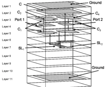
Fig. 5. 3-D LTCC layout of the 2.4-GHz bandpass filter. The dielectric constant of LTCC substrate for each layer is 7.8 (at 2.5 GHz), the loss tangent is 0.004 (at 2.5 GHz), and the silver alloy thickness is 0.02 mm. The top six LTCC substrate layers are 0.039-mm thick and others are of 0.087-mm thick.
with negative reactance. The lower network is used to form a feedback so as to produce finite transmission zeros. If the upper network is capacitive, then the lower network should be induc-tive with posiinduc-tive reactance [6].
III. LTCC LAYOUTS ANDEM SIMULATION
Based on the proposed filter schema, two bandpass filters with different passbands were designed and fabricated using the LTCC process. The first step is to adjust the filter’s com-ponent values with the circuit simulator to obtain the ideal fre-quency responses. Second, a multilayer LTCC structure is de-signed using the new component values, and simulated using the full-wave commercial package High-Frequency Structure Sim-ulator (HFSS),2which is a 3-D finite-element-based EM
simu-lator. At this stage, the mutual coupling of the filter components in the compact multilayer structure would result in different sim-ulation responses from those obtained initially. Therefore, the LTCC layout is finally fine tuned to minimize the difference be-tween the full-wave simulation results and the ideal results.
The first bandpass filter designed in this study is typically applied in Bluetooth or IEEE 802.11 b/g wireless local area network (WLAN), which has a passband bandwidth of nearly 100 MHz centered at 2.44 GHz. Besides low insertion loss in the passband, the filter should also produce a high rejection at 1.8/1.9 GHz and at around 4.9 GHz to suppress the DCS 1800 interference signal and the second harmonic of the operating quency. The filter has circuit component values with ideal fre-quency responses, as described in Section II, with the grounding capacitance pF.
After the second and third design steps, a 3-D layout of the first filter was obtained and shown in Fig. 5. The first filter con-tained ten LTCC layers. The top six layers were 0.039-mm thick, and the others were 0.087-mm thick. The thickness of the metal plates (silver alloy) was 0.02 mm. Since the grounding capacitor
metal plates on Layers 6 and 5. The capacitors and in the two resonators of the filter were produced by the plates on Layers 5 and 4. The stripline between and was con-nected to by Via 1 and connected to by Via 2. Notably, these two vias would contribute a small inductance to . Sim-ilarly, was connected to by Via 3 and connected to by Via 4. The striplines were located on Layer 9 with 0.1-mm spacing, considering the limitation of distance between two ad-jacent lines in fabrication. The required mutual inductance could be obtained using an appropriate coupling length. Significantly, the mutual inductance was formed by edge-coupled, instead of broadside-coupled, striplines. This coplanar layout would re-duce the inaccuracy in LTCC fabrication because the error prob-ability of metal offset in edge coupling is much smaller than that in broadside coupling. Furthermore, the edge-coupled striplines maintained the symmetry of the 3-D layout and, thus, the sym-metry of the filter functions.
The bottom layer (Layer 10) was a ground with the central part excavated in order to avoid the large parasitic grounding-capaci-tance effect between the two striplines and the ground. These three ground layers (Layers 1, 3, and 10) were connected by the side pads on the two longer edges of the LTCC substrate, and the I/O ports are on the shorter edges of the LTCC. The total size of the LTCC bandpass filter was 2.5 2.0 0.8 mm . Fig. 6 shows the full-wave EM simulation results for the 3-D LTCC layout, as com-pared to the ideal responses computed by the circuit simulator. The EM simulation results were found to agree with the ideal ones, except for higher insertion loss in the passband resulting from the conductor and dielectric losses considered in the EM simulation. These results demonstrate that the 3-D configuration is a good bandpass filter with low in-band insertion loss and high out-band rejection (larger than 30 dB) at 1.8/1.9 GHz and the second har-monic frequency (around 4.9 GHz). Fig. 6 also illustrates the EM simulation results for the LTCC layout without bottom ground ex-cavation. These results differ significantly from the EM simula-tion results for the layout with bottom ground excavasimula-tion, con-firming the strong parasitic grounding-capacitance effect on the filter performance.
The second bandpass filter was designed with a bandwidth larger than 0.9 GHz centered at the frequency of 4.8 GHz. Using the proposed filter schema in Fig. 1, an ideal bandpass filter response was obtained with pF,
pF, and pF. The dimensions (length width) of and were both 1.05 mm 0.15 mm. The spacing between striplines was set to 0.15 mm.
Fig. 6. EM simulated scattering parameters of the 2.4-GHz bandpass filter with (solid lines) and without (dotted lines) excavated bottom ground plane. The dashed lines denote the parameters computed by the circuit simulator.
Fig. 7. 3-D LTCC layout of the 4.8-GHz bandpass filter. The dielectric constant of LTCC substrate for each layer is 7.8 (at 2.5 GHz), the loss tangent is 0.004 (at 2.5 GHz), and the thickness of the silver alloy is 0.02 mm. The top seven layers of LTCC substrate are 0.039-mm thick, and others are of 0.087-mm thick.
In this case, all components were smaller in this bandpass filter than those in the 2.4-GHz bandpass filter. Therefore, this filter was realized in a smaller size of 2.0 1.2 0.88 mm with the 3-D LTCC layout revealed in Fig. 7. The LTCC had 11 layers; the top seven layers were 0.039-mm thick, while the other layers were 0.087-mm thick. This filter, being smaller than the previous filter, constructed the grounding capacitor using only the top two layers. Moreover, three layers were employed to construct and from Layers 3 to 5 with connecting the plates on Layer 3 to those on Layer 5 by vias forming two ver-tical interdigital capacitors. The striplines and on Layer 7 were respectively connected to and by vias and to each other at a buffer pad on Layer 6. The buffer pad was connected to the grounding capacitor through a via from Layers 6 to 2. The buffer pad reduced the total number of required vias, thus pushing cost down and increasing the fabrication yield. No-tably, the striplines were in parallel with the capacitors and formed between Layers 3 and 2. Additionally, the bottom
Fig. 8. Scattering parameters of the 4.8-GHz bandpass filter calculated by EM simulator (solid lines) and circuit simulator (dashed lines).
Fig. 9. Comparison of the measured (solid lines) and EM simulated (dashed lines) scattering parameters of the 2.4-GHz bandpass filter.
ground did not need to be excavated since the striplines’ layer was far from the bottom ground. Fig. 8 compares the EM sim-ulation results for the 3-D layout with the ideal responses cal-culated by the circuit simulator. These results agree with each other quite well.
IV. EXPERIMENTALRESULTS
After the analysis and EM simulation, the designed filters were fabricated using the Dupont 951 LTCC process with di-electric constant of 7.8 (at 2.5 GHz), loss tangent of 0.004 (at 2.5 GHz), and thickness of the silver alloy of 0.02 mm. The com-monly used printed-circuit board FR4 with a dielectric constant of 4.7, loss tangent of 0.02, and thickness of 0.4 mm was applied as the test board to measure the performance of the fabricated LTCC filters.
Fig. 9 shows the measured results for the 2.4-GHz bandpass filter, together with the EM simulation results. The two trans-mission zeros of the measured response occurred at 1.9 and 4.3 GHz, which are 100 MHz higher than in the simulation. Sig-nificantly, the zero at the high-skirt side on the measured result, which is much deeper than that of the simulation, can provide a signal suppression ) of 45 dB. Moreover, in the measured
Fig. 10. Comparison of the measured (solid lines) and EM simulated (dashed lines) scattering parameters of the 4.8-GHz bandpass filter.
results, the second harmonic of 2.4-GHz signal could be sup-pressed to 38 dB, and the suppression during 3.7–6 GHz was higher than 30 dB. The zero on the low-skirt side provided sup-pressions of 41 dB at 1.916 GHz, 38 dB at 1.9 GHz, and 27 dB at 1.8 GHz. The passband insertion loss from 2.4 to 2.483 GHz was better than 1.93 dB, with a minimum value of 1.7 dB at 2.48 GHz. The measured response agrees well with that of the EM simulation.
Fig. 10 compares the measured and EM simulated results for the 4.8-GHz bandpass filter. The measured response agrees well with the EM simulation response, except that the two fi-nite transmission zeros shifted slightly to higher frequencies in the measured response. In the measured results, the 1.5-dB in-sertion-loss bandwidth extended from 4.42 to 5.16 GHz, with a minimum value of 1.16 dB at 5 GHz. The suppression was 35 dB at the lower zero (3.75 GHz) and 50 dB at the higher zero (7.96 GHz). The 4.8-GHz bandpass filter had a larger passband fractional bandwidth, but a worse out-band rejection at the lower side of the passband, compared to the 2.4-GHz bandpass filter. This difference was found because the ratios of the zero loca-tion to the band edge for two designs are different. The closer the zero is to the band edge, the less the ultimate rejection will be got. In Fig. 9, the ratio of the lower zero to the lower band edge in the measured results is , while in the 4.8-GHz bandpass filter (Fig. 10), the ratio is
. Consequently, the 2.4-GHz filter has more ultimate re-jection at the low-skirt side owing to a farther zero than that of the 4.8-GHz filter. Fig. 11 presents a photograph of the two fab-ricated LTCC filters.
V. SUMMARY ANDFUTUREWORKS
In this study, a bandpass filter schema of serial configura-tion has been proposed and realized using the LTCC multi-layer process. In the proposed configuration, the method of pro-ducing two finite transmission zeros by the grounding capac-itor is entirely different from that by the traditional coupling ca-pacitor between I/O ports. Two bandpass filters with different passbands were designed and demonstrated. The circuit design, LTCC layout, EM simulation, and experimental results were
Fig. 11. Two fabricated LTCC filters. The photograph on the left-hand side shows the 2.4-GHz bandpass filter, and the photograph on the right-hand side one shows the 4.8-GHz bandpass filter.
thoroughly described. The measurement results were found to agree well with the EM simulation results. Both the fabricated bandpass filters were compact with low insertion loss in the passband and high suppression in the rejection area. Finally, the serial configuration design concept described in this study is clearly extendable to two networks with positive and nega-tive reactance to generate transmission zeros. A lower network with higher circuitry complexity is now under investigation to increase the design degree of freedom and/or obtain more trans-mission zeros.
ACKNOWLEDGMENT
The authors would like to thank the Mag.Layers Scientific-Technics Company Ltd, Hsin-Chu, Taiwan, R.O.C., for manu-facturing the two LTCC filters and for helpful discussions on the LTCC layouts. The authors further appreciate the reviewers for their valuable comments and suggestions.
This paper’s proposed filter schematic is patent pending. REFERENCES
[1] A. Sutono, D. Heo, Y.-J. E. Chen, and J. Laskar, “High-Q LTCC-based passive library for wireless system-on-package (SOP) module de-velopment,” IEEE Trans. Microw. Theory Tech., vol. 49, no. 10, pp. 1715–1724, Oct. 2001.
[2] N. K. Das and H. L. Bertoni, Eds., Directions for the Next Generation of
MMIC Devices and Systems. New York: Plenum, 1997, pp. 105–111. [3] C. M. Scanlan and N. Karim, “System-in package technology, appli-cation and trends,”, [Online]. Available: http://www.amkor.com/prod-ucts/notes_papers/.
[4] R. R. Tummala and V. K. Madisetti, “System on chip or system on package?,” IEEE Des. Test Comput., vol. 16, no. 2, pp. 48–56, Apr.–Jun. 1999.
[5] L. K. Yeung and K.-L. Wu, “A compact second-order LTCC bandpass filter with two finite transmission zeros,” IEEE Trans. Microw. Theory
Tech., vol. 51, no. 2, pp. 337–341, Feb. 2003.
[11] A. Simine, V. Piatnitsa, A. Lapshin, E. Jakku, D. Kholodnyak, S. Lep-paevuori, and I. Vendik, “Design of quasi-lumped-element LTCC filters and duplexers for wireless communications,” in Eur. Microwave Conf., vol. 3, Oct. 2003, pp. 911–914.
[12] W. Y. Leung, K.-K. M. Cheng, and K. L. Wu, “Multilayer LTCC band-pass filter design with enhanced stopband characteristics,” IEEE Microw.
Wireless Compon. Lett., vol. 12, no. 7, pp. 240–242, Jul. 2002.
[13] D. M. Pozar, Microwave Engineering, 2nd ed. New York: Wiley, 1998.
Chun-Fu Chang was born on February 1, 1982,
in Kaohsiung, Taiwan, R.O.C. He received the B.S. degree in communication engineering from the National Chiao Tung University, Hsinchu, Taiwan, R.O.C., in 2004, and is currently working toward the M.S. degree in communication engineering at the National Chiao Tung University.
He is currently involved with research on mi-crowave circuits, LTCC RF passive components, and LTCC front-end modules for WLAN applications.
Shyh-Jong Chung (M’92) was born in Taipei,
Taiwan, R.O.C. He received the B.S.E.E. and Ph.D. degrees from National Taiwan University, Taipei, Taiwan, R.O.C., in 1984 and 1988, respectively.
Since 1988, he has been with the Department of Communication Engineering, National Chiao Tung University, Hsinchu, Taiwan, R.O.C., where he is currently a Professor. From September 1995 to August 1996, he was a Visiting Scholar with the Department of Electrical Engineering, Texas A&M University, College Station. He was the leader of a sub-program in the four-year Advanced Technologies for Telecommunications National Research Program, which was sponsored by the Ministry of Educa-tion, Taiwan, R.O.C. He has authored or coauthored over 70 technical papers in international journals or conferences, including several invited papers and speeches. His areas of interest include the designs and applications of active and passive planar antennas, communications in intelligent transportation systems (ITSs), LTCC-based RF components and modules, packaging effects of microwave circuits, and numerical techniques in electromagnetics.