F4.
Design and VLSI Implementation of
MPEG
Audio Decoder
Tsung-Han Tsai Thou-Ho Chen Liang-Gee Chen
Department of Electrical Engineering
National Taiwan University National Taiwan University National Taiwan University Taipei, Taiwan, 106, R. 0. C. Taipei, Taiwan, 106, R. 0. C. Department of Electrical Engineering
Taipei, Taiwan, 106, R. 0. C.
Department of Electrical Engineering
Abstract-The paper presents a chip design for M P E G audio decoder, with a new modi- fied scheme. In the modified decoding scheme, the required computations can be reduced into half of the original one, and the storage demand too, i.e., the pseudo-QMF, a polyphase filter bank, only requires 512 words memory for 1024 points. Th e major operators include one adder- subtractor and one multiplier-accumulator. Th e chip is achieved by using the structure silicon compiler in the Genesil system, with 0.8-pm C- MO S technology.
INTRODUCTION D ata compression technique is an essential task for audio systems, which not only han- dles enormous amount of data, but also requires the high quality resolution. One of these au- dio coding techniques, MPE G (Moving Pictures Experts Group), a powerful audio compression standardization, undertakes the standardization of compression techniques for the associated au- dio [l]. It can significantly reduces the require- ments of transmission bandwidth and data stor- age, but with low distorsion.
Recently, there are some researches for audio decoding system [2], [3]. Although achieved
M-
P E G decoder by programming design method in a single chip, they also suffer from a considerable overheads of computation and control, based on the programmable demands.In our paper, we design a decoder-chip t o com- plete the decoding processes. According t o our approach for simplicity and low-cost design, we take use of the dedicated hardware approach (A- SIC), which provides a more efficient VLSI solu- tion. Especially, based on the computation anal-
ysis of MP E G decoding algorithm, we can re-
duce the computation amount of inverse MDCT into one-forth of t h e original one, which yield-
s half of the computation amount of t h e total MP EG decoding algorithm. Also, the proposed polyphase decomposition method only requires 512 words memory for 1024 points in inverse pseudo QMF. T h e proposed pipelined architec- ture of M PE G decoding algorithm satisfies the real-time requirements, with only one MAC and one adder/subtactor function units.
M P E G A U D I O C O D I N G
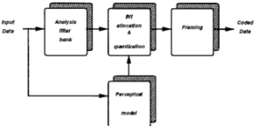
Th e elementary concepts behind M P E G is achieved by use of the perceptual coding, which exploits the properties of t h e human ear. Lat- erly, Subband/Transform coding can be used t o get the best performance at a very low bit rate Th e basic block diagram for MP E G audio en- coder is shown in Figure 1. Main blocks include the analysis filter bank, quantization and coding in the frequency domain, psychoacoustics mod- el and the assembly of output bit stream. T h e encoder accepts a continuous flow of input au- dio PC M samples. T he analysis filter bank, a polyphase filter bank, also named Pseudo-QMF (Pseudo-Quadrature Mirror Filter) [ 5 ] , creats a
mapping of the audio data into t h e same number of coefficients (or subsampled samples) in the spectral domain representation, with 32 eqnal- spaced subbands [6]. At this level, they are s-
caled and quantized in blocks within the bit- allocation module. Th e relevant coding param- eters are extracted and formatted into an encod- ed frame.
[41.
associated decoder recovers the encoded infor- mation frame by frame. Aft& the process of the frame unpacking, the iecoder performs an in- verse quantizing (expansion process), and feeds the subband synthesis filter bank with a set of
32 scaled-up subband samples in order t o recon- struct the output P C M audio signals, as shown in Figure 2 .
Figure 1: Block Diagram of the Encoder
Figure 2 : Block Diagram of the Decoder
T H E M O D I F I E D D E C O D I N G S C H E M E Starting from detail analysis about the com- putation complexity of M P E G decoder, we can improve the system performance by reducing the computation power, and schedule the data flow in order to get a more efficient algorithm. T h e MP E G decoding flow chart is shown in Figure
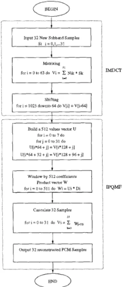
3 . I t includes some function block: decoding of side information, inverse quantization, synthesis subband filter bank, etc. Within the synthesis subband filter bank, t h e inverse Modified Dis- crete Cosine Transform (IMDCT), inverse Pseu- do Quadrature Mirror Filter ( I P QMF) will be realized, as shown in Figure 4.
For audio signal processing applications, one appropriate measure t o represent the complexity of a system would be million operations per sec- ond (MOPS ,where a operation is defined as da- t a access, store, add, shift, or multiply). Based
on this definition, the required signal processing computation amount for various components of MP EG decoder process is illustrated in Table 1.
According t o the illustration in Table 1, IMD- C T is the most computationally intensive opera- tion. This takes about two-t'hird of the required signal processing computation of the M PE G de- coder.
T h e original inverse MDCT of a sequence
S(IC), is defined as following: 31 (16
+
i ) ( 2 k+
l ) a l*
sk = cos[-- 64 k=O i = 0 , 1 , ... 6 3 IC = 0 , 1, ... 31Taking the advantage of t h e symmetric prop- erties:
cos
o
=cos(z.rr
-e)
T h e inverse MDCT definition equations can be leaded into a new formula with a reduction of the computation amount. 'Thus, t h e enhanced algorithm is listed as following:
( 3 2
+
i)(2IC+
l ) a 15-1
*[ S k f ( -l)i*s31- k]v,
= C c o s [ - 64 k = O i = 0 , 1,...
31IC
= 0, 1, ... 115This means that the size of summations is re- duced from 32 t o 16, and the number of sum- mations is also reduced from 64 t o 3 2 . As a
result, the number of multiplications and addi- tions can be reduded by a factor of 4. T h a t is,
Table 1: coder
Computation Power for M PE G De-
I PQM F
INPUTENWDQ SCALEPACTOR REQUANTIZATION OFSAMPLES
i
SYNTHESIS SUBBANDFigure 3: Decoding Flow Chart
the total computation amount for the decoding flow can be reduced into half of the original one. For the same reason, the required size for co- efficient ROM can be reduced as a factor of 4. Besides, the required size for the RAM buffer in which the inverse transformed d a ta V is stored can be reduced only to 512 words, instead of the original size of 1024 words. This algorithm is al- so based on our balance consideration between the high efficiency and simple implementation for VLSI solution.
ARCHITECTURE D ESI GN A N D VLSI IMPLEMENTATION Based on our approach for simplicity and low- cost design
,
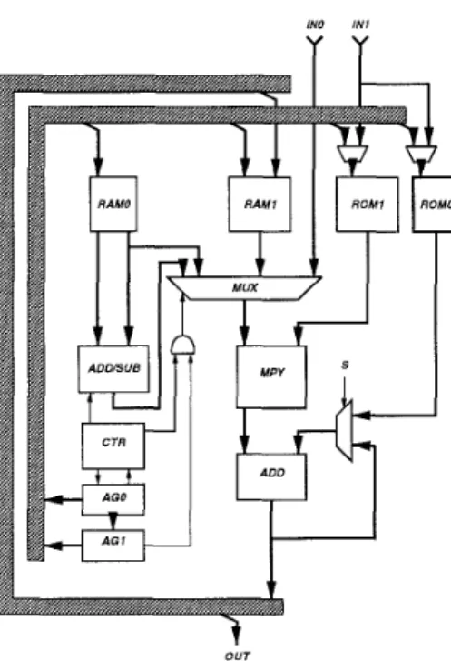
dedicated hardware design (ASIC), which offers a more efficient VLSI solution, is provided for our hardware design methodology. Figure 5 describes the overall hardware struc- ture for our proposed design. The data to be processed in the computation unit are held in 4 blocks of memory, as named: ROMO, ROM1, RAMO, RAM1. The ROMO is stored the co- efficients used in the inverse quantization pro-=
I "
IPQMF
Figure 4: Synthesis Subband Flow Chart
cess. The ROM1 is mainly stored as the 512- word cosine coefficients, and 512-word window coefficients. As a result, it contains above 1 K words. The 32-word RAMO is a dual-port d a ta memory which can access two d a ta simultane- ously. Thus this design can be realized about the butterfly-pair computation of the IMDCT pro- cess with a reduced overhead for memory access. The 512-word RAM1 represents as the IMDCT output buffer and also the I P Q MF input buffer. All these memory banks are designed as 24 bit word-lenght.
Besides, the proposed architecture can be scheduled as several function blocks. For the controller (CTR), we decide to take use of a
IN0 IN1
Y Y
t
OUT
Figure 5: Overall Hardware Structure
hard-wired architecture design for our simple and high efficient approach. Then it doesn't need a program memory and the requirement of some decoding operation, too. Also, in or- der t o enhance the throughput for the system, we take use of the pipeline schedule as a ef- ficiently strategy [ 7 ] . For the computation u- nit, there are only one adder-subtractor (AD- D/SUB) and one multiplier-accumulator (MAC) needed in this design. In addition, we design t- wo address generators to supply the memory ad- dress, which also reduce the overhead of the con- troller. Meanwhile, the AGO (Address Genera- tor 0) provides the memory address for ROMO, ROM1 and RAMO. These address is continu- ously calculated and broadcasted t o these three memory modules. By means of a multiplexer, t h e correct data would be passed successfully. In order to complete the shifting operations which represent the polyphase decomposition, we de- sign a dedicated address generator t o reduce the complexity of t h e operation. That is, the pur- pose for the AG1 (Address Generator l) is t o
generate the correct memory address for RAM1. The proposed design is implemented by the GENESIL silicon complier system, as shown in Figure 6. T h e chip takes use of the 0.8-pm CMOS technology. I t consists of 174973 tran- sistors in a size of 7.6 mm x 6.7 mm. The clock rate is 11.5 MHz, or 87 ns per icycle, which can match the requirements of t h e IDPEG decoding flow. T h e chip specification is lmted in Table 2.
Figure 6: Layout for the Proposed Chip
Table 2: Chip Specification
I
Technoloev11
0.8 um1
7.6 m m x 6.7 m m Transistor count Power dissipation 9 5 2 m W Pa d count CONCLUSIONSIn this paper, we introduce the MP E G codec. Later, we describe the detail analysis about the function complexity of MP EG decoder system, and adopt the decoding system with our im- provements in a lower rate of computation com- plexity. Based on the improved algorithm, the
goal for simplicity a nd low-cost designa is real- ized. Finally, th e dedicated circuit with an effi- cient architecture of pipeline scheme is obtained. This proposed chip is verified and realized by t h e GENESIL silicon complier system.
REFERENCES
[l] M P E G , "IS0 CD 11172-2: coding of mov- ing pictures and associated audio for digital storage media at u p t o about 1.5 Mb/s", Nov 1991
G. Maturi, "Single chip M P E G audio de- coder", IEEE Transactions on Consumer Electronics, vol. 38, No. 3, pp.348-356, Aug. 1992.
[3] F. Witte, R. Backes and M. Klumpp, "Mul- tipurpose audio signal compander", IEEE
Transactions on Consumer Electronics, vol. 39, No. 3, Aug. 1993.
[2]
[4] D. Scitzer, T h . Sporer, "Digital coding of high quality audio",IEEE Int. Conf. o n Acoustics, Speech a nd Signal Proc., 1991. [5] J. H. Rothweiler, "Polyphase quadra-
tu re filters- a new subband coding tech- nique",IEEE Int. Conf. on Acoustics, Speech an d Signal PTOC., 1983.
[6] Y. Francois. M. Lever and P . Urcun, "A MUSICAM source codec for digital au- dio broadcasting and storage",IEEE CClT-
T conf, 1991.
[7] K . Aono, M. toyokura and T. Araki, " A video digital signal processor with a vector- pipelind architecture", IEEE Journal of
Solid-State Circuits