行政院國家科學委員會專題研究計畫 期中進度報告
氮基三五族半導體奈米結構(2/3)
期中進度報告(精簡版)
計 畫 類 別 : 個別型 計 畫 編 號 : NSC 94-2120-M-110-002- 執 行 期 間 : 94 年 08 月 01 日至 96 年 02 月 28 日 執 行 單 位 : 國立中山大學物理學系(所) 計 畫 主 持 人 : 杜立偉 共 同 主 持 人 : 羅奕凱、蔡民雄、劉全璞 處 理 方 式 : 本計畫可公開查詢中 華 民 國 96 年 03 月 18 日
Buffer controlled GaN nanorods growth on Si(111) substrates by
plasma-assisted molecular beam epitaxy
Abstract
Size, shape, and density of self-assembled GaN nanorods grown on Si(111) substrates by plasma-assisted molecular beam epitaxy were successfully controlled by inserting a GaN buffer layer. The structure of the GaN buffer layer plays a vital role in the nanorod growth. Only a broken buffer layer with a suitable opening size can grow nanorods. Evolution of the nanorod is traced to the initial growth stage. Crystal seed grown at the wall of the opening in the buffer layer initiates the beginning of the nanorod, and a self-catalytic vapor-liquid-solid process, triggered by the nanocapillary condensation effect, enhances the GaN nanorod growth. Furthermore, the nanorod density can be largely controlled by using the beam equivalent pressure of the N/Ga ratio. Other GaN nanostructures grown at different growth conditions are also discussed in details.
INTRODUCTION
Low-dimensional nanometer-scale objects have attracted extensive interest in the past decade because of their enormous potential for various electronic and optoelectronic nanodevice applications.1-4 High performance nanodevices based on
GaN of high crystal quality are especially attractive as GaN and other related nitrides have many unique properties unavailable from other material systems, such as the wide and direct bandgap, chemical stability, high radiation hardness, and capability for high temperature operation,5-10 just to name a few. As reported in the literature,
many nanometer-scale GaN structures, for example, nanoparticles,11 nanowires,12,13
nanotubes,14,15 nanopillars,16,17 nanocolumns,18-24 and nanorods25-27 have been made
by various methods. Vertical GaN nanorods and nanocolumns grown on certain substrates are useful material structures, from an application point of view, because well-established traditional multilayered or heterostructural materials can possibly be fabricated on their tops. Practical application of the GaN nanorods include ultraviolet, blue, green, and white light-emitting diodes (LEDs), laser diodes (LDs), nano-sized vertical-cavity surface-emitting laser (VCSEL), and many others.28-30 In order to
increase the availability of nanomaterials, many researchers have attempted to control the rod density and lateral width because different specifications have different
applications. Dense nanorods can be practically applied to highly luminescent devices, such as high brightness LEDs, because of its highly crystalline quality and large emissive area.28 Isolated nanorods, with rather low rod density, are very suitable to be
fabricated as a single nanodevice, and many physical properties can be extracted from a single nano-object.29,30 Although there have been many reports in the literature on
the growth of GaN nanocolumns and nanorods, there seems to be no coverage of the full spectrum of evolving nanostructures.18-27 The intricacy of growth conditions in
relation to the resultant material structures hence continues to be an intractable problem.
Recently, GaN nanorods and nanocolumns grown on different substrates with or without a buffer layer, such as AlN/Al2O3,18-20 GaN/Al2O3,21 AlN/Si(111),21,22
SiO2/Si(001),23 SiC/Si(111),24 and Si(111)27 etc., have been studied, but no special
differences are observed between the use of these substrates. Appearance of these 1-dimensional (1D) nanorod-like structures in their reports is always dominated by changing the beam equivalent pressure (BEP) of the N/Ga ratio and the growth temperature. However, not only these two parameters but also the buffer layer structure can affect the GaN nanorod growth. In previous reports, nanorods grown directly on a substrate or a flat buffer layer controlled by the effective NBEP/GaBEP
condition) and low density to large diameter (slightly N-rich condition).18-27 But, the
control of specific rod density, diameter, and shape should be studied further. In this article, the GaN nanorod growth was well controlled by inserting a GaN buffer layer under different growth conditions, and many combinations of the rod density and diameter were obtained. Additionally, a comprehensive study has been conducted in an effort to understand the structural evolution from the nearly 2-dimensional (2D) epilayer to various sophisticated nanostructures.
I. EXPERIMENTAL DETAILS
GaN nanorods and related nanostructures were grown on n+-Si(111) substrate by
plasma-assisted molecular beam epitaxy (PAMBE). The PAMBE instrument is a Veeco-Applied EPI 930 system with liquid nitrogen cryopanel cooling. The growth chamber was evacuated down to a base pressure of 3 x 10-11 torr by a combination of
roughing pump, turbomolecular pump, and cryopump. 7N5 pure Ga metal was vaporized with a standard Knudsen effusion cell. 6N pure N2 was further purified
through a chemical purifier (Aeronex) and then fed into a radio-frequency (RF) plasma generator. Both Ga vapor and nitrogen plasma flux were measured with a beam flux gauge. Every effusion cell was equipped with a pneumatic shutter to
control the sample growth. The Si substrate was cleaned with acetone, isopropanol, and deionized (D. I.) water in an ultrasonic bath to remove residual organic contamination on the surface. To remove surface native oxides, chemical dipping in a HF : H2O = 1 : 5 solution, the concentration of the HF solution before dilution is 48 %,
for 5 minutes was applied. After chemical dipping, the substrate was again cleaned with D. I. water. After the chemical cleaning process, Si substrate was loaded into the buffer chamber, and then transferred into the growth chamber with the transfer arm. The Si substrate was annealed at 900 ℃ for 30 min in the growth chamber before the growth of GaN nanostructures. A clear ( 1 x 1 ) Si reflection high-energy electron diffraction (RHEED) pattern with Kikuchi lines were observed. After cooling down to 760 ℃, the RHEED pattern showed a clear ( 7 x 7 ) surface reconstruction pattern.31 This pattern indicated that the native oxides had been removed from the Si surface. Then, the GaN nanostructures were grown under different conditions. After the GaN nanostructures growth, field-emission scanning electron microscopy (FESEM) was applied to analyze the surface morphology. In order to show more information, these samples were often tilted 20 degrees from the surface’s normal direction or the cross-sectional surface.
II. RESULTS AND DISCUSSIONS
A. Variety of the GaN nanorods controlled by the GaN buffer layer
Various GaN nanorod structures with different sizes, shapes, and densities are shown in Fig. 1, and classified in two different structural groups. One is a dense nanorod structure, and the other structure is isolated nanorods, which are well separated and extruded above the surrounding matrix. Growth conditions and rod structures of these samples (A1 - A6) are listed in Table I. Only sample A6 was directly grown on Si(111) substrate with the same rod growth conditions, which were with temperature of 720 ℃, growth time of 5 h, and a NBEP/GaBEP ratio of 40. GaBEP
values of 2.5 x 10⁻⁷ torr and of 8.0 x 10⁻⁸ torr were used for the growth of the nanorod
and the buffer, respectively, and the NBEP was proportional to the GaBEP. The RF
power of the nitrogen plasma was always set at 500 watts for both the growth of the buffer and nanorod. Among the isolated nanorod structures, the GaN nanorods (sample A3), grown on a suitable buffer layer with a growth temperature of 600 ℃, show regular shapes and an uniformly lateral width distribution, but the others (samples A2 and A4) show non-regular shapes and a wide lateral width distribution. From the surface FESEM images, regular nanorods show hexagonal shapes with flat
surfaces, and they are always accompanied with a six-fold symmetrically V-shaped crater growth.26 Non-regular nanorods have a variety of shapes, such as triangular,
rectangular, pentagonal, and hexagonal shapes, and craters with similar shapes also accompanied the rod growth. However, the non-regular nanorods are mostly shorter and wider than the regular nanorods. No specific shape can be concluded from the dense nanorods (samples A1, A5, and A6). These nanorods were grown from the substrate surface without a surrounding matrix. This morphological change, the isolated nanorod structure translated into the dense nanorods, is merely due to the use of different buffer structures. This result indicates that the buffer layer has a vital role not only in epifilm growth32-34 but also in nanorod growth.
Figure 2(a) shows that the distribution of the GaN nanorod lateral width depends on buffer layer temperature. These statistic results, fitted by a Gaussian formula, show that the nanorods grown on the buffer layer at a temperature of 600 ℃ (sample A3) have the smallest lateral width and the narrowest width dispersion. The peak of the width distribution curve and the full width at half maximum (FWHM) of the curve which were fitted by a Gaussian formula from the sample A3 are 61.1 nm and 24.2 nm, respectively. As the buffer temperature moves away from 600 ℃, both the peak and the FWHM become wider. The rod density, peak and FWHM of the rod distributions are plotted in Fig. 2(b). As a comparison, sample A6 grown without
buffer layer (hollow symbols) is added into the Fig. 2(b) and treated as grown on a buffer with a temperature of 720 ℃. Densities of the dense nanorods are all almost the same, namely ~ 2 x 109 cm-2, but isolated nanorods have rather small densities in
the range of 1 x 10⁷ to 2 x 108 cm-2, depending on the buffer condition. Conspicuously,
only a buffer grown at the medium temperature range promotes isolated nanorod growth with thinner width, better width uniformity, and lower rod density. In earlier reports, 18-22 high density/small diameter (< 100 nm) and low density/large diameter
(≥ 100 nm) nanorods were fabricated on different substrates by tuning the effective NBEP/GaBEP ratio. The effective NBEP/GaBEP ratio can be adjusted through adjusting the
nominal NBEP/GaBEP ratio, the RF power, and the growth temperature. Furthermore,
by inserting a GaN buffer layer, low density/small diameter, low density/large diameter, and high density/large diameter nanorods were achieved in this study.
B. Evolution of the GaN nanorods from buffer layer
Three major morphologies of the GaN buffer layer grown on the Si(111) substrates are shown in Fig. 3. Buffers A1, A3, and A5 grown at temperatures of 460 ℃, 600 ℃, and 690 ℃ show a granular structure [Fig. 3(a)], a broken film [Fig. 3(b)], and isolated islands [Fig. 3(c)], respectively. The granular and the isolated
island structures lead subsequent films into densely nanorod structures, because the role of these 3D islands is to act as nucleation sites to assist the nanorod growth. Fig. 3(b) shows that many openings were formed in the buffer layer with sizes in a range of 5 nm to 100 nm. In some large openings (>20 nm), a pad grown at the sidewall of the openings maybe serve as a crystal seed for the isolated nanorod growth. To further study the isolated nanorod growth, different growth times were carried out to trace the regular nanorod growth by using sample A3 growth condition. After 30 minutes growth, as shown in Figs. 4(a) and 4(b), a large number of rods standing on the sidewall of craters become prominent with an almost equal height to the surrounding matrix. Fig. 4(c) shows the top-view image of a regular hexagonal rod in the center of a crater with a three-hour growth. Both the rod size and the crater size are larger than that obtained after 30 min growth. In Fig. 4(d), a lateral view image shows that the “rod” is embedded inside a large V-shape opening of a vertical trench. The inset of Fig. 4(d) shows that the root of the rod is in a cave (large opening) and stands on a pad near the GaN/Si interface. This indicates that the broken buffer film offers a very important environment to promote the nanorod growth inside the large opening.
Figure 5 show the relationships of matrix thickness, rod height, and rod density with different growth times. Both the matrix and the rods show a linear relationship between the height (thickness) and growth time, and they keep nearly constant growth
rates. The dependence of the densities of nanorods on growth time is nonlinear. The rod density increases very fast when growth time changes from 10 min to 30 min. It may be due to the rod height being lower than the matrix thickness for periods less than 10 min, which makes them difficult to be seen and counted. When the rod protrudes above the matrix, it becomes prominent to be identified as shown in Fig. 4(a). The largest rod density is 2.1 x 108 cm-2 after one-hour growth, which is slightly
smaller than the density of pads (3.3 x 108 cm-2) appeared in a large opening. With
increase of the growth time, the nanorod density decreases. The nanorod density decreases about 2 orders of magnitude after 20 h growth in comparison to the 30 min growth. This is owing to the fact that some neighboring nanorods coalesce with each other when the distances between these nanorods are too short to grow independently after a long-time growth. This coalescent phenomenon can also be seen in dense nanorods from the cross-sectional SEM images. In summary, density of pad grown in large openings at zero-minute growth, that is, at the buffer layer, is comparable to the maximum density of the nanorods. This result supports the view that the pad serves as a crystal seed to assist the nanorod growth. That is to say, the maximum rod density is determined by the initial growth stage.
Various GaN morphologies grown on the same buffer structure (buffer A3) with different NBEP/GaBEP ratios during the nanorod growth are shown in Fig. 6. Their
corresponding growth conditions are listed in Table II. These structures vary from matrix only (sample B1) to nanorod with matrix (sample B2), to nanorod with broken matrix (sample B3), and to nanorod with nanocomb structure (sample B4) as the NBEP/GaBEP ratio is changed from 10 [Fig. 6(a)] to 30 [Fig. 6(b)], to 50 [Fig. 6(c)], and
to 70 [Fig. 6(d)], respectively. Noteworthy, the GaN nanorod that coexisted with the nanocomb structure is quite different from the results of M. Yoshizawa et al.,18 E.
Calleja et al.,21 and Y. S. Park et al.27 because they showed only rod-like structures
under N-rich condition. In this series of experiment, basically, the growth rate of the GaN base matrix and nanorod increase as the NBEP/GaBEP ratio increase to 70, and
both reach a constant thickness/height at higher NBEP/GaBEP ratios. With respect to rod
width, the rod width is between 20 nm and 100 nm, with most rod widths between 40 nm and 70 nm when NBEP/GaBEP ratio is in the range of 30 - 50. No obvious
difference of the rod width is observed in this range of NBEP/GaBEP ratios. But, a very
different phenomenon is that the nanorod density increases one order of magnitude as the NBEP/GaBEP ratio increased from 30 to 50.
matrix growth similar as thin film growth. From a density-functional theory calculation, it was concluded that while Ga is very mobile at typical growth temperatures, diffusion of N is slower by several orders of magnitude.35 Excess N
strongly increases the Ga diffusion barrier, and surface diffusion length of the Ga and the N adatoms dominates the structure evolution.32-34 Within an intermediate Ga-rich
condition (without Ga droplets), excess Ga forms a steady layer without Ga droplets, and less N adatoms covers the substrate surface and encourages Ga adatoms to travel for a longer distance to promote the film growth with a 2-dimensional like growth mode. Although the GaN film is still grown with a 3-dimensional (3D) hillock structure, as shown in Fig. 6(a), which is caused by a large lattice mismatch (~ 17 %) between GaN and the Si substrate,26 the lateral growth rate is high enough to let the
nearby 3D islands to coalesce with each other, and no nanorod can be grown. On the contrary, with a large amount of N adatoms accumulated on the surface the diffusion of the Ga adatoms under N-rich condition is inhibited, and the matrix becomes a broken film and even develops to a nanocomb structure at higher NBEP/GaBEP ratio.
Although a GaN nanorod is grown under N-rich condition, the local environment of the crystal seed in a large opening after the buffer growth can accumulate more Ga adatoms by the nanocapillary condensation effect to form a Ga cluster to start the self-assembled process.36 A GaN nanorod grows faster along <0001> via the
vapor-liquid-solid (VLS) mechanism37 via reaction of the nitrogen plasma with Ga
liquid clusters while its surrounding GaN islands also grow alongside to form the base materials, though at a slower growth rate. Hence, under a slightly N-rich condition, a GaN nanorod grows along the vertical direction with a growth rate GR, which is faster
than the lateral growth rate of the surrounding matrix, GM-L, as shown in Figs. 6(b)
and 6(c). Furthermore, under highly N-rich condition, though surface diffusion of Ga adatoms is strongly inhibited by the N adatoms, the vertical growth rate of the surrounding matrix is higher than the lateral growth rate, which leads to a nanocomb structure growth, as shown in Fig. 6(d).
Growth diagrams of the GaN nanorod and surrounding matrix are sketched in Fig. 7. At the beginning, the Ga adatoms accumulate on crystal seeds to start a self-catalytic process in large openings triggered via the nanocapillary condensation mechanism [Fig. 7(a)].35 Three major morphologies can be discussed via a
combination of the parameters of GR, GM-L, and GM-V, the vertical growth rate of the
surrounding matrix. When the GM-L is bigger than the GR, no nanorod can protrude
above the matrix [Fig. 7(b)]. GaN nanorods start to protrude above the surrounding matrix when the GM-L is slightly smaller than the GR [Fig. 7(c)]. In Fig. 7(d), GM-L is
much smaller than GR, and GM-V is similar to the GR. Utilizing the competition
NBEP/GaBEP ratio during the nanorod growth. Combined with the buffer structures, the
sizes, the shapes, and the densities of the GaN nanorods are more controllable in the self-assembled process, similar to as the metal-catalyzed VLS process, in which the diameter of the wire was controlled by the size of the metal catalyst.12,37
III. SUMMARY AND CONCLUSIONS
Various GaN nanorod structures grown on a Si(111) substrate are realized by PAMBE. Evolution of the nanorod structure from isolated regular nanorods, to isolated non-regular nanorods, and to dense nanorods is well controlled by the GaN buffer structure. Adding the parameter of NBEP/GaBEP ratio to the nanorod growth, the
density of the regular nanorods becomes also a controllable item. There are several combinations of rod density and diameter in the nanorod growth. High density/small diameter and low density/large diameter nanorods can be grown directly on the surface without a buffer layer.18-21 Low density/small diameter, low density/large
diameter, and high density/large diameter nanorods can be achieved by inserting a GaN buffer. A growth mechanism of the isolated nanorods, grown by a buffer assistant, is presented as based on the experimental facts that the crystal seeds grow inside large openings in a broken buffer film, and that the nanorods grow faster than
the surrounding matrix via self-catalytic VLS process, which is triggered by the nanocapillary condensation.
REFERENCES
1 K. Hiruma, T. Katsuyama, K. Ogawa, M. Koguchi, H. Kakibayashi, and G. P.
Morgan, Appl. Phys. Lett. 59, 431 (1991).
2 A. M. Morales and C. M. Lieber, Science 279, 208 (1998).
3 F. Qian, Y. Li, S. Gradečak, D. Wang, C. J. Barrelet, and C. M. Liber, Nano Lett. 4,
1975 (2004).
4 H. M. Kim, Y. H. Cho, H. Lee, S. I. Kim, S. R. Ryu, D. Y. Kim, T. W. Kang, and K.
S. Chung, Nano Lett. 4, 1059 (2004).
5 M. H. Huang, S. Mao, H. Feick, H. Yan, Y. Wu, H. Kind, E. Weber, R. Russo, and P.
Yang, Science 292, 1897 (2001).
6 Y. Huang, X. Duan, Y. Cui, Lincoln, J. Lauhon, K. H. Kim, and C. M. Lieber,
Science 294, 1313 (2001).
7 H. Morkoc and S. N. Mohammad. Science 267, 51 (1995).
8 S. C. Shi, C. F. Chen, S. Chattopadhyay, Z. H. Lan, K. H. Chen, and L. C. Chen,
Adv. Funct. Mater. 15, 781 (2005).
Jpn. J. Appl. Phys. Part 2 44, L1076 (2005).
10L. W. Tu, P. H. Tsao, K. H. Lee, I. Lo, S. J. Bai, C. C. Wu, K. Y. Hsieh, and J. K.
Sheu, Appl. Phys. Lett. 79, 4589 (2001).
11Y. Xie, Y. Qian, W. Wang, S. Zhang, and Y. Zhang, Science 272, 1926 (1996).
12M. S. Gudiksen and C. M. Lieber, J. Am. Chem. Soc. 122, 8801 (2000).
13X. Chen, J. Li, Y. Cao, Y. Lan, H. Li, M. He, C. Wang, Z. Zhang, and Z. Qiao, Adv.
Mater. 12, 1432 (2000).
14J. Goldberger, R. He, Y. Zhang, S. Lee, H. Yan, H. Choi J, and P. Yang, Nature 422,
599 (2003).
15W. Han, S. Fan, Q. Li, and Y. Hu, Science 277, 1287 (1997).
16Y. D. Wang, S. J. Chua, S. Tripathy, M. S. Sander, P. Chen, and C. G. Fonstad, Appl.
Phys. Lett. 86, 071917 (2005).
17Y. Inoue, T. Hoshino, S. Takeda, K. Ishino, A. Ishida, H. Fujiyasu, H. Kominami, H.
Mimura, Y. Nakanishi, and S. Sakakibara, Appl. Phys. Lett. 85, 2340 (2004).
18M. Yoshizawa, A. Kikychi, M. Mori, N. Fujita, and K. Kishino, Jpn. J. Appl. Phys.
Part 2 36, L459 (1997).
19M. Yoshizawa, A. Kikuchi, N. Fujita, K. Kushi, H. Sasamoto, and K. Kishino, J.
Crystal Growth 189/190, 138 (1998).
Phys. Solid State 43, 151 (2001).
21E. Calleja, M. A. Sánchez-García, F. J. Sánchez, F. Calle, F. B. Naranjo, E. Muñoz,
S. I. Molina, A. M. Sánchez, F. J. Pacheco, R. García, J. Crystal Growth 201/202, 296 (1999).
22E. Calleja, M. A. Śanchez-Garćia, F. J. Śanchez, F. Calle, F. B. Naranjo, and E.
Muňoz, Phys. Rev. B 62, 16826 (2000).
23T. Yamashita, S. Hasegawa, S. Nishida, M. Ishimaru, Y. Hirotsu, and H. Asahi, Appl.
Phys. Lett. 86, 082109 (2005).
24J. Ristic, M. A. Sánchez-García , E. Calleja, A. Pérez-Rodríguez, C. Srre, A.
Romano- Rodríguez, J. R. Morante, V. R. Koerler, and W. Skorupa, Mater. Sci. Eng. B 93, 172 (2002).
25H. M. Kim, D. S. Kim, D. Y. Kim, T. W. Kang, Y. H. Cho, and K. S. Chung, Appl.
Phys. Lett. 81, 2193 (2002).
26L. W. Tu, C. L. Hsiao, T. W. Chi, I. Lo, and K. Y. Hsieh, Appl. Phys. Lett. 82, 1601
(2003).
27Y. S. Park, C. M. Park, D. J. Fu, T. W. Kang, and J. E. Oh, Appl. Phys. Lett. 85, 5718
(2004).
28H. M. Kim, Y. H. Cho, H. Lee, S. I. Kim, S. R. Ryu, D. Y. Kim, T. W. Kang, and K. S.
29J. Ristic, E. Calleja, A. Trampert, S. Fernández-Garrido, C. Rivera, U. Jahn, and K. H.
Ploog, Phy. Rev. Lett. 94, 146102 (2005).
30H. Lohmeyer, K. Sebald, C. Kruse, R. Kröger, J. Gutowski, D. Hommel, J. Wiersig,
N. Baer, and F. Jahnke, Appl. Phys. Lett. 88, 051101 (2006).
31C. L. Hsiao, L. W. Tu, T. W. Chi, J. F. Wu, and K. Y. Hsieh, I. Lo, Proc. SPIE. 4996,
65 (2003).
32J. K. Tsai, I. Lo, K. L. Chuang, L. W. Tu, J. H. Huang, C. H. Hsieh, and K. Y. Hsieh,
J. Appl. Phys. 95, 460 (2004).
33B. Heying, I. Smorchkova, C. Poblenz, C. Elsass, P. Fini, S. D. Baars, U. Mishra,
and J. S. Speck, Appl. Phys. Lett. 77, 2885 (2000).
34E. J. Tarsa, B. Heying, X. H. Wu, P. Fini, S. P. DenBarrs, and J. S. Speck, J. Appl.
Phys. 82, 5472 (1997).
35T. Zywietz, J. Neugebauer, and M. Scheffler, Appl. Phys. Lett. 73, 487 (1998).
36H. W. Seo, Q. Y. Chen, L. W. Tu, C. L. Hsiao, M. N. Iliev, and W. K. Chu, Phys. Rev.
B 71, 235314 (2005).
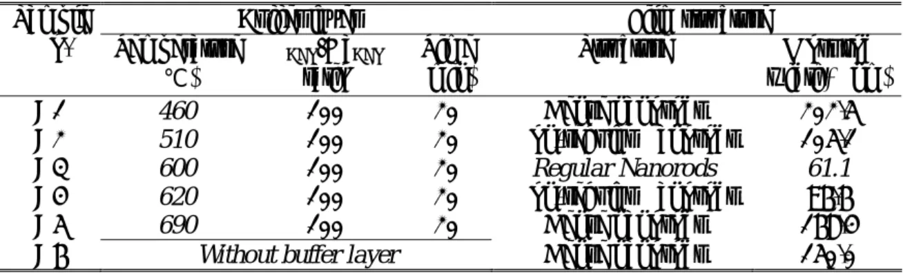
Table I Growth conditions of the GaN nanorods grown on different buffer layers. These GaN nanorods were grown at same conditions, which were temperature of 720℃, NBEP/GaBEP ratio of 40, and growth time of 5 hours.
*Most rod width: width at the peak of the rod width distribution curve.
Buffer layer Film structure
Sample
No. Temperature (℃)
NBEP/GaBEP
ratio
Time (min)
Structure Most rod
width* (nm) A1 460 100 20 Dense nanorods 202.5 A2 510 100 20 Non-regular Nanorods 105.1 A3 600 100 20 Regular Nanorods 61.1 A4 620 100 20 Non-regular Nanorods 96.6 A5 690 100 20 Dense nanorods 168.4
A6 Without buffer layer Dense nanorods 150.0
Table II Growth conditions of the GaN nanostructures grown on the sample A3 buffer structure.
Sample No.
NBEP/GaBEP
ratio Time (hr) Temperature (℃) Film structure B1 10 5 720 Only matrix B2 30 5 720 Nanorods + matrix
B3 50 5 720 Nanorods + broken matrix
Figure captions
Fig. 1
FESEM images of the GaN nanorods grown at different GaN buffer temperatures. These buffer temperatures are (a) 460 ℃ (sample A1), (b) 510 ℃ (sample A2), (c) 600 ℃ (sample A3), (d) 620 ℃ (sample A4), and (e) 690 ℃ (sample A5). (f) Sample A6 was directly grown on the Si(111) substrate. There are two kinds of nanorod structures. One is the dense nanorod structure (samples A1, A5, and A6), and the other is the isolated nanorod structure accompanied with surrounding matrix (samples A2, A3, and A4). Only buffer structure grown at temperature of 600 ℃ suits isolated nanorod growth with regular shape and size.
Fig. 2
(a) Distribution of the GaN nanorod width with different buffer layer temperatures. The nanorods grown on the buffer layer at a temperature of 600 ℃(sample A3) shows the smallest lateral width and the narrowest width dispersion. (b) Dependence of the GaN nanorod height, width, and FWHM with different buffer layer
temperatures. These nanorods show almost the same height independent on the structure, but width and FWHM of the nanorod distribution show strong correlation with the buffer structure.
Fig. 3
Three major morphologies of the GaN buffer layer grown on the Si(111) substrates: (a) granular structure grown at low temperature of 460 ℃ (buffer A1), (b) broken film grown at medium temperature of 600 ℃ (buffer A3), and (c) isolated islands grown at high temperature of 690 ℃(buffer A5).
Fig. 4
FESEM images of the GaN nanorod grown on the buffer A3 (shown in Fig. 2(b)) after 30 minutes and 3 hours growth. After 30-minutes growth: (a) surface image shows that nanorods attach the sidewall of craters, and (b) nanorods in trenches were still below the surrounding matrix. After 3-hours growth: (c) surface image shows a nanorod grown in the center of a crater, and (d) the nanorod in the trench was protruding above the matrix. The inset of Fig. 4(d) shows the root of the nanorod
grown in a large opening.
Fig. 5
Dependence of nanorod height, matrix thickness, and rod density with different growth time. Density of pad grown in large openings at zero-minute growth, that is, buffer layer, is comparable to the maximum density of the nanorods. This supports that the pad serves as a crystal seed to assist the nanorod growth.
Fig. 6
FESEM images of the GaN nanostructures grown at different NBEP/GaBEP ratios which
are (a) 10 (sample B1), (b) 30 (sample B2), (c) 50 (sample B3), and (d) 70 (sample B4). Surface morphologies of the surrounding matrixes vary from compact film to nanocomb structure as increasing NBEP/GaBEP ratio from 10 to 70. This result reflects
that the morphology of the surrounding film is dominated by the surface diffusion length of the Ga adatoms.
Growth diagrams of GaN nanorod and surrounding matrix. (a) Ga adatoms accumulate on crystal seeds in large openings to form Ga cluster via nanocapillar condensation mechanism. Because the diffusion length of the Ga adatoms is related to the NBEP/GaBEP ratio, the GaN morphology can be determined via competition
between GR and GM-L. (b) GM-L > GR, no nanorod can protrude above the matrix. (c)
GM-L ≤ GR, some nanorods can protrude above the matrix. (d) GM-L << GR ≅ GM-V,
(c)
(a)
(e)
(b)
(f)
(d)
[Fig. 1]
[Fig 2]
(a)
(b)
0 100 200 300 400 Buffer = 460 oC Peak = 202.5 nm FWHM = 64.5 nmN
a
norod N
u
m
b
er (arb. units)
Nanorod Width (nm)
Buffer = 510 oC Peak = 105.1 nm FWHM = 61.8 nm Buffer = 600 oC Peak = 61.1 nm FWHM = 24.2 nm Buffer = 620 oC Peak = 96.6 nm FWHM = 39.9 nm Buffer = 690 oC Peak = 168.4 nm FWHM = 60.7 nm Without Buffer Peak = 150.0 nm FWHM = 55.1 nm450
500
550
600
650
700
750
10
610
710
810
90
50
100
150
200
250
300
Nanorod Density (cm
-2)
Buffer Temperature (
oC)
Density
No buffer
FWHM
Peak
Peak and FWHM (nm)
(b)
(a)
(c)
(a)
(c) (d)
(b)
[Fig. 5]
0
100
200
300
800 1200
0
500
1000
1500
2000
2500
6000
8000
10
510
610
710
8Thickness and Height (nm)
Growth Time (minutes)
Average nanorod height Base film thickness Pad density
Nanorod Density (cm
-2