1
.!5V CMOS
full-swin energy efficient logic
lowpower
(EEL)
circuit suitable
VLSI
applications
9
or low-voltage and
C.C. Yeh, J.H. Lou and J.B. KuoIndexing terms: VLSI, CMOS integrated circuits, Logic circuits
A 1.5V full-swing energy efficient logic circuit is reported that is suitable for next-generation low-power VLSI applications using a low supply voltage. At 25MHz and at l S V , the power consumption of the EEL circuit is 70% of that for an ECRL circuit and 47% of that for the static circuit.
Introduction: For next-generation deep-submicron CMOS VLSI
circuits, low supply voltage and low power are the trend. Adia- batic CMOS logic circuits have been reported for their potentials for low-power VLSI applications [I ~ 41. Early adiabatic logic cir-
cuits used diodes or diode-connected devices for the purpose of precharge [2], which may have limited their advantages. Recently, an efficient charge recovery logic (ECRL) circuit using a cascode voltage switch logic concept [3, 41 has been reported to give a bet- ter performance. Since its output is not full swing, it is not appro- priate for low-voltage operation. In this Letter, a 1.5V full-swing energy efficient logic circuit suitable for low-voltage low-power VLSI is described. It will be shown that it has better noise immu- nity and a higher operation frequency.
CK CK C K 3 our EEL CKO CKI CK2 CK3 PULSEU in
n r
n
-
:.I-
_r
PUL!SED'
P U k E Z'
PULSE1 PULSE1 PULSE3 PULSE2-
e
2 2 -
L L
PULSE3 - t ) -ho id-
wart prechage recover-
and evaluation jo99/liFig. 1 1.5 V CMOS energy efficient logic (EEL) circuit
1.5 V energy efficient logic (EEL) adiabatic circuit: Fig. 1 shows the
1.5 V CMOS full-swing energy efficient logic (EEL) circuit which is derived from the ECRL circuit. As shown in the Figure, four clocks connected to the power supply are required, each having four phases. The four phases of each clock are (i) precharge and evaluate, (ii) hold, (iii) recover and (iv) wait. In the precharge and evaluate phase. the clock voltage gradually increases from OV to
V,. If the input
V,
is high and the complementary inputE
is low, the NMOS device MNl is on and the NMOS device MN2 is off. Therefore, the complementary output node is discharged to ground by MN1. Consequently MP2 turns on. As a result, the output node V,,, increases as the supply clock (CK) rises. When the supply clock (CKj enters the hold phase, both outputs (V,,,and
G )
maintain their previous values. When CK decreases froin Vdd to ground it is in the recovery phase, where charge previ- ously stored in the load capacitance at theE,,
node flows upwards to the CK supply. When CK is low, it is in the wait phase where the circuit is idle. Unlike the ECRL circuit, the EEL circuit has added the NMOS devices MNRIIMNR2 between the output node and the CK supply. When PULSE is high, MNRlIMNR2 are on. Therefore, during the wait phase, the remaining charge at the output node, which is not able to be discharged via the PMOS device, can be discharged to the CK supply via MNRlI
MNR2. Consequently, the output voltage can reach OV: full-swing of ithe output can be attained. In addition, more charge can be returned to the CK supply- a higher energy efficiency for the EEL circuit. (Note that without MNRl and MNR2 as in the ECRL
circuit, during the recovery phase. due to the threshold voltage of the PMOS device, the output voltage cannot drop to 0 V as CK falls: the output is not full-swing. As a result, the noise margin of the ECRL circuit may not be good.)
2 1 0 -1
=--
W m-
0 20 LO 60 80 time,ns mFig. 2 Transient waveforms of ECRL and E E L circuits
Frequency = 25MHz
a ECRL b EEL
Pevformance evaluation and discussion: To evaluate the perform- ance of the EEL circuit, a logic system with four EEL circuits has been designed based on a 0 . 8 ~ CMOS technology. The aspect ratio of the PMOS devices is 1010.8. The aspect ratios of the NMOS devices MNl/MN2 and MNRlIMNR2 are 5 / 0 3 and 2/03,
respectively. A capacitive load of 10% is placed at the output nodes. Fig. 2 shows the transient waveforms of a the ECRL circuit and b the EEL circuit using a 1.5V clock. Owing to the threshold voltage of the PMOS device, during the recovery phase, the output voltage V,,, of the ECRL circuit cannot follow CK to reach the ground level. Since the NMOS device MN1 is off during both the recovery and wait phases, the complementary output node is floating. Owing to clock feedthrough. the output voltage may drop to < OV. During the following precharge and evaluate phase, when the PMOS device MP1 turns on, the consumed power of MP1 is large since the voltage drop between its source and drain is large (VcK ~
G).
In the EEL circuit, during the wait phase, thecomplementary output node is no longer floating. Owing to the ~ NMOS devices MNRl and MNR2, both output nodes (V,,,,
E,,
) are pulled to the same voltage level as the CK supply,; 3 W 2
5
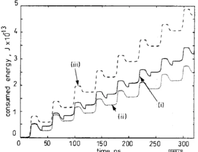
m I W c U (U v) c 8 ' 0 0 50 100 150 200 250 300 time, n sFig. 3 Consumed energy time during transient of ECRL and EEL circuits
Frequency = 25MHz Supply voltage = 1.5 V
(i) our EEL with PULSE driver (ii) our EEL without PULSE driver (iii) ECRL [9]
i.e. OV. Therefore, in the following precharge and evaluate phase, the voltage drop between the source and the drain of the PMOS device MPl is smaller than that in the ECRL circuit. Conse- quently, the consumed energy of MP1 in the EEL circuit is smaller than that in the ECRL circuit. From a power consumption point of view, a higher operation frequency can be obtained for the EEL circuit. Fig. 3 shows the consumed energy during the transients of ECRL and EEL circuits. Owing to the attachment of MNRl and MNR2, the consumed energy of the EEL circuit is smaller than that of the ECRL circuit. Including the power con- sumption of the circuit used to generate the PULSE signal [4], and within a time window of 320ns. the EEL circuit consumes 3.3 x lW3 J , which is 70% of that for the ECRL case (4.66 x lW3 J).
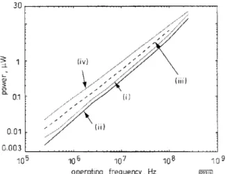
30
5 1
L3
0 a 01 0.01 0.003 i o 5 10 107 108 109 operating frequency, Hz (09914/Fig. 4 Consumed power against operating frequency of ECRL, EEL,
and static circuits at 1.5 V
Supply voltage = 1.5V (i) our EEL with PULSE driver (ii) our EEL without PULSE driver (iii) ECRL 191
(iv) static
Excluding power consumption used to generate the PULSE signal, the EEL circuit consumes 2.5 x lW3 J, which is 54% of that for the ECRL case. Fig. 4 shows the consumed power against the operating frequency of the ECRL, EEL, and the static circuits at a 1.5V clock. As shown in the Figure, when the operating frequency is lowered. among three cases, the drop in the consumed power of the EEL circuit is largest. At 250KHz, the ECRL circuit consumes 10.9nW, the static circuit consumes 21.9nW, and the EEL circuit, including/excluding the power consumption of the circuit used to generate the PULSE signal, consumes 7.315.6nW. As for the max- imum operation frequency, the EEL circuit can operate at the highest speed: 250MHz. Therefore, the EEL circuit can operate at the lowest supply voltage and highest speed; hence it is suitable for low-voltage operation.
Conclusion: In this Letter, a 1.5V full-swing energy efficient adia-
batic logic circuit has been described. At 25MHz and at ISV, the EEL circuit has an energy consumption that is 70% of that for the ECRL circuit and 47% of that for the static circuit.
Acknowledgments: This work is supported under ROC National
Science Council Contracts #86-2215-EO02-019 and #85-2622- E002-019.
0 IEE 1997
Electronics Letters Online No: 19970915
C.C. Yeh, J.H. Lou and J.B. Kuo (Department of Electrical Engineering, Room 338, National Taiwan University, Taipei, 106-1 7 Taiwan, Republic of’ China)
E-mail: [email protected]
25 April 1997
References
1 DICKINSON, A.G , and DENKER, IS.: ‘Adiabatic dynamic logic’, IEEE
J. Solid-State Circuits, 1995, 30, (3), pp. 311-315
2 LAU, K.T., and WANG, w.Y.: ‘Transmission gate-interfaced APDL design’, Electron. Lett., 1996, 32, (4), pp. 317-318
3 HELLER, L.G., and GRIFFIN, w.R.: ‘Cascode voltage switch logic: A
differential CMOS logic family’. ISSCC Dig. Tech. Papers, 1984, 4 MOON, Y . , and JEONG, D.-K.: ‘An efficient charge recovery logic
circuit’, IEEE J. Solid-state Circuits, 1996, 31, (4), pp. 514-522
pp. 16-17
2-46.5GHz quasi-static
2:l
frequency divider
IC using InAIAs/lnGaAs/lnP HEMTs
T. Otsuji, M. Yoneyama, K. Murata, Y. Imai, T. Enoki and
Y.
UmedaIndexing terms: High electron mobility transistors, Integrated circuits, Dividing circuits
The authors report a 246.5GHz quasi-static frequency divider IC using InAlAs/InGaAs/InP HEMTs. Wideband clockldata buffers and an HLO (high-speed latching operation)-type T-FF were incorporated to enhance the operating range. The IC was mounted on a dedicated IC package and operated up to 45.2 GHz.
Introduction: High-speed frequency divider ICs with a wide oper- ating range are a key component in broadband optical fibre com- munications systems. To date, 40GHz-class static frequency divider ICs have been developed using several compound semicon- ductor devices [l, 21. The record operating frequency is 40.4GHz [l], which is not acceptable for 4OGHz operation in real systems. With the advent of the dynamic operation, the maximum fre- quency can be increased to > SOGHz, but minimum frequency is sacriticed for any increases in maximum frequency beyond 25GHz [3]. Assuming a typical 40Gbitis-class optical receiver configura- tion, including up to 1.8 data demultiplexing, operation over 4OGHz with a wide frequency range of over one octave is required for the frequency divider IC.
Process technology: We used a 0.1 pn gate length InAlAslInGaAsl InP HEMT process [4]. The typical device parameters are the same as those reported in [SI. The average threshold voltage (
Kh)
is 4 . 5 V with a standard deviation of less than 40mV for a 2in wafer). The average transconductance, f T , and fm,, are 9SOmS/mm, 174GHz, and SOOGHz, respectively. The IC accommodates a standard interconnection process with double-layered Au-metal interconnection lines and air-bridges.
i
j
m
Fig. 1 Circuit block diagram o f 2 : l frequency divider IC
CBUF: clock buffer, OBUF: output buffer, DR: driver, R,: termina- tion resistor
Circuit design: The circuit block diagram of the IC is shown in
Fig. 1. To increase the maximum frequency and maintain a wide operating range, an HLO (high-speed latching operation)-type toggle flip-flop (T-FF) [6] was adopted for the core circuit. The gate width of the data latch circuit was set at one half of the data read circuit (2Opn) to increase the maximum frequency while maintaining quasi-static operation from near 1 GHz. Capacitive peaking was incorporated into the source followers of all the cir- cuit blocks, which compensates for the loss at high frequencies and results in higher speed operation. The clock buffer consists of a two-stage inductor peaking differential buffer. A capacitively- coupled resistive divider was introduced as a low-loss passive R F level shifter, instead of a source follower. The lower cutoff fre- quency of the divider was designed at less than lGHz so that a wide operating range from 1 to SOGHz was obtained. The internal