國 立 交 通 大 學
光 電 工 程 研 究 所
碩士論文
非極性氮化鎵及氧化鋅之結構及光學特性之研究
Study on structural and optical properties of
non-polar GaN and ZnO
研究生:張家銘
指導教授:郭浩中 教授
盧廷昌 教授
非極性氮化鎵及氧化鋅之結構及光學特性之研究
Study on structural and optical properties of non-polar GaN and ZnO
研究生:張家銘 Student: Chia-Ming Chang 指導教授:郭浩中 教授 Advisor: Prof. Hao-Chung Kuo
盧廷昌 教授 Prof. Tien-Chang Lu
國 立 交 通 大 學
光電工程研究所
碩 士 論 文
A Thesis
Submitted to Institute of Electro-Optical Engineering College of Electrical Engineering
National Chiao Tung University in Partial Fulfillment of the Requirements
for the Degree of Master
In
Electro-Optical Engineering
July 2008
非極性氮化鎵及氧化鋅之結構及光學特性之研究
研究生:張家銘 指導教授:郭浩中教授 盧廷昌教授國立交通大學光電工程研究所碩士班
摘要
在我的論文裡,將我的研究分成兩個部份:第一個部份是利用熱退火處理來改善a平 面的氮化鎵之材料品質,而第二部份是藉由插入a平面的氮化鎵來成長非極性的氧化 鋅。改善成長於r平面藍寶石基板上的a平面氮化鎵是在氮氣的環境上利用熱退火於已長 成的樣品上。在1000℃的a平面氮化鎵退火下,其表面的粗糙程度只有0.4奈米。X光繞 射圖更証實了晶格品質的改善。由x光的Rocking curve實驗,對[0001]方向的氮化鎵而 言 , 半 高 寬 有 隨 著 溫 度 從 850 到 1100 ℃ 逐 漸 減 少 的 現 象 。 由 穿 遂 式 電 子 顯 微 鏡 (Transmission Electron Microscope)的實驗結果指出在樣口經過1000℃的熱退火後, 螺旋差排(Treading Dislocations)沿著[0001]方向的氮化鎵從每平方公分5x10¹⁰ 減少到 每平方公分1.5x10¹⁰ ,而疊差的數量從每公分8.7x10⁵ 減少到每公分4.8x10⁵ 。室溫的光激 發螢光光譜及對應的陰極激發光影像顯示在經過熱退火處理後,比起未經過熱退火處理 的a平面氮化鎵而言,a平面氮化鎵的能帶邊緣發光強度有明顯的增加及有較大的發光區 域,其中的主要原因是非輻射復合的中心數量的減少。 在實驗的第二部份,藉由插入 a 平面的氮化鎵當緩衝層,將非極性的氧化鋅層成 長於 r 平面的藍寶石基板。由掃描式電子顯微鏡(Scanning Electron Microscope)的 觀察,隨著成長溫度的增加,氧化鋅會從似小草狀的結構轉變成薄膜的結構。X 光繞 射圖及原子力顯微鏡更証實了成長的樣品具有非極性的方向及平整的表面。由光激發 螢光譜的結果,氧化鋅薄膜有最強的近能帶邊緣的發光波長在 383 奈米並抑制了深層 能階的發光。變溫的光激發螢光譜指出,隨著溫度的增加,中性施子束縛激子和中性 受子束縛激子會漸漸的轉變成自由激子。藉由活化能的計算,當在高溫的時候,施子 束縛的激子和受子束縛的激子的活化能分別對應於激子的束縛能和能量差介於受子束 縛激子及施子束縛激子的能量,而在低溫的時候,分別對應於能量差介於施子束縛激Study on structural and optical properties of non-polar GaN and ZnO
Student : Chia-Ming Chang Advisor: Prof. Hao-Chung Kuo Prof. Tien-Chang LuInstitute of Electro-Optical Engineering
National Chiao Tung University
Abstract
In this thesis, I divide my experiments into two parts: first is the crystal quality improvement of a-plane GaN by using thermal annealing process and second is growth of non-polar ZnO film via inserting a-plane GaN. The crystal quality improvement of a-plane GaN grown on r-plane sapphire was demonstrated by applying thermal annealing on as-grown samples in nitrogen ambient. The root mean square roughness of the surface was only 0.4 nm in the 1000 °C -annealed a-plane GaN. The crystal quality improvement was confirmed by the X-ray diffraction. Full width at half maximums of X-ray rocking curve for [0001]GaN was gradually decreased when the samples were treated with annealing
temperatures from 850 to 1100℃. Transmission electron microscope resulted further indicated threading dislocations were decreased from 5× 1010 cm-2 to 1.5× 1010 cm-2 along [0001]GaN and stacking faults were decreased from 8.7× 105 cm-1 to 4.8× 105 cm-1 after the
sample was annealed at 1000 °C. Room-temperature photoluminescence (PL) and corresponding cathodoluminescence image measurements showed band edge emission intensity for a-plane GaN with annealing was enhanced and revealed larger emission area compared to the regular a-plane GaN film, which was attributed to reduction of the non-radiative recombination centers.
In the second section, non-polar ZnO film was grown on r-plane sapphire via inserting
a-plane GaN layer by using furnace. Scanning electron microscope revealed the
morphologies of ZnO were transformed from grass-like structure to thin film with increasing the growth temperature. X-ray diffraction and atomic force microscope measurements confirmed that our sample possessed non-polar crystal orientation and smooth surface. PL results exhibited the film had strongest near band edge emission of 383 nm and quenching of deep level emission. Temperature-dependent PL indicated the neutral donor-bound excitons (DoX) and accepted-bound excitons (AoX) could gradually transit to free excitons (FX) with increasing temperature. The activation energies of DoX and AoX were close to exciton binding energy and the transition variation between AoX and DoX energy for high temperature, while those were close to difference between DoX and FX and between AoX and the acceptor-donor pair for low temperature. Non-polar ZnO films have great potential for applications of novel optoelectronic.
Acknowledgement
轉眼間,兩年的時間就這麼匆匆的過去,從在成功大學懵懂無知的我來到交通大 學後,不論心態上或是處事上都有不少的成長;從實驗中,了解到現實生活中不論什麼 情況,處事都要更加的嚴慬小心,對自已我變得更加積極的面對自已的人生。 在這兩年的碩士生涯裡,我慶幸的能有三位資深的教授來指導我:王興宗教授,郭 浩中教授及盧廷昌教授。雖然碩士班只有短短兩年的學習,老師們仍是盡心盡力的指 導,即使在忙碌的階段,老師們仍願抽空和我討論,糾正我的錯誤觀念。老師們對研 究的熱忱及堅持,以及對學生的用心與指導,相信將來有一天誓必會成為世界一流的 研究室。 特別感謝博士班柯宗憲學長這兩年來的親身指導,在研究上,是一位真誠、優秀、 熱心、親切的學長,在生活上,更是一位不可或缺的良伴,除了研究上給予我相當多 的指導外,待人處事上更是給予我經驗的分享,對我無微不至的照顧,感覺就像自已 的親兄弟一樣,真是一位好的生活典範。記得在一次失敗的實驗後,當時的我心情相 當的沮喪,一整個月都無心於實驗,就在我心情最低落的時候,宗憲學長及時給予我 鼓勵,告訴我實驗的技巧與態度,讓我及時的振作並順利地度過這個難關。今天能夠 順利的畢業,真的很感謝宗憲學長的幫助,少了你,我真的不知道何時才能夠畢業。 同時也感謝其他的博士班學生,俊榮、輝閩、小朱、柏孝、士偉、明華、碩均…等, 感謝你們這兩年的照應。 謝謝這兩年來在實驗室一起努力的戰友: 柏源,駿哥,小恬恬,晁恩,子維,恕 帆,承恩,士嘉,建達,小麥。士嘉,以前和你是同學時以為你是位敦厚老實的學生, 經過了大學四年後,怎麼變得如此的嘴炮,果然人是會變的;承恩,和你聊天真是開心,很過份,那有中鋒跑到外面來投三分球的。晁恩,你做實驗的態度真是讓我折服,細 心程度和伯駿不相上下,也感謝你這兩年來的照應。柏源,同樣是湖人的球迷,一起 看球總是充滿了樂趣,明年湖人一定會拿總冠軍的。小恬恬、小麥,謝謝你們這兩年 來在實驗上的幫助,讓我可以順利完成我的實驗,也預祝小麥你也能早日的畢業;駿 哥,你對實驗的堅持是眾所皆知的,很佩服你對實驗的熱忱,總是有用不完的精力, 不過,你要改掉你的龜毛的習慣,這樣才能得到美女的親睞。和你們在一起,生活總 是充滿了笑聲,總是有說不完的八卦,和你們一起出去吃飯是我一天最開心的時刻, 一起聊天打屁,談論是非。又到時候說再見,在這裡,先預祝大家在未來都能飛黃騰 達。 碩一的學弟妹們:卓木,謝謝你在我自顧不暇的時候,幫我一起完成實驗,讓我減 輕負擔許多,希望你在未來的一年裡實驗能夠順利的完成。還有就是尚樺、小柯、政 暐、建綱、治凱、玫君、亭君、qq、生哥,預祝你們未來的一年裡,實驗能夠順利, 明年都能夠順利的畢業。 還有,要感謝的就是在交大這兩年認識得朋友,飛鴨、芯芸、宜容、查、阿欽、 芸芸、京橋、宛姍…等,有了你們讓我的碩士生活增添了許多的色彩,和你們一起出 去玩總是有一堆做不完丟臉的事情。還有猩猩,你是大家的吉祥物,有你在,周遭總 充滿歡樂,謝謝你帶給大家這麼多歡樂。 最後,感謝在交大認識的每一個人,預祝大家身體健康,事事順心。
Content
Abstract (in Chinese) ... i
Abstract (in English) ... ii
Acknowledgement ...iii
Content ... v
List of Figures ... vii
Chapter 1 Introduction and Motivation ... 1
1-1 Introduction to opto-electronic material... 1
1-2 Property of non-polar gallium nitride and zinc oxide... 4
1-3 Review of thus far achievement and motivation ... 6
1-4 Overview ... 11
Chapter 2 Theoretical Background and Experiment Apparatus ... 12
2-1 Scanning electron microscope (SEM) and Transmission electron microscope (TEM) ... 12
2-2 Atomic force microscope (AFM) ... 18
2-3 X-ray diffraction (XRD) ... 19
2-4 Photoluminescence (PL) ... 21
2-5 Furnace... 22
Chapter 3 Experiment Process, Results and Discussion ... 24
3-1 The effect of thermal annealing on non-polar a-plane GaN grown on r-plane sapphire ... 24
3-1-3 Summary...31
3-2 Growth of non-polar ZnO nanostructures and films via using a-plane GaN buffer layer ... 40
3-2-1 Samples preparation and growth...41
3-2-2 Structural and optical characterizations ...42
3-2-3 Summary...49
Chapter 4 Conclusion... 57
Chapter 5 Future work and prospect ... 59
List of Figures
Fig. 1-1-1Band bending resulted from QCSE in polar III-nitride quantum well with different
thicknesses...3
Fig. 1-2-1Schematic diagram of defects type in a-plane GaN (J. Appl. Phys. 94, 942, 2003)...5
Fig. 1-3-1 The PL spectrum of different polarization angles in m-plane GaN (a) and the comparison of PL intensity and the corresponding angle (b) (Appl. Phys. Lett. 71, 1996, 1997)...7
Fig. 1-3-2 Cross-section TEM of a-plane GaN grown on the r-plane sapphire substrate (a) and AFM image (b) (Appl. Phys. Lett. 81, 469, 2002) ...8
Fig. 1-3-3 The comparison of c-plane and a-plane AlGaN/GaN quantum well with different thickness (Appl. Phys. Lett. 84, 496, 2004) ...9
Fig. 1-3-4 AFM image of a-plane GaN without (a) and with (b) SiNx layer on the surface (Appl. Phys. Lett. 89, 041903, 2006)...9
Fig. 2-1-1 Physical mechanism of electron beam occurring on the sample...13
Fig. 2-1-2 Ray diagram for viewing the image (a) and the diffraction pattern of the sample (b). ...16
Fig. 2-2-1 The relation of the distance and interaction between the atoms...18
Fig. 2-3-1 Schematic viewing of X-ray diffractor setup ...20
Fig. 2-4-1 The schematic diagram of photoluminescence setup ...22
Fig. 3-1-1 The surface AFM image of a-plane GaN annealed at (a)850℃, (b)900℃, (c)950 ℃, (d)1000℃, (e)1050℃, and (f)1100℃. ...32
Fig. 3-1-2 The SEM images of a-plane GaN annealed at (a)850℃, (b)900℃, (c)950℃, (d)1000℃, (e)1050℃, and (f)1100℃. ...32
Fig. 3-1-3 θ-2θscan of the sample. ...33
Fig. 3-1-5 Bright field cross-section TEM images of a-plane GaN epilayer
(a)(c)without/(b)(d)with annealing at 1000℃. ...35 Fig. 3-1-6 Plane-view TEM images of a-plane GaN epilayer (a) without/ (b) with annealing
at 1000 ℃. (c)HR-TEM of Atomic layer scanning and (d)Fourier-filtered image
corresponding to the image in (c)...35 Fig. 3-1-7 The etching pits density of a-plane GaN without/with annealing at 1000℃ ...36 Fig. 3-1-8 The computations of lattice constant and mismatch under different annealing
temperature. ...36 Fig. 3-1-9 Room temperature PL spectra of the a-plane GaN annealed from 850 to 1000 ℃.37 Fig. 3-1-10 Room temperature PL spectra of the a-plane GaN annealed at different ambient
gases ...37 Fig. 3-1-11 Low temperature PL spectra of the a-plane GaN with/without annealing at 1000
℃. ...38 Fig. 3-1-12 Room temperature PL spectra of the a-plane GaN annealed at 1000℃ at
different times...38 Fig. 3-1-13 CL images show the surface emission of the a-plane GaN without/with
annealing at 1000 ℃...39 Fig. 3-2-1 Schematic drawing of growing a-plane ZnO on r-plane sapphire via inserting
a-plane GaN as buffer layer. ...50 Fig. 3-2-2 The surface SEM images of a-plane ZnO grown on r-plane sapphire via inserting
a-plane GaN as buffer layer at the temperature of (a) 700oC、(b) 800oC and (c) 900oC. (d)The cross-section SEM image indicates the thickness of the film is 3.394µm...51 Fig. 3-2-3 The surface SEM images of a-plane ZnO grown on r-plane sapphire via inserting
a-plane GaN as buffer layer at the temperature of 900oC with growth period of (a) 6 hours, (b)7 hours, (c)8hours, and (d)9 hours. ...51 Fig. 3-2-4 Schematic growth mechanism by using thermal vapor deposition on c-plane and
a-plane substrate ...52 Fig. 3-2-5 The surface AFM image of non-polar a-plane ZnO film. The RMS is 12.946nm. .52 Fig. 3-2-6 (a) the θ-2θ scan and (b) the rocking curve XRD pattern of the a-plane ZnO film.
(perpendicular) to the X-ray beam. ...53 Fig. 3-2-7 Room temperature PL spectrum of ZnO nanograss, nanosprout, and film grown
on r-plane sapphire via inserting a-plane GaN as buffer layer. ...54 Fig. 3-2-8 Temperature-dependent PL analysis of a-plane ZnO. The neutral donor-bound
exciton and acceptor-bound exciton were observed at low temperature...54 Fig. 3-2-9 The calculation of the activation energy of donor-bound exciton and
acceptor-bound exciton from the temperature-dependent PL. ...56 Fig. 3-2-10 The fitting of the peak position in donor-bound exciton and acceptor-bound
Chapter 1 Introduction and Motivation
1-1 Introduction to opto-electronic material
Nowadays, blue and UV light emitted diodes with efficiency, brightness, and longevity
that are well in excess of those required for outdoor applications are highly expectable. With
full of vital development of LEDs, LEDs have a variety of applications in the different field.
Among the applications of them are indicator lights, signs, traffic lights, background
lighting source of liquid crystal display, and lighting which requires emission in the visible
part of the spectrum…etc.. Nevertheless, the current LEDs might have difficulties in the
hard growth, low light efficiency, and large energy loss, which results in LEDs in the
application of lighting are not good enough to replace the traditional fluorescent light.
Potentially, further improvement in LEDs would be definitely required for the future life.
In recent years, the desire for blue and UV diode lasers and light emitting diodes has
prompted enormous research efforts into II–VI and III–V wideband gap semiconductors.
Among the well-known semiconductor materials employed in various technical applications,
two unique positions are held by gallium nitride (GaN) and zinc oxide (ZnO) in the wide
direct band gap semiconductor. In the material property, both GaN and ZnO have many
difference of them, the remarkable property of ZnO better than GaN is exciton binding
energy of 60 meV, which is only 30 meV for GaN. Owing to the larger exciton binding
energy, more excitons exist in the room temperature, resulting in higher luminescence than
GaN. Furthermore, ZnO can be grown at lower temperature on the cheaper substrate and
lead to low cost of growth. However, because of more intrinsic defects, the hard growth of
p-type ZnO to achieve the p-i-n junctions, and the degradation of material quality, the
current commercial blue and UV LEDs are primitively composed of GaN. However,
GaN-based LEDs still confront some problems of the luminescence, such as more defects in
the material and low electron-hole recombination of c-direction growth. Therefore, it is
worth making the further researches on the material of ZnO and GaN on purpose of
possessing well-performed LEDs and LDs.
With the concern of growth technique, the material such GaN is grown on c-plane
sapphire substrate in the field of the current commercial blue and green LEDs. The growth
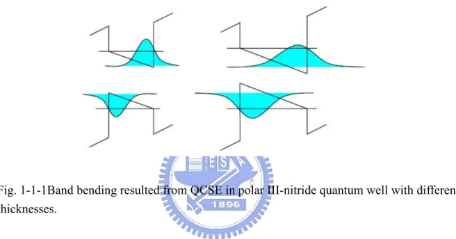
direction along c-axis could confront a problem that along the carrier flowing direction,
because of asymmetric electric charge in the atom, built-in electric field exists in the GaN
material. The causes of the built-in electric field exist two:one is different electric charges
confined stark effect (QCSE) [1][2]. The field leads to band bending and forces the carriers
to the opposite side of the quantum well. The overlapping probability of the wave function
taking place between electrons and holes would decrease, as weaken the lighting efficiency
(Fig. 1-1-1).
Fig. 1-1-1Band bending resulted from QCSE in polar III-nitride quantum well with different thicknesses.
In the limit of the direction of material growth and polarization resulted from the
hexagonal close-packed structure, the efficiency of the opto-electronic transformation is still
not good enough. New outstanding materials or other directions of growth are definitely
required to be investigated in detail. In the aspect of the non-polar plane, besides
enhancement of opto-electronic transformation, the emission light from non-polar material
is also in possession of the polarization properties, which has a great benefit in the
1-2 Property of non-polar gallium nitride and zinc oxide
The property of non-polar Gallium nitride
Gallium nitride is a III-V compound semiconductor with wide direct band gap of 3.42
eV in room temperature. Gallium Nitride is hexagonal close-packed structure with lattice
constants of a = 0.3189 nm and c = 0.5185 nm. As the growth of GaN, the primitive growth
direction is along [0001], leading to high quality and low defect in the traditional
(0001)-oriented GaN. However, on a-plane GaN, growth rate on c-axis direction is different
to m-axis direction, and the growth rate on Ga face is 4 times faster than N face on c
direction. It results in roughness surface and large dislocation. Typically, V-defect resulted
from growing on the traditional c-plane GaN would change original type, which becomes <-
defect. This defect type is aligned with [0001] and the two inclined facets are (1011) (Fig.
1-2-1). The growth direction along the [0001] conduces the parallel stripes are on the
Fig. 1-2-1Schematic diagram of defects type in a-plane GaN (J. Appl. Phys. 94, 942, 2003)
The property of zinc oxide
Zinc oxide is a II-VI compound semiconductor which unifies a couple of excellent
material properties: a large direct band gap of 3.37 eV at room temperature, high
transparency for visible light, chemical stability in terms of parasitic oxidation…etc..
Similar to GaN material, zinc oxide is hexagonal close-packed structure with lattice
constant of a = 0.3249 nm and c = 0.5209 nm. Due to its large exciton binding energy of 60
meV, ZnO is a prime candidate for ultraviolet light emitting diodes and lasers suggesting
even brighter light emission than the group-III nitrides [4]. Moreover, mixing Mg and Cd
can result in ZnO as a tunable band gap between 3.0 and 4.0 eV, which could be used for
same problem of QCSE grown on polar (0001)-oriented plane
u
Because of C6v symmetry, ZnO exhibits an optical anisotropy for transitions from three
separate p-like valence bands (Γ9v, Γ , and 7v l 7v
Γ in order of increasing transition energy
[6]) to the s-like conduction band. Excitons related to the respective valence bands are
referred to as A, B, and C excitons. The A and B transitions are allowed for light
polarization E perpendicular to the c-axis (E⊥c), where E is the electric field, and the C
transition is allowed for E parallel to the c axis (E // c). This anisotropy may provide various
applications using polarized UV lights.
7c
Γ
Intrinsic n-type defects such as oxygen vacancies (Vo) and zinc interstitials (Zni) exist
in the ZnO material. Up to 2 x 1021 cm-3 charge carriers (n-type) can lead to hardly doping
to become p-type ZnO [7]. In order to achieve the p-i-n ZnO junction, this important
problem must be overcome. Despite all reports of p-type conductivity in ZnO using various
growth methods and group-V dopant elements (N, P, As, Sb) [8], a reliable and reproducible
high quality p-type conductivity is lacking.
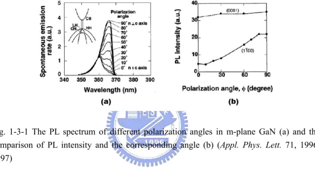
GaN on SiC by means of molecular beam epitaxy (MBE) and studied its optical properties
and polarization. As the Fig. 1-3-1 shows, at the different polarization angles, m-plane GaN
would produce discrepant photoluminescence spectra, which was due to, after valence band
splitting, different energy band have different quantities of carrier transitions.
Fig. 1-3-1 The PL spectrum of different polarization angles in m-plane GaN (a) and the comparison of PL intensity and the corresponding angle (b) (Appl. Phys. Lett. 71, 1996, 1997)
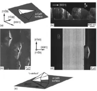
In 2002, DenBaars and Speck et al., at UCSB in America, began devoting themselves
into development of non-polar materials. They first grew a-plane GaN film on r-plane
sapphire substrate by using MOCVD, and analyzed quality by using TEM and AFM. It was
observed that treading dislocations (TDs) of a-plane GaN was up to 2.6 x 1010cm-2.
Normally, the TDs of c-plane GaN were only in the quantity of 107~108. On the other hand,
the result from AFM revealed roughness on the surface owning to a large number of
result of defects trapping radiative carrier, the quality of the film is difficulty to hold
high-efficiency radiation, even if the non-polar property theoretically has better
electron-hole recombination rate than the c-plane.
In 2003, Nakamura performed the non-polar researches, which co-worked with Speck
and DenBaars et al.. They grew about 50 µm a-plane GaN film by using HVPE. On further
step of TEM analysis, the problems mentioned above still can not be overcome. The density
of dislocation was up to 2 x 1010cm-2 (Fig. 1-3-2). DenBaars et al. compared a series of the
quantum well thickness between c-plane and a-plane GaN/AlGaN. In order to investigate
best PL intensity (Fig. 1-3-3), they find conventional c-plane GaN/AlGaN quantum well
needs only 2.8nm, but 5.2 nm for a-plane. It is due to larger dislocations result in surface
roughness, which caused non-smooth in the interface among the quantum well.
Fig. 1-3-2 Cross-section TEM of a-plane GaN grown on the r-plane sapphire substrate (a) and AFM image (b) (Appl. Phys. Lett. 81, 469, 2002)
Fig. 1-3-3 The comparison of c-plane and a-plane AlGaN/GaN quantum well with different thickness (Appl. Phys. Lett. 84, 496, 2004)
In the limit of material growth, the development of a-plane material and device is
extremely difficult. Using epitaxy lateral overgrowth (ELOG) might increase the difficulty
of processing and raise the cost. Therefore, many groups dedicated to how to improve these
non-polar materials. DenBaars et al. addressed inserting a SiNx layer as nanomask in the
growth process by using MOCVD [11]. After which growing a-plane GaN could decrease
dislocation and stacking fault down to 9 x 109 cm-2 and 3 x 105 cm-1, respectively. AFM
form Fig. 1-3-4 shows using SiNx layer can improve surface roughness.
(Appl. Phys. Lett. 89, 041903, 2006)
However, the quality of a-plane GaN grown on r-plane sapphire is usually not good
enough for high performance devices due to the lattice mismatch and critical growth
condition, which leads to a great number of threading dislocations (TDs) and stacking faults
(SFs). Previously, there are several reports using thermal rapid annealing at high
temperature to active Mg-doped GaN in a light emitting diode structure [12]. Afterward, it
was reported that the annealing process could lead to the reduction of defects and the
improvement of optical property of GaN [13] ~[15]. The annealing process is expected to be
more convenient than epitaxially lateral over-growth technique and further improve the
quality of a-plane GaN films briefly. By using a simple thermal annealing process, a smooth
surface and less defect density in annealed a-plane GaN grown on r-plane sapphire could be
beneficial to various optoelectronic device applications.
On the other hand, in recent years, ZnO are full of wide study. Although a fairly large
body of literature exists on material structure, optic, device…etc. of ZnO, so many other
niche researches of ZnO are not investigated, such as non-polar ZnO. Up to this point, there
1-4 Overview
The article is divided into three main sections. Section 1 is a description of background,
which says why GaN and ZnO are selected to perform researches. Section 2 is the briefly
introducing properties of non-polar GaN and ZnO. Section 3 is a review of the literature,
addressing both empirical and theoretical aspects of non-polar GaN and ZnO, and
motivation. This is followed by some background information on the ongoing research
within which the present study was carried on and a statement of the specific research
questions.
Chapter 2 outlines theoretical background and useful experiment apparatus to grow and
measure the sample. Chapter 3 describes experiment results and discussions, which is
separated into 2 parts. First is the effect of thermal annealing on a-plane GaN grown, and
the other is growth of non-polar ZnO nanostructures and films using a-plane GaN buffer
layer. Chapter 4 provides a conclusion of 2 part results in chapter 3. Chapter 5 is future
Chapter 2 Theoretical Background and Experiment Apparatus
2-1 Scanning electron microscope (SEM) and Transmission electron
microscope (TEM)
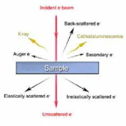
Physical mechanism of electron beam occurring on the sample can be summarized in
the Fig. 2-1-1, which is absorption, emission, reflection, transmission, and even generation
of light or X-ray emission. The secondary electrons emitted from the specimen and the
incident electrons transmitting the specimen are interesting among those generated or
inherent electrons for my measurement. Incident electrons can be focused, deflected, and
accelerated by appropriate potentials. Their energy and angular distribution can be measured
while sufficiently detected and counted. As the so-called nondestructive measurement, these
electron beam measurements exhibit good morphology characterization. However,
inasmuch as they are charged, they can cause samples charging, as may distort the
Fig. 2-1-1 Physical mechanism of electron beam occurring on the sample.
The basic structure of both SEM and TEM is illustrated above. The main spirit of the
system is the electromagnetic optical system modulating the focus, by using magnetic lens,
to form magnified image on the display. Right now, what I am going to discuss is the
principle of useful electron beam characterization techniques used in my experiment:
1. Scanning Electron Microscope
An electron microscope utilizes an electron beam to produce a magnified image of the
sample. There are three types of electron microscopes: scanning, transmission, and emission.
In the scanning and transmission electron microscope, an electron beam incident on the
sample produces image while in the field-emission microscope the specimen itself is the
source of electrons. SEM is similar to light microscope with the different manner. SEM
display, so does the TEM. The electron energy is typically 10-30 KeV for most samples, but
for insulating samples the energy can be as low as several hundred eV. The use of electrons
has two main advantages over optical microscopes: much larger magnifications are possible
since electron wavelengths are much smaller than photon wavelengths and the depth of the
field is much larger. The image in an SEM is produced by scanning the sample with a
focused electron beam and detecting the secondary or back-scattering electrons. Electrons
and photons are emitted at each beam location and subsequently detected. Secondary
electrons form the conventional SEM image, back-scattered electrons can also form an
image, X-rays are used to in the electron microprobe as to lead to the Energy Dispersive
Spectroscopy, emitted light is known as catholuminescence, and absorbed electrons are
measured as electron-beam induced current. All of these signals can be detected and
amplified synchronously via the scanning coil and then forming magnified images on the
display.
2. Transmission Electron Microscope
Transmission electron microscope is the pre-eminent method for determining
in-depth perspective of specimen characterizations.
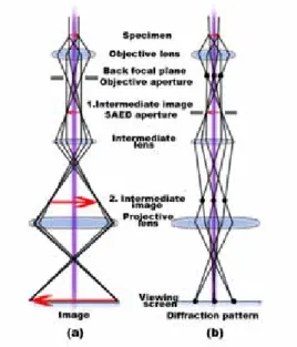
Any TEM is a complex assembly of magnetic lenses, several apertures, a sample
holder and an image recording/viewing system (Fig. 2-1-2). The objective lens forms a
diffraction pattern in the back focal plane with electrons scattered by the sample and
combines them to generate an image in the image plane (1. intermediate image). Thus ,
diffraction pattern and image are simultaneously present in the TEM. It depends on the
intermediate lens which of them appears in the plane of the second intermediate image and
magnified by the projective lens on the viewing screen. Switching from real space (image)
to reciprocal space (diffraction pattern) is easily achieved by changing the strength of the
intermediate lens. In imaging mode, and objective aperture can be inserted in the back focal
plane to select one or more beams that contribute to the final image (BF, DF, HRTEM). In
selected area electron diffraction (SAED), an aperture in the plane of the first intermediate
Fig. 2-1-2 Ray diagram for (a) viewing the image and (b) the diffraction pattern of the sample.
In the bright field (BF) mode of the TEM, an objective aperture is placed in the back
focal plane of the objective lens which allows only the direct beam to pass. In this case,
mass-thickness and diffraction contrast contribute to image formation: thick areas, areas in
which heavy atoms are enriched, and crystalline areas appear with dark contrast. In spite of
the useful information obtainable from BF images, it should be mentioned that the
interpretation of contrast is often impeded since these phenomena occur simultaneously.
In dark field (DF) images, one or more diffracted beams are allowed to pass the
objective aperture. The direct beam is blocked by the aperture. In contrast to the direct beam,
information is present in DF images, e.g., about planar defects, stacking faults or particle
size.
To obtain lattice images, a larger objective aperture has to be selected that allows many
beams including the direct beam to pass. The image is formed by the interference of the
diffracted beams with the direct beam (phase contrast). If the point resolution of the
microscope is sufficiently high and a suitable sample oriented along a zone axis, then
high-resolution TEM (HRTEM) images are obtained. In many cases, the atomic structure of
the specimen can directly be investigated by HRTEM.
The incident parallel electron wave interacts elastically while passing through the
specimen, and the resulting modulations of its phase and amplitude are present in the
electron wave leaving the specimen. The wave here, the object exit wave o(r), thus contains
the information about the object structure. The objective lens performs
1. the Fourier transform (Fourier analysis) that creates the diffraction pattern of the object in
the back focal plane and 2. the inverse Fourier transform (Fourier synthesis) that makes the
interference of the diffracted beams back to a real space image in the image plane (lattice
2-2 Atomic force microscope (AFM)
AFM shows the surface properties of the sample by means of Van Der Waals force
between the atoms. In the two atoms, one is the probe tip of the cantilever and the other is
the surface of the desired sample. The interaction between them changes with the variation
of the distance: the relation between interaction and distance is shown in Fig. 2-2-1. When
an atom is close to another, the repulsive force among electrons is larger than the attractive
force between the nucleus and electrons. Thus, the pure force of them is repulsive
interaction. On the other hand, the pure force of them is attractive interaction in the opposite
situation. In the AFM system, by means of the interaction of the tiny probe and the sample,
the fluctuation of the cantilever may be made, recoding the shift of cantilever
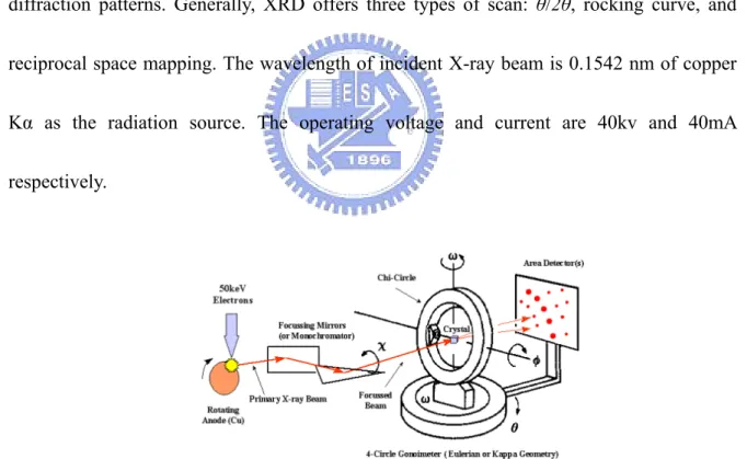
2-3 X-ray diffraction (XRD)
X-ray scattering techniques are famous of non-destructive analytical techniques which
reveal information about the crystallographic structure, chemical composition, and physical
properties of materials and thin films. These techniques are based on observing the scattered
intensity of an x-ray beam hitting a sample as a function of incident and scattered angle,
crystal orientation, and wavelength (Fig. 2-3-1).
A crystal lattice is a regular three-dimensional distribution (cubic, rhombic, etc.) of
atoms in space. Atoms among the material are arranged into its own crystal lattice. A series
of parallel planes formed in the crystal are separated from one another by a distance d,
which varies according to the nature of the material. For any crystal, planes exist in a plenty
of different orientations with its own specific d-spacing. In the diffraction, Bragg’s law
must be satisfied in any crystalline orientation, which is
2 d sin = n θ λ Eq. 2-3-1
where d is the spacing between the planes in the atomic lattice, θ is the angle between
the incident ray and the scattering planes, n is an integer determined by the order given, and
λ is the wavelength of X-ray. When a monochromatic X-ray beam with wavelength λ is
travelled by the rays reflected from planes differs by a complete number n of wavelengths.
Based on Bragg’s Law, by varying the angle θ, the value of d-spacing must be satisfied at
the corresponding angle. Plotting the angular positions and intensities of the resultant
diffracted peaks of radiation produces a pattern, which is characteristic of the sample. If a
mixture of different phases is present, the resultant diffractogram is formed by addition of
the individual patterns. According to the principle of X-ray diffraction, a wealth of structural,
physical and chemical information about the material investigated can be obtained from the
diffraction patterns. Generally, XRD offers three types of scan: θ/2θ, rocking curve, and
reciprocal space mapping. The wavelength of incident X-ray beam is 0.1542 nm of copper
Kα as the radiation source. The operating voltage and current are 40kv and 40mA
respectively.
2-4 Photoluminescence (PL)
Photoluminescence, a powerful and breakless analysis technology, can reveal the band
structure and the carrier transportation behaviors in a material. Moreover, the doping type,
band gap, composition, etc. of the bulk material or the size, path of carrier transportation,
lifetime, etc. of the nano-material will be shown in the photoluminescence spectrum.
Photoluminescence is a process in which a chemical compound absorbs photons
(electromagnetic radiation), transitioning to a higher electronic energy state, and then
radiatives photons back out, returning to a lower energy state. The period between
absorption and emission is extremely short, on the order of 10 nanoseconds. Light is
directed on a sample, where it is absorbed and imparts excess energy into the material in a
process called photo-excitation. The luminescence arising from photo-excitation is called
photoluminescence (PL). The intensity and spectral content of the photoluminescence is a
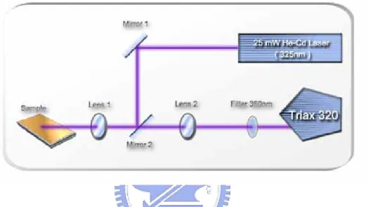
direct measurement of various important material properties. Fig. 2-4-1 shows the
schematic setup of PL system with He-Cd laser operating at 25mW at the wavelength of
325nm.
Typically, the process of the luminescence consists of three steps, which is (1)
electron-hole pairs (e-h pairs) generated by incident light recombine and create photon. In
the energy band gap, impurities and defects form a variety of energy levels, whose
corresponding energy produces radiation through radiative recombination and absorption
through non-radiative recombination.
Fig. 2-4-1 The schematic diagram of photoluminescence setup
a mechanical pump, which can exert itself to exhaust the air inside the quartz tube to the
extent of 0.01 Torr. In my experiments, two issues are performed. One is high-temperature
annealing of non-polar a-plane GaN in order to improve material quality. The other is
Chapter 3 Experiment Process, Results and Discussion
3-1 The effect of thermal annealing on non-polar a-plane GaN grown
on r-plane sapphire
The crystal quality improvement of a-plane GaN grown on r-plane sapphire was
demonstrated by applying thermal annealing on as-grown samples in nitrogen ambient. The
root mean square roughness of the 1000 °C -annealed a-plane GaN was only 0.4 nm
measured by atomic force microscopy. Transmission electron microscopy results further
indicated threading dislocations (TDs) were decreased from 5× 1010 cm-2 to 1.5× 1010 cm-2
along [0001]GaN and stacking faults (SFs) were decreased from 8.7× 105 cm-1 to 4.8× 10⁵
cm-1 after the sample was annealed at 1000 °C. Room-temperature photoluminescence
measurements showed band edge emission intensity was enhanced up to 10 folds compared
to the regular a-plane GaN film. Furthermore, corresponding cathodoluminescence (CL)
images revealed larger emission area for a-plane GaN with annealing than those without
annealing, which was attributed to reduction of the non-radiative recombination centers.
substrate at 600 °C by using metal organic chemical deposition (MOCVD). Afterward, a 2
µm-thick GaN film was grown at 1080 °C. The V/III ratio was around 900 for the growth of
bulk GaN with growth rate of 2 µm per hour. Afterwards, the as-grown samples were put
into the thermal furnace and annealed in the temperature adjusted from 850 ~ 1100 °C for 4
hours in the nitrogen and oxygen ambient.
3-1-2 Structural and optical characterizations
The surface morphology and crystal quality of the samples were analyzed by AFM,
SEM, and XRD. The TDs and SFs of the samples applied with 1000 °C annealing and
without annealing were examined by using a TEM operated at 200 KV and etching pits
density (EPD). Room and low temperature PL measurements were performed using a
continue-wave 325 nm He-Cd laser operating at an excitation level of 25 mW to investigate
the effect of annealing on luminescence enhancement of a-plane GaN. The spatially
resolved CL mappings were obtained by SEM over the samples with the same viewing
scale.
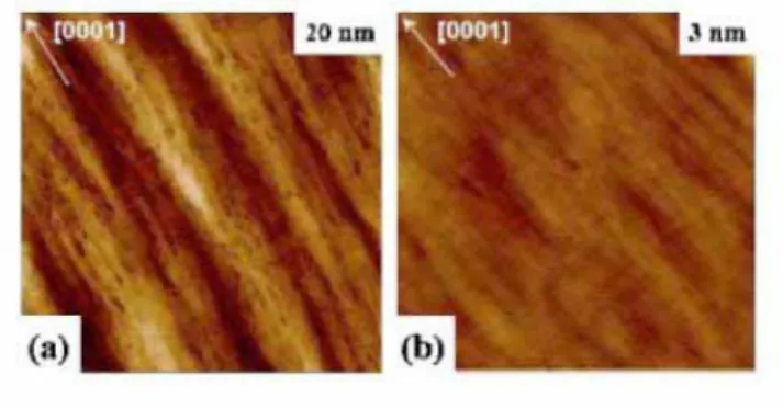
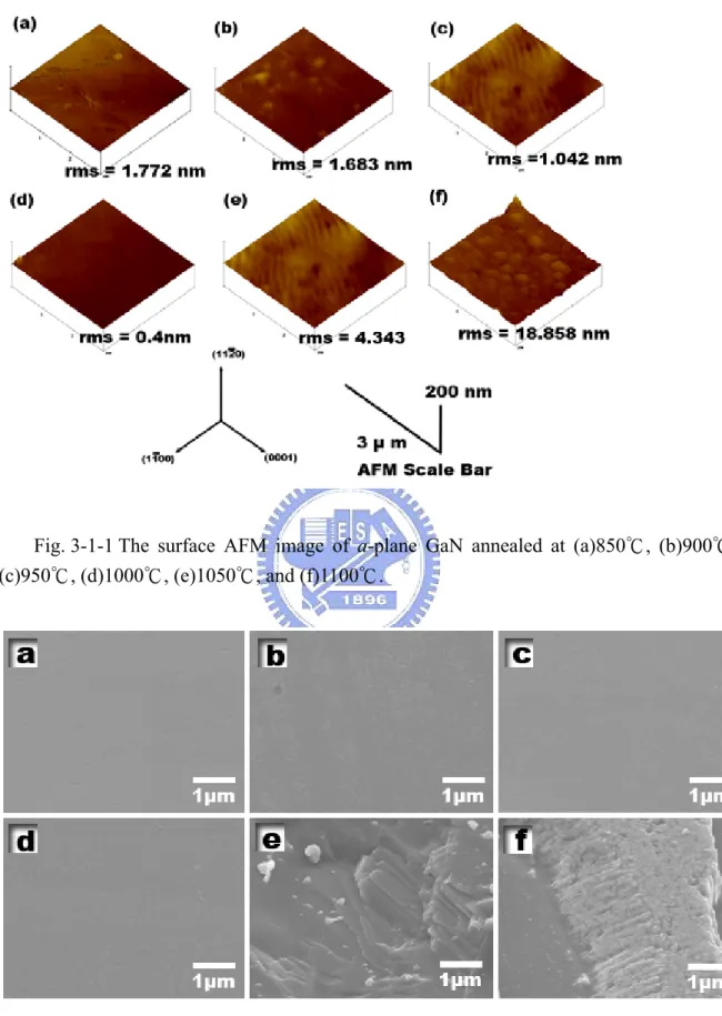
The root mean square (RMS) roughness of a-plane GaN annealed at different
temperatures was analyzed by AFM as shown in Fig. 3-1-1. The RMS of these a-plane GaN
raised from 850 to 1100 °C, which could be due to the repair of atoms near the surface. Fig.
3-1-1(d) shows the surface RMS of a-plane GaN annealed at 1000 °C is as low as 0.4 nm
compared with the RMS value of 1.1 nm for the as-grown sample without annealing. The
AFM results indicated the annealing process is benefit for surface morphology of a-plane
GaN under suitable annealing conditions. However, surface morphologies of the annealed
samples were gradually worse with increasing annealing temperature from 1000 to 1100°C,
which could be due to that the temperature of 1100 °C is close to the thermal decomposition
temperature of GaN [16].
The surface morphology was also analyzed by SEM (Fig. 3-1-2). When annealing
temperature were raised from 850℃ to1000℃, the surface of a-plane GaN was as flat as
as-grown a-plane GaN without annealing. But, it became rough at the annealing
temperature of 1050℃ and 1100℃. The collapse was clearly observed at 1100℃, which is
in consistent with AFM results.
Single crystalline a-plane GaN was confirmed by X-ray θ-2θscan, which was located
at the deflection angle of 57o (Fig. 3-1-3). The X-ray rocking curves along [0001] c and
when the samples were treated with annealing temperatures from 850 to 1100℃, whereas
the FWHM of rocking curve for [1100]GaN was gradually increased for the samples with
annealing temperature from 850 to 1050 ℃. This result implied that the crystal orientation
in the samples with annealing was getting uniform along [0001]GaN but more dispersive
along [1100]GaN [17], which could result in generation of the different strains along
[0001]GaN and [1100]GaN respectively. In addition, once the annealing temperature was
increased up to 1100 ℃, which was close to the thermal decomposition temperature, the
FWHM of rocking curve for [1100]GaN was dropped abruptly due to the stress release and
crystal relaxation along [1100]GaN from large collapsed portions of the sample.
TEM was further applied to investigate the amount of TDs and SFs in a-plane GaN
sample annealed at 1000℃ since it showed the smoothest surface which was suitable for
further device fabrication and process. The defect distributions along both c and m
directions and planar defects of our a-plane GaN films were investigated. Fig. 3-1-5 shows
the bright-field cross-sectional TEM images and Fig. 3-1-6 shows the plane-view TEM
images for our samples. Fig. 3-1-5 (a) and (b) are TEM images observed along [0001]GaN
and Fig. 3-1-5 (c) and (d) are along [1100]GaN. Fig. 3-1-5(a), and (c) in the left column are
the images for the sample without annealing and Fig. 3-1-5(b), and (d) are for the sample
calculated by Fig. 3-1-5 (a) was 5.1× 1010 cm-2. After annealing at 1000 ℃, the TD density
of the sample along [0001]GaN shows in Fig. 3-1-5(b) was reduced down to 1.5× 1010 cm-2.
On the other hand, the TD density along [1100]GaN was decreased from 6.8× 1010 cm-2 to
4.3× 1010 cm-2 calculated from Fig. 3-1-5 (c) and (d). Another way to investigate the
dislocation density was using etching pits density. Fig. 3-1-7 shows the TD density of the
sample without annealing is 1.5× 108 cm-2, which is more than the value of 0.85× 108 cm-2
with annealing.
Annealing is a useful technique that can activate disordered atoms to move to steady
positions in the crystal and further repair the crystal lattice [18], which could be main
reasons for the reduction of TDs. Except for the difference of lattice constants between
a-plane GaN and r-plane sapphire, the thermal expansion coefficients are also different in c
and m directions. We calculated the lattice constants a and c for both GaN and sapphire at
room temperature of 1000℃ by using the Eq. 3-1-1,
(
0)
∆
=
×
−
thl
C
T T
l
Eq. 3-1-1Table 3-1-1
Lattice constant (A)
Thermal expansion
coefficient (10
-6/K)
GaN Sap. GaN Sap.
c 5.185 12.991 3.17 8.5
a 3.189 4.758 5.59 7.5
According to the useful parameters in table 3-1-1, we obtained two lattice mismatches along
[0001]GaN and [1100]GaN of a-plane GaN between a-plane GaN and r-plane sapphire [17].
The calculation results indicated that the lattice mismatch at high temperature was deceased
from 1.1% to 0.6% along [0001]GaN while it was decreased from 16.1% to only 15.9% along
GaN
[1100] (Fig. 3-1-8). This could conduce to explain more reduction of TDs along
[0001]GaN than that along [1100]GaN.
On the other hand, Fig. 3-1-6 (c) shows atomic layer scanning and Fourier-filtered
image is analyzed in Fig. 3-1-6 (d). Plenty SFs were observed in Fig. 3-1-6, which were
generally observed on the c-plane sidewalls and generated from three-dimensional islands
during the initial stages of the high temperature growth. In Fig. 3-1-6, the SFs of the sample
annealed at 1000℃ decreased from 8.7× 105 cm-1 down to 4.8× 105 cm-1, which probably
attributed to the contribution of thermal annealing energy facilitating relocation of more
Fig. 3-1-9 shows the room temperature PL of the annealed samples with different
annealing temperatures. These spectra revealed the intensity of band-edge emission was
enhanced for the annealed a-plane GaN [19][20]. In our experiments, the intensity of
band-edge emission for a-plane GaN gradually increased with increasing annealing
temperature from 850 to 1000℃ and the deep level emission around 450 nm of the a-plane
GaN, which was attributed to nitrogen vacancies [35], after annealing was obviously
suppressed. The peak emission intensity of the sample with annealing at 1000℃ was
enhanced up to about 10 folds compared to the as-grown a-plane GaN film. The
enhancement of PL intensity could be attributed to fewer defects and non-radiative centers
trapping the photo-generated carriers after the sample was annealed, which is in accordance
with the TEM results. The ambient oxygen gas was also performed. Fig. 3-1-10 shows
annealing at O2 ambient is worse, which is due to defects generated from gallium oxide [22].
The enhancement of PL intensity with annealing was also confirmed in low temperature
(Fig. 3-1-11). The variation of annealing time was performed in Fig. 3-1-12. 4-hour
annealing of a-plane GaN showed the best PL intensity, which is corresponding to the least
defects. Fig. 3-1-13 shows CL emission images for samples with and without annealing at
annealing showed few and small luminescence patterns, demonstrating a worse crystal
quality of the a-plane GaN, which was consistent with room temperature PL results. As a
result, the stronger PL spectra and more uniform CL images could evidence that annealing
process on a-plane GaN could really improve the crystal quality.
3-1-3 Summary
In summary, we have demonstrated that thermal annealing process was effective for
improving the crystal quality and optical characteristics of a-plane GaN grown on r-plane
sapphire. The AFM indicated a-plane GaN annealed at 1000 ℃ has RMS of 0.4 nm. TEM
results further indicated threading dislocations was decreased from 5× 1010 cm-2 to 1.5×
1010 cm-2 along [0001]GaN and stacking faults was decreased from 8.7× 105 cm-1 to 4.8× 10⁵
cm-1 after annealing at 1000 ℃. Furthermore, room temperature PL measurements and
corresponding CL images show a-plane GaN annealed at 1000 ℃ possesses stronger band
edge emission intensity and larger emission area than that without annealing. By using a
simple thermal annealing process, a smooth surface and less defect density in annealed
a-plane GaN grown on r-plane sapphire could be beneficial to various optoelectronic device
Fig. 3-1-1 The surface AFM image of a-plane GaN annealed at (a)850℃, (b)900℃, (c)950℃, (d)1000℃, (e)1050℃, and (f)1100℃.
30 35 40 45 50 55 60 65 70 0 50000 100000 150000 200000 I ntensity (a.u.) θ- 2θ (degree) (11-20)GaN
Fig. 3-1-4 FWHMs of X-ray rocking curves for the a-plane GaN along [0001] c (Phi=0°) and [1100] m (Phi=90°) directions. The samples were annealed from 850 to 1100℃. −
Fig. 3-1-5 Bright field cross-section TEM images of a-plane GaN epilayer (a)(c)without/(b)(d)with annealing at 1000℃.
Fig. 3-1-6 Plane-view TEM images of a-plane GaN epilayer (a) without/ (b) with annealing at 1000 ℃. (c)HR-TEM of Atomic layer scanning and (d)Fourier-filtered image corresponding to the image in (c)
Fig. 3-1-7 The etching pits density of a-plane GaN without/with annealing at 1000℃
Fig. 3-1-8 (a) the computations of lattice constant and (b) lattice mismatch under different temperatures.
350 400 450 500 550 600 0 5000 10000 15000 20000 25000 Intensity (a .u.) Wavelength (nm) 850oC 900oC 950oC 1000oC 1050oC 1100oC without annealing Ambient gas : N 2
Fig. 3-1-9 Room temperature PL spectra of the a-plane GaN annealed from 850 to 1000 ℃.
350 400 450 500 550 600 0 2000 4000 6000 8000 10000 12000 14000 16000 18000 Intensity (a.u) Wavelength (nm) N2 ambient O 2 ambient without annealing
Fig. 3-1-10 Room temperature PL spectra of the a-plane GaN annealed at different ambient gases
2.8 2.9 3.0 3.1 3.2 3.3 3.4 3.5 3.6
Intensity (a.u.)
Photon Energy (eV)
with annealing without annealing @ 20 K 3.471 eV BSF PSF
Fig. 3-1-11 Low temperature PL spectra of the a-plane GaN with/without annealing at 1000℃. It implies near band edge emission at 3.471eV was enhanced after thermal annealing process. 350 400 450 500 550 600 0 5000 10000 15000 20000 25000 30000 In te n s it y ( a .u .) Wavelength (nm) 2h 4h 6h 8h Ambient gas : N 2
Fig. 3-1-13 SEM images of a-plane GaN (a) without/(b) with annealing at 1000 ℃ and corresponding CL images in (c) and (d), respectively. The emission wavelength is 362 nm.
3-2 Growth of non-polar ZnO nanostructures and films via using
a-plane GaN buffer layer
ZnO has a wurtzite structure, with the (0001) planes being Zn terminated and its
(0001) being O terminated. ZnO has a partial ionic character, which results in a partial and
opposite charge on the (0001) and (0001) planes. Thus there is a net dipole moment when
the crystal is terminated by the basal plane, and it causes the higher surface energy [23].
The (1120) and (1100) planes are non-polar and have a lower surface energy compared to
the basal plane. This results in a high growth rate along the c axis and a pillar-like
morphology grown on c-plane sapphire. For the ( ZnO films grown on r-plane
sapphire, the c axis is in the plane of the film, which results in the absence of a pillar-like
structure.
1120)
In this study, non-polar ZnO film was grown on r-plane sapphire via inserting a-plane
GaN layer by using thermal vapor deposition. Scanning electron microscope (SEM)
revealed the morphologies of ZnO were transformed from grass-like structure to films with
increasing the growth temperature. X-ray diffraction (XRD) and atomic force microscope
wavelength of 383 nm and deep level emission in the green band. Temperature-dependent
PL indicated the neutral donor-bound exciton (DoX) and accepted-bound exciton (AoX)
could gradually transit to free exciton (FX) with increasing temperature. The activation
energies of DoX and AoX were close to exciton binding energy and the transition variation
between AoX and DoX energy for high temperature, while those was close to difference
between DoX and FX and between AoX and the donor-acceptor pair (DAP) energy for low
temperature.
3-2-1 Samples preparation and growth
At first 2µm GaN film was grown on r-plane sapphire using MOCVD. The detail
growth parameters can be obtained in section 3-1-1. The sample was placed in the two-zone
furnace for growth of ZnO film. Oxygen flowing at the rate of 100 sccm was the carrier
gas.1g metal zinc was positioned upstream and the substrate was placed downstream. The
source vapor was transported by carrier gas and condensed on the substrates. The
temperatures ramped up to 900OC for sources and up to 700 OC~900 OC for substrates. The
typical reaction time was 6 hours for film and the growth pressure was around 0.1torr. The
3-2-2 Structural and optical characterizations
The morphology of the samples was investigated by SEM and AFM. Fig. 3-2-2 (a)~(c)
show the SEM images of non-polar ZnO at growth temperatures of 700 OC, 800 OC, and 900
OC, which reveal nanograss, nanosprout, and film structures, respectively. These SEM
images indicated the ZnO structures were transformed from grass-like structure to the film
with increasing the growth temperature. Fig. 3-2-3 demonstrates the best growth period of
non-polar ZnO film was 8 hours owing to flattest surface morphology. In the past, some
groups investigated the ZnO growth on the c-plane substrate by using thermal furnace [24].
However, the nano wires were often found during the experiments, which is because growth
rate of c- direction is faster than that of a- or m- direction. Fig. 3-2-4 shows, if c axis is
lying on the surface such as a-plane or m-plane substrate, the film may be achieved during
the growth owing to lower formation energy. Fig. 3-2-2 (d) shows the cross-section SEM
image revealed the ZnO film could be deposited up to 3.39µm. Furthermore, AFM is used
to analyze the surface morphology of ZnO film. The surface of the ZnO film has nanoscale
stripes running along a specific direction (Fig. 3-2-5). The direction parallel to the stripes is
determined to be [0001] direction of ZnO. It is because the growth rate along c-direction
Fig. 3-2-6 (a) shows a θ-2θ scan X-ray patterns of ZnO film which indicated that the
film have (1120) orientation, but (1101) and (1102) reflections were also observed in the
log scale, which confirmed our ZnO film was polycrystalline. Crystalline quality of the ZnO
film was addressed by X-ray rocking curve (XRC). In order to measure the in-plane mosaic,
XRC of the ZnO on-axis (1120) reflection were measured. The on-axis XRCs were
acquired with different ψangles (ψ=0o and 90o), where the ψ=0o (90o) represent that the
[0001] direction of the ZnO is parallel (perpendicular) to the X-ray beam. The FWHMs of
XRC in Fig. 3-2-6 (b) for the non-polar ZnO film were about 915 arcsec with ψ=0o and
1180 arcsec with ψ=90o. The difference in FWHMs with the ψ angles in on-axis omega
XRCs indicates that there is an anisotropic character in crystal quality in addition to the
anisotropic character in surface morphology. The smaller FWHM for the ψ=0o than that
for the ψ=90o indicates that less mosaic exists along the [0001] direction. In comparison
with recent report that c-plane ZnO thin film grown on c-plane sapphire by Zhang et al. [24],
our results revealed a-plane ZnO possessed higher crystal quality and shown a better rough
surface morphology. The prevailing cause is due to small mismatch grown on the r-plane
sapphire by inserting a-plane GaN as buffer layer. As the lattice mismatch is concerned, the
in-plane lattice period of ZnO along the [1100] direction is 3 aZnO = 0.5629 nm, while
the one of the GaN [1100]direction is 3 aGaN = 0.5524 nm. Therefore, the lattice
the [0001] direction is cZnO = 0.5207 nm, while the one of the GaN [0001] is cGaN = 0.5185
nm. Thus, the lattice misfit is as small as 0.4% which is a good approach of the lattice
constant. Both misfits along in-plane [0001] and [1100]directions are much smaller than
a-plane ZnO directly grown on the r-plane sapphire, which is 1.51% (18.31%) parallel
(perpendicular) to the axis of the [0001] direction, without inserting the a-plane GaN as
buffer layer. For this reason, ZnO film directly deposited on the underneath GaN film is
nearly lattice match growth. The different values of the misfit could be used to explain the
larger FWHM for theψ=90o might be related with the larger lattice misfit along the
[1100]ZnO//[ GaN direction. Additionally, the values measured from XRC indicates
the good crystalline quality of non-polar ZnO film, one prevailing cause of which might be
small misfit grown on the underneath GaN. Another consideration might be taken about the
thickness of the film. The FWHM from XRC of crystalline quality might decrease with
increasing thickness of the film, which results in stress release in the film. Thus, 3.39 µm
thickness of the non-polar ZnO film resulting in a relaxation of the misfit might be another
reason of good crystalline quality. 1100]
Optical property of non-polar ZnO film was measured by PL measurement with
wavelength of 383 nm in UV region was observed in the film. The UV emission is also
called near band edge emission and originated by the recombination of the free excitons at
room temperature, while the wide green band (500nm~600nm) in the visible region, known
as deep level emission, is generally explained by the recombination of the photo-generated
holes and the electrons which belong to the singly ionized oxygen vacancies [26]. This is,
the oxygen vacancies were reduced while the nanograss structure transited to the film. One
of the vital aspects of the optical characterization of non-polar ZnO film is the intensity
ratio IUV: IDL between the UV emission and the so-called green band. As the aspects of
nanograss and nanosprout structure, domination of the green level emission implies awful
material properties. For film structure, The near band edge emission dominates over the
green level emission and an IUV: IDL ratio is 7:1 at room temperature. It has been known that
if the crystal quality improves, for instance, the deposited structures show less structural
defects and low impurity contents (less oxygen vacancies, less zinc interstitials, etc.), the PL
spectra shows a sharp and strong UV emission and a suppressed and weak green emission
[27]. The reason for obtaining a good quality might be speculated on the long-time growth
of the non-polar ZnO film, which leads to the decrease of oxygen vacancies because oxygen
gas was long-time supplied oxygen atoms to repair the oxygen vacancy sites. Therefore, the
presence of a strong UV emission and weak green emission from the non-polar ZnO film
excellent optical properties.
Temperature-dependent PL spectra of non-polar ZnO film were recorded between 20
and 300 K, as shown in Fig. 3-2-8. At 20K, one of the emission lines at 3.36 eV is assigned
to the recombination of a neutral donor-bound exciton (D°X) and another emission line at
3.32 eV is identified to a neutral acceptor-bound exciton (A°X) [27]. The FWHMs of the
D°X and A°X line at 20K was measured to be 28 and 20 meV, respectively:this is a good
result because the lattice mismatch between ZnO and GaN remains small. As the
temperature increased, the donor-bound exciton and acceptor-bound exciton decreased in
energy and merged because of the thermal ionization of the excitons and the presence of
thermally activated non-radiative recombination mechanisms. For the temperature > 220K,
the PL spectra were merged into a single UV band. In order to approach its nature, the
thermal quenching of the PL integrated intensity of the UV band was studied.
The PL intensity of the donor-bound excitons and acceptor-bound excitons in the
non-polar ZnO film as a function of temperature exhibits a variation at about 80 K. One can
also see that the PL intensity of the donor-bound excitons represents a negative thermal
0 1 2 ( ) 1 exp( ) exp( ) = + − a + − a B B I I T E E A B k T k T Eq. 3-2-1
, where I0 is the peak intensity at temperature T = 0 K, A and B are parameters, Ea1 and Ea2
are the activation energies in the thermal quenching process, and kB is the Boltzmann
constant. The advantage of having a large exciton bingding energy for some device
applications is clearly seen from Eq. 3-2-1. Indeed, the PL intensity increases almost
exponentially with the activation (binding or localization) energy at a given temperature.
Fig. 3-2-9 demonstrates the integral PL intensity calculated in the UV region of energies as
a function of the inverse temperature for non-polar ZnO film. The curve in Fig. 3-2-9
represents the results of the best fit according to Eq. 3-2-1. In the case of non-polar ZnO
film, the activation energy of DoX is found to be 9 meV for T<80K and 53 meV for T>80K.
These activation energies reflect very well the properties of PL spectra in Fig. 3-2-8.
Namely, for T<80K the PL originates from the recombination of the donor-bound excitons
with the localization energy of ~9 meV﹕(D, X) → D + X, while for T > 80 K the PL
originates from the recombination of the free exciton with the binding energy of about 53
meV. The mechanism of the negative thermal quenching is the thermal activation of carriers
with energies smaller than those of the initial state of PL emission [28]. For the
observed donor-bound exciton recombination at higher energies, which can explain the
increase of the donor-bound exciton PL intensity with the temperature observed in Fig.
3-2-8. In the case of the acceptor-bound exciton, the activation energy is found to be 9.2
meV for T< 80K, while it is 39 meV for T> 80K. It is determined that for T< 80K PL can
originate from either the acceptor-bound exciton emission of recombination of the
donor-acceptor pairs, where the observed activation energy could be explained by a
transition between the acceptor-bound exciton and the donor-acceptor pair energy levels. On
the other hand, for T> 80K the acceptor-bound exciton has the activation energy of 39 meV,
which is approximately equal to the difference between donor-bound and acceptor-bound
exciton energies. It means that in this temperature region, PL is due to the recombination of
the acceptor-bound excitons and the activation energy is due to the re-localization
(donor-bound to acceptor-bound) of the exciton. The peak positions of the observed
excitonic emission lines are plotted against temperature in Fig. 3-2-10. Due to the
temperature-induced change of lattice parameters and electron-lattice interaction, the
excitonic emission energy follows the well-known Varshni equation :
2
( )
=
(0)
−
+
T
E T
E
T
α
β
Eq. 3-2-2eV/K and 900(±30)K for the two emission lines. E(0) is 3.368 eV for donor-bound exciton
emission and 3.316 eV for acceptor-bound exciton emission. The calculated temperature
dependence is demonstrated by solid curves and well fits the experimental values. The
red-shifted donor-bound and acceptor-bound excitons support their excitonic transitions.
3-2-3 Summary
In conclusion, we reported the fabrication of non-polar ZnO film on r-plane sapphire
via inserting a-plane GaN buffer layer by using thermal vapor deposition. The thickness of
non-polar ZnO film was 3.39 µm. The surface of non-polar ZnO was analyzed by AFM.
The parallel [0001) direction stripes on the ZnO surface were observed, which is due to the
growth rate along c-direction was faster than m-direction. In addition, the root mean square
roughness of non-polar a-plane ZnO is 12.9 nm. (1120) -oriented crystal phase was
confirmed by XRD θ-2θ scan and the good quality of non-polar ZnO film was obtained by
rocking curve. The FWHMs of XRC for the (1120) -oriented ZnO film were about 915
arcsec with ψ=0o and 1180 arcsec with ψ=90o, which were parallel and perpendicular to
[0001] direction. The cause is probably due to small misfit by inserting the 2 µm a-plane
GaN film as buffer layer to reduce the lattice mismatch between ZnO and r-plane sapphire.
PL measurement exhibited a sharp near band edge emission at 383 nm and an unapparent
temperature-dependent PL spectra indicated the neutral donor-bound exciton and
accept-bound exciton could gradually transit to FX with increasing temperature.
Subsequently, activation energies of D°X and A°X were found to be 9 meV and 9.2 meV
for T<80K and 53 meV and 39 meV for T>80K, repectively. Finally, such non-polar ZnO
films should have great potential for applications of novel optoelectronic devices and
nano-photonics due to this suitable fabrication process.
Fig. 3-2-1 Schematic drawing of growing non-polar ZnO on r-plane sapphire via inserting
Fig. 3-2-2 The surface SEM images of non-polar ZnO grown on r-plane sapphire via inserting a-plane GaN as buffer layer at the temperature of (a) 700oC、(b) 800oC and (c) 900oC. (d)The cross-section SEM image indicates the thickness of the film is 3.39µm.
Fig. 3-2-3 The surface SEM images of non-polar ZnO grown on r-plane sapphire via inserting a-plane GaN as buffer layer at the temperature of 900oC with growth period of (a) 6 hours, (b)7 hours, (c)8 hours, and (d)9 hours.
Fig. 3-2-4 Schematic growth mechanism by using thermal vapor deposition on (a) c-plane and (b) a-plane substrate